Model for band-edge electroluminescence from
metal–oxide–semiconductor silicon tunneling diodes
Miin-Jang Chen, Eih-Zhe Liang, Shu-Wei Chang, and Ching-Fuh Lina)Department of Electrical Engineering, and Graduate Institute of Electro-Optical Engineering, National Taiwan University, Taipei 106, Taiwan, Republic of China
共Received 6 November 2000; accepted for publication 30 April 2001兲
A detailed model is proposed to explain the electroluminescence spectrum from metal–oxide– silicon tunneling diodes. This model includes phonon-assisted processes and exciton involvement. According to this model, the main peak and the low-energy tail of the electroluminescence spectrum are attributed to the transverse optical phonon and the two-phonon assisted recombination, respectively. With very few fitting parameters, the model accurately predicts the measured electroluminescence spectra. © 2001 American Institute of Physics. 关DOI: 10.1063/1.1381000兴
I. INTRODUCTION
Electroluminescence共EL兲 from Si is an important issue for monolithic integration of optoelectronics in Si ultralarge scale integration共ULSI兲 circuits. To improve the poor lumi-nescent properties of Si, many techniques have been re-searched. They include Si/SiGe band structure engineering, nanocrystalline Si, porous silicon, Er-doped Si, and so on.1 Unfortunately, the fabrication processes for these techniques are not compatible with the standard ULSI technology. Re-cently, we have observed room-temperature EL from metal– oxide–semiconductor共MOS兲 silicon tunneling diodes.2,3The MOS tunneling diodes have the same structure as those used in ULSI circuits. In addition, the fabrication procedures are fully compatible with the present ULSI processes, showing promise for practical silicon-based optoelectronics integrated circuits. In this work, a detailed model for EL from MOS silicon tunneling diodes is presented. Physical processes in-volving phonon assistance and exciton-involved radiative re-combination are used to fit the EL spectra. The model accu-rately fits the measured EL spectra with only two fitting parameters.
Because of the indirect-band gap nature of crystalline Si, a phonon is required to provide the additional momentum for radiative recombination. At low temperature, the observed photoluminescence 共PL兲 spectra from crystalline Si are at-tributed to exciton-involved recombination with the partici-pation of phonons.4,5With PL measurement, the temperature dependence of Si band gap had also been analyzed using exciton-involved radiative transitions for the temperature range up to 1000 K.6 MacFarlance et al. measured the ab-sorption spectra of crystalline Si with high optical resolution,7showing that the exciton process appeared in the absorption spectra of crystalline Si even at room tempera-ture. These studies indicate that the optical properties of crystalline Si are strongly influenced by both excitons and phonons. Before recombination, an electron and a hole are first bounded to each other under the Coulomb attraction to
form an exciton and then recombine to emit a photon and a phonon.8Other experimental evidence also shows that a sig-nificant number of excitons are present in Si at room temperature.9–11Hangleiter deduced a strong influence of the exciton-mediated process on both the impurity and the band-to-band Auger recombination.9,10 Therefore, both excitons and phonons are taken into account in our detailed study of the EL from MOS silicon tunneling diodes.
II. DEVICE FABRICATION AND CHARACTERIZATION
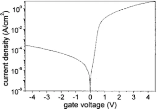
The MOS tunneling diode in this study has the ultrathin gate oxide that allows significant current to tunnel through. The ultrathin gate oxide with thickness of 30 Å was grown by rapid thermal oxidation at 900 °C on the n-type Si共100兲 substrate. The gas flows are 500 sccm nitrogen and 500 sccm oxygen at a reduced pressure. The thickness of the oxide is measured by ellipsometry and confirmed by high-frequency capacitance–voltage measurements. Transparent indium– tin–oxide共ITO兲 was deposited as the gate electrode by sput-tering with the sample held at 150 °C. The electrode with area 1.8⫻10⫺2cm2 was defined by photolithography. The thickness of the Si substrate is about 500m. Aluminum was deposited on the backside as another electrode of the MOS diode. A typical current–voltage (I – V) curve is shown in Fig. 1. At the voltages 4 and ⫺4 V, the magnitudes of the tunneling current density are 4.3 and 2⫻10⫺4A/cm2, re-spectively, showing quite fair rectification characteristics. The emission spectra correspond to the Si band gap energy pretty well. The spectra could be explained by the following theoretical model.
III. THEORETICAL MODEL
Based on the analysis of absorption spectra with the in-volvement of excitons,12the electron and the hole must meet at the same position before the phonon-assisted radiative re-combination occurs. The probability of finding an electron and a hole at the same space point can be obtained by solv-ing the hydrogen-like Schrodsolv-inger equation of the electron– hole pair, as given in the following:13
a兲Author to whom correspondence should be addressed; electronic mail:
789
兩n共r⫽0兲兩2⫽
1
aB3n3, 共1a兲
兩共r⫽0兲兩2⫽z exp共z兲
sinh共z兲 , 共1b兲
where aB is the exciton Bohr radius; n is the quantum
num-ber of the discrete exciton state; z⫽
冑
EB/(ប⫺Eg); Eg isthe band gap energy of Si; and EB is the exciton binding
energy. Equations共1a兲 and 共1b兲 specify the probability of the electron and the hole at a relative separation r⫽0 for the discrete and the continuum exciton states, respectively. The energies of the discrete and the continuum excitons are12,13
En⫽Eg⫺ EB n2⫹ ប2K2 2 M , 共2a兲 Econt.⫽Eg⫹ប 3k2 2 ⫹ ប2K2 2 M , 共2b兲
where K is the center-of-mass wave vector and k is the rela-tive wave vector of exciton; and M andare the total mass and the reduced mass of the electron–hole pair, respectively. The energy Enis quantized for the discrete states. The wave
vectors K and k are related to the wave vectors keand kh of
the electron and the hole composing the exciton by the fol-lowing formula:13
K⫽ke⫹kh, 共3a兲
k⫽mh
*ke⫺mekh
me*⫹mh* , 共3b兲
where me* and mh* are the effective masses of the electron
and the hole, respectively.
In the derivation of the emission spectrum due to the discrete exciton states, the expression should sum over the contributions from all the quantized exciton states. The wave vectors of the exciton and the phonon participating in the radiative recombination also need to be integrated to de-scribe the total spectral distribution. However, the relation of the wave vectors between the electron, the hole, and the pho-non must satisfy the requirement of momentum conserva-tion. Because the exciton consists of two Fermions, the elec-tron and the hole, such a system of two spin-1/2 particles has one singlet spin-0 state and three triplet spin-1 states.14Only the singlet spin state is taken into account for luminescence
due to the requirement of the symmetric wave function in the spatial coordinate 共兩n(r⫽0)兩2⫽0 and 兩(r⫽0)兩2⫽0兲.
Also, the spectral distribution of radiative transition is broadened as a result of the scattering of exciton by impuri-ties, electrons, holes or phonons, etc. The Lorentzian line-width broadening function is used to account for the scatter-ing effect.15 L共E21⫺ប兲⫽ 1 ប/s 共ប/s兲2⫹共E21⫺ប兲2 , 共4兲
whereSis the exciton relaxation time. In addition, because
the total spin of the exciton is an integer, the excitons follow the Bose–Einstein statistics.13Therefore, the emission spec-trum from the discrete exciton states is given by
s共ប兲⬃
兺
n 1 共2兲3冕 冕
K q d3Kd3q•兩n共r⫽0兲兩2L冉
Eg⫺ EB n2 ⫹ប 2K2 2 M ⫺Ep⫺ប冊
•␦共q⫺ke⫺kh兲 • 1 exp冉
Eg⫺ EB n2⫹ ប2K2 2 M ⫺Fx kBT冊
⫺1 , 共5兲where Epis the energy of the phonon used to compensate for the momentum mismatch between the electron and the hole in Si, Fxis the quasichemical potential of the exciton, kB is
the Boltzmann constant, and T is the lattice temperature. The factor (2)3 is the volume of each quantum state in the reciprocal space. The delta function in the integral represents the conservation of momentum for the radiative recombina-tion. Because the phonon used to compensate for the mis-match of momentum lies near the Brillouin zone edge, it is a good approximation to assume that the phonon energy Ep is
independent of the wave vector q. The quasichemical poten-tial Fx in the Bose–Einstein distribution function is
deter-mined by the total number of excitons. Assuming that the quasichemical potential Fxof excitons is below the band gap
energy Eg over many kBT, the Bose–Einstein function in
expression共5兲 is reduced to the Boltzmann distribution 1 exp
冉
Eg⫺EB n2⫹ ប2K2 2 M ⫺Fx kBT冊
⫺1 ⬇exp冉
⫺ Eg⫺ EB n2⫹ ប2K2 2 M ⫺Fx kBT冊
.The factor Fxcan then be taken out of the integral in
expres-sion共5兲, so the spectral shape is not influenced by the exact position of the quasichemical potential Fx.
Similarly, the luminescence from the ionization con-tinuum exciton states is expressed as
S共ប兲⬃ 1 共2兲3 1 共2兲3
冕 冕 冕
k q d3k d3K d3q•兩共r⫽0兲兩2 ⫻L冉
Eg⫹ ប2k2 2 ⫹ ប2K2 2 M ⫺Ep⫺ប冊
•␦共q⫺ke⫺kh兲 • 1 exp冉
Eg⫹ប 2k2 2 ⫹ ប2K2 2 M ⫺Fx kBT冊
⫺1 . 共6兲Formula 共6兲 should integrate over the variable k since the energy of the continuum exciton states is not quantized.
Be-cause we integrate over two wave vectors k and K for the continuum exciton states, the expression is divided by two unit volume (2)3. Similar to the discussion for the discrete exciton states, the Lorentzian linewidth broadening function, the requirement for momentum conservation, and the Bose– Einstein statistics obeyed by excitons are used in expression 共6兲. Only the singlet spin state is considered because of the nonzero overlap of electron and hole wave functions. The Boltzmann distribution is also applied to simplify the Bose– Einstein statistics.
From Eqs.共5兲 and 共6兲, we obtain the total emission spec-trum from both the discrete and the continuum exciton states
S共ប兲⬃
兺
n 1 共2兲3冕 冕
K q d3K d3q•兩n共r⫽0兲兩2L冉
Eg⫺ EB n2⫹ ប2K2 2 M ⫺Ep⫺ប冊
•␦共q⫺ke⫺kh兲 • 1 exp冉
Eg⫺ EB n2⫹ ប2K2 2 M ⫺Fx kBT冊
⫺1 ⫹共21兲3 1 共2兲3冕
k冕
K冕
q d3kd3Kd3q•兩共r⫽0兲兩2L冉
Eg⫹ ប2k2 2 ⫹ ប2K2 2 M ⫺Ep ⫺ប冊
•␦共q⫺ke⫺kh兲• 1 exp冉
Eg⫹ ប2k2 2 ⫹ ប2K2 2 M ⫺Fx kBT冊
⫺1 . 共7兲The temperature dependence of the band gap energy Eg can be found in Ref. 6. The widely accepted value of the exciton binding energy EB⫽14.7 meV8 is used for the calculation. The emission of transverse optical 共TO兲 phonon with Ep ⫽57.8 meV is known as the dominant mechanism for mo-mentum conservation in radiative recombination.4 – 6
Although the analysis of PL spectra of crystalline Si in Ref. 6 is also based on the concept of exciton-involved ra-diative transitions, the mathematical formula there and ex-pression 共7兲 are different. In Ref. 6, there are five fitting parameters. In comparison, our expression 共7兲 needs only two fitting parameters: T and s. The lattice temperature T
influences the linewidth through the Boltzmann distribution and the peak wavelength as a result of the temperature-dependent band gap energy Eg. The exciton relaxation time
saffects the spectral width. A major difference between our
model and the analysis in Ref. 6 is the relative magnitude of luminescence from the discrete and the continuum exciton states. Instead of treating the ratio of the contributions from discrete/continuum excitons as a free fitting parameter,6 we derive this ratio from the rigorous density-of-state and statis-tics functions.
IV. RESULTS AND DISCUSSION
Figure 1 shows typical I – V characteristics of the ITO/SiO2/n-Si tunneling diodes. When the positive gate
voltage is applied, the diode operates in the accumulation region. The positive gate voltage will inject holes from ITO to Si and attract electrons at the Si/SiO2interface to form an accumulation layer. The tunneling holes and the localized electrons in the accumulation layer form excitons, and re-combine afterward to generate radiative emission, as sche-matically shown in Fig. 2.
Figure 3 shows the calculated TO phonon-assisted emis-sion spectra from the discrete exciton and the continuum exciton states at 300 K according to expressions共5兲 and 共6兲, respectively. The discrete exciton states have stronger emis-sion than the continuum exciton states because the discrete states have more correlation between the electron and the
FIG. 2. Schematic band diagram of the ITO/SiO2/n-Si tunneling diode
hole. This indicates that the Coulomb attraction enhances the probability of finding an electron and a hole at the same position, hence improving the radiative recombination.
With significant current tunneling through the thin oxide, the luminescence could be observed through an infrared-viewer even with a low injection current density⬍1 A/cm2. The diode was operated at room temperature under cw op-eration without cooling. The EL spectra of the ITO/SiO2/n-Si tunneling diode are shown in Fig. 4. The diode had been operated at 3 and 3.5 V with injection current 88 and 133 mA, respectively. These spectra were measured using an InGaAs detector placed at the exit of a monochro-mator. The dash lines are calculated spectra using Eq. 共7兲. Temperatures at 300 and 310 K corresponding to the current at 88 and 133 mA are used for the two fitted spectra, respec-tively. Alsos⫽60 fs is used for the calculation. It is in good
agreement with the intraband carrier scattering time.16With only two fitting parameters, the theoretical prediction is pretty good.
The low-energy tail in Fig. 4 is due to the two-phonon process in the radiative recombination. The PL spectrum of the MOS tunneling diode at low temperature is shown in Fig. 5. There are three major peaks corresponding to two-phonon, TO, and transverse acoustic 共TA兲 phonon-assisted recombi-nation processes, respectively.4The two-phonon process in-volves the emission of a momentum-conserving TO phonon and a zone center (O⌫) phonon.4When the temperature in-creases to room temperature, the signal of the two-phonon
process gradually mixes with the main TO peak and forms the low-energy tail similar to Fig. 4. Decomposition of the calculated EL line shape in Fig. 4 to the main TO peak and the two-phonon signal is demonstrated in Fig. 6. The emis-sion spectrum of the two-phonon process is obtained using Eq. 共7兲 with Ep⫽57.8⫹64.5 meV (TO⫹O⌫).
4
The ratio of the magnitude between the two-phonon and the TO peaks is 0.07, which is the same as the relative magnitude of the two signals in the PL spectrum at 26 K.4The excellent match of the theoretical spectrum to the measured data in Fig. 4 indi-cates that the exciton-involved radiative recombination and the participation of optical phonons take place in the room-temperature EL from MOS silicon tunneling diodes.
We also fit the low-temperature PL spectrum in Fig. 5 using expression 共7兲 to further confirm the validity of our theoretical model. The phonon energies Ep⫽57.8
⫹64.5 meV 共TO⫹O⌫), 57.8 meV共TO兲, and 18.3 meV 共TA兲, are used in Eq. 共7兲 to fit the three peaks, respectively. With the parameters T⫽65 K and s⫽220 fs, the linewidth and
the position of peak wavelength are well predicted by the model. In the PL measurement, the cold finger is cooled at 12 K. The temperature increase for the model could be ex-plained by the local heating of the sample under argon laser excitation intensity 35 W/cm2. Figure 5 also shows a good match between the theoretical model and the measured PL spectrum.
Possible reasons for the occurrence of EL from the MOS silicon tunneling diodes at room temperature are discussed as follows. The roughness of the Si/SiO2interface is shown to be important for EL from the MOS tunneling diodes.3,17 It has been proposed that the effect of quantum confinement FIG. 3. Theoretically calculated TO phonon-assisted luminescence spectra
from the discrete exciton states and the continuum exciton states at 300 K, respectively.
FIG. 4. Room-temperature EL spectra from ITO/SiO2/n-Si tunneling diode
and the theoretical fittings.
FIG. 5. Low-temperature PL spectrum from the MOS tunneling diode.
FIG. 6. Calculated emission spectra of the TO phonon and the two-phonon assisted recombination.
will assist the formation of excitons and enhance the prob-ability of radiative transitions.18,19 The dimension of the quantum confinement system is typically on the order of the Bohr radius of exciton. The roughness at the Si/SiO2 bound-ary could provide the weak two-dimensional quantum con-finement along the plane of the interface. The carriers are also confined in the accumulation layer due to the applied electrical field. The interface roughness and the electrical field then result in a three-dimensional quantum confinement for excitons. Therefore, in addition to the extra momentum contributed from the carrier scattering due to the interface roughness,3,17 the roughness could help in the formation of exciton for enhanced luminescence.
V. CONCLUSION
In summary, EL from MOS silicon tunneling diodes is analyzed using the model of phonon-assisted and exciton-involved radiative recombination. There is an excellent fit between the model and the measured EL spectra with only two fitting parameters. The dominant peak and the low-energy tail of the EL spectrum are attributed to the TO pho-non and the two-phopho-non assisted recombination, respec-tively. The model demonstrates that the participation of optical phonons and the involvement of excitons could occur in the room-temperature EL from the MOS silicon tunneling diodes.
ACKNOWLEDGMENTS
This work is supported in part by the National Science Council, Taipei, Taiwan, R. O. C. under Contract Nos. NSC89-2215-E-002-016 and NSC89-2112-M-002-034.
1D. J. Lockwood, Light Emission in Silicon: From Physics to Devices 共Academic, New York, 1998兲.
2
C. F. Lin, C. W. Liu, M. J. Chen, M. H. Lee, and I. C. Lin, J. Appl. Phys.
97, 8793共2000兲.
3C. W. Liu, M. H. Lee, M. J. Chen, I. C. Lin, and C. F. Lin, Appl. Phys.
Lett. 76, 1516共2000兲.
4
P. J. Dean, J. R. Haynes, and W. F. Flood, Phys. Rev. 161, 711共1967兲.
5J. R. Haynes, M. Lax, and W. F. Flood, J. Phys. Chem. Solids 8, 392 共1959兲.
6V. Alex, S. Finkbeiner, and J. Weber, J. Appl. Phys. 79, 6943共1996兲. 7
G. G. Macfarlane, T. P. Mclean, J. E. Quarrington, and V. Roberts, Phys. Rev. 111, 1245共1958兲.
8R. A. Smith, Semiconductor, 2nd ed. 共Cambridge University Press,
New York, 1978兲.
9A. Hangleiter, Phys. Rev. Lett. 55, 2976共1985兲. 10
A. Hangleiter, Phys. Rev. B 35, 9149共1987兲.
11D. E. Kane and R. M. Swanson, J. Appl. Phys. 73, 1193共1993兲. 12T. P. McLean, in Progress in Semiconductor, edited by A. F. Gibson
共Heywood, London, 1960兲, Vol. 5.
13H. Barry Bebb and E. W. Williams, in Semiconductor and Semimetals,
edited by R. K. Willardson and A. C. Beer共Academic, New York, 1972兲, Vol. 8.
14E. Merzbacher, Quantum Mechanics, 3rd ed.共Wiley, New York, 1998兲. 15A. Yariv, Quantum Electronics, 3rd ed.共Wiley, New York, 1989兲. 16
K. Hess, Advanced Theory of Semiconductor Devices 共Prentice Hall, Englewood Cliffs, NJ, 1988兲.
17C. W. Liu, M. H. Lee, M.-J. Chen, C.-F. Lin, and M. Y. Chern, IEEE
Electron Device Lett. 21, 601共2000兲.
18A. L. Efros and Al. L. Efros, Semiconductors 16, 1209共1982兲. 19