Carbon attachment on the aluminum nitride gate dielectric in the pentacene-based
organic thin-film transistors
Hsiao-Wen Zan, Cheng-Wei Chou, Chung-Hwa Wang, Ho-Tsung Song, Jenn-Chang Hwang, and Po-Tsung Lee
Citation: Journal of Applied Physics 105, 063718 (2009); doi: 10.1063/1.3093686
View online: http://dx.doi.org/10.1063/1.3093686
View Table of Contents: http://scitation.aip.org/content/aip/journal/jap/105/6?ver=pdfcov Published by the AIP Publishing
Articles you may be interested in
Photochemical control of the carrier mobility in pentacene-based organic thin-film transistors Appl. Phys. Lett. 96, 213303 (2010); 10.1063/1.3432672
Low-voltage high-performance organic thin film transistors with a thermally annealed polystyrene/hafnium oxide dielectric
Appl. Phys. Lett. 95, 243302 (2009); 10.1063/1.3268455
Gate bias stress effects due to polymer gate dielectrics in organic thin-film transistors J. Appl. Phys. 103, 044506 (2008); 10.1063/1.2884535
Effect of surface free energy in gate dielectric in pentacene thin-film transistors Appl. Phys. Lett. 89, 112126 (2006); 10.1063/1.2354426
Organic thin-film transistors with nanocomposite dielectric gate insulator Appl. Phys. Lett. 85, 3295 (2004); 10.1063/1.1806283
Carbon attachment on the aluminum nitride gate dielectric
in the pentacene-based organic thin-film transistors
Hsiao-Wen Zan,1,2,a兲 Cheng-Wei Chou,1 Chung-Hwa Wang,3 Ho-Tsung Song,2 Jenn-Chang Hwang,3and Po-Tsung Lee1,2
1
Department of Photonics and Institute of Electro-Optical Engineering, National Chiao Tung University, HsinChu 300, Taiwan
2Department of Photonics and Display Institute, National Chiao Tung University, HsinChu 300, Taiwan 3Department of Materials Science and Engineering, National Tsing Hua University, HsinChu 300, Taiwan
共Received 28 October 2008; accepted 28 January 2009; published online 27 March 2009兲 This study presents carbon attachment on an aluminum nitride共AlN兲 gate dielectric to improve the device performance of pentacene-based organic thin-film transistors 共OTFTs兲. This approach produces high OTFT performance on an aged AlN surface. A high mobility of 0.67 cm2/V s was achieved on an AlN surface aged for 14 days, compared to a mobility of 0.05 cm2/V s on an as-deposited AlN surface. This improvement in device performance is correlated with carbon attachment on the AlN surface, which lowers surface energy. The lowered surface energy made the surface less polar, as measured by a contact angle instrument. The chemical composition of the aged AlN surface was analyzed using x-ray photoelectron spectroscopy before pentacene deposition. Enhanced C = C bonding at 284.5 eV was observed on the aged AlN surface. These enhanced C = C bonds favored the growth of large pentacene islands in the initial growth stage, which may improve OTFT device performance. © 2009 American Institute of Physics.
关DOI:10.1063/1.3093686兴
I. INTRODUCTION
Due to their low-temperature processing and low-cost manufacturing, organic thin-film transistors共OTFTs兲 are cur-rently the focus of considerable research for applications re-quiring displays and flexible electronics.1–3 However, the high operating voltage of organic transistors remains a limi-tation. The operating voltage can be lowered by enhancing capacitance with a thin gate dielectric4 or a high-dielectric-constant共high-k兲 gate dielectric.5Aluminum nitride共AlN兲 is a high-k material with a low operating-voltage gate dielectric used in pentacene-based OTFTs.3 AlN films have high chemical and physical stability, as well as high dielectric permittivity.6 For pentacene-based OTFT applications, the AlN dielectric can be fabricated at a low temperature 共⬃150 °C兲 using a radio-frequency 共rf兲 sputtering system. The AlN dielectric has a similar surface energy to pentacene.3
This article presents a discovery of attaching carbon to the AlN gate dielectric surface that greatly improves the per-formance of OTFT devices. Carbon is attached on the AlN surface in a dry box before pentacene deposition. Carbon attachment is a common phenomenon that has been studied in indium tin oxide and organic light-emitting devices.7,8 Low surface energy and high water contact angle after car-bon attachment on the surface were reported.9In pentacene-based OTFTs, surface energy is a key issue affecting penta-cene growth. Previous studies show that pentapenta-cene growth on surfaces with a low surface energy increases device
performance.10,11Carbon attachment causes variations in sur-face energy, which may become an important issue in fabri-cating high performance OTFT devices.
II. EXPERIMENTAL PROCEDURES
A. Film deposition and device fabrication procedures
Heavily doped n-type silicon共100兲 wafers with a doping concentration of 5⫻1015 cm−3were used as substrates. 1000 Å AlN film was deposited on these silicon wafers. The AlN film was deposited at a low temperature共150 °C兲 共substrate temperature兲 using a rf-sputtering system.3,12 Before AlN film deposition, the silicon wafer was cleaned with de-ionization water共DI water兲 and then acetone in an ultrasonic cleaner. The wafer was then dipped in diluted HF solution 共HF:H2O = 1 : 100兲 to remove native oxide from the silicon wafer. Finally, the wafer was immediately transferred to the rf-sputtering system. The system was set to a base pressure of less than 2⫻10−6 torr before admitting gas. Mass flow controllers monitored mixed argon and nitrogen gas at an Ar/N2ratio of 2/9. The total pressure for AlN film deposition was 2.5 mtorr. All relevant experimental details have been published elsewhere.3,12 After AlN film deposition, the samples were placed in a dry box共Ace Dragon Corporation’s Dr. Storage Series, model AD315兲 for different periods of time, allowing the AlN surface to absorb different amounts of carbon. Humidity in the dry box was set to 35% at room temperature. A rectangular piece of pentacene 共Aldrich Chemistry, not purified兲 defined by a shadow mask was then deposited on the AlN surface. The AlN/Si共100兲 substrate was heated to 70 ° C during pentacene deposition at a pressure of 3⫻10−6 torr. The pentacene film was 1000 Å thick, and the a兲Author to whom correspondence should be addressed. Electronic mail:
0021-8979/2009/105共6兲/063718/5/$25.00 105, 063718-1 © 2009 American Institute of Physics
deposition rate was 0.5 Å/s as monitored by a quartz crystal oscillator. Finally, 100 nm thick Au pads were deposited through a shadow mask to function as the source and drain contacts. The device channel width and length were defined as 1000 and 400 m.
B. Characterization
X-ray photoelectron spectroscopy共XPS兲 共model ESCA PHI1600兲 was used to analyze the surface composition and chemical bonding states of a material using a monochro-mated Mg K␣ line at 1253.6 eV. The instrument base pres-sure was 5⫻10−9 torr. The C 1s at 284.5 eV was used as a reference for all detected peak positions. To separate chemi-cal bonding states in the XPS spectra, the spectral line shape was simulated using a suitable combination of Gaussian and Lorentzian functions.
This study used contact angle measurements to deter-mine the migration of hydrophobic and hydrophilic func-tional groups. The water contact angle was sensitive to the chemical composition of the film surface.13 The contact angles in this study were obtained by the KRŰSS contact angle system for universal surface testing 共model GH-100兲. Material surface energy was then derived using three stan-dard liquid contact angles 共DI water, diiodo-methane, and ethylene glycol兲. The surface energy was calculated using Fowkes and Young’s approximation, as in Eq. 共1兲 关Eq.
共1兲兴,14,15 共1 + cos兲␥L= 2共␥S d␥ L d兲1/2+ 2共␥ S p␥ L p兲1/2 , 共1兲
whereis the measured contact angle,␥Lis the tested liquid surface energy and is the sum of its dispersion␥L
d and polar part ␥L p , and␥S d and␥S p
are the dispersion and polar compo-nents, respectively, of solid surface free energy. The contact angles of three standard liquids 共DI water, diiodo-methane, and ethylene glycol兲 were measured to obtain values of␥S d and ␥S
p
. All relevant surface energy details have been ana-lyzed elsewhere.16
III. RESULTS AND DISCUSSION A. Device characteristics
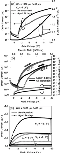
Pentacene-based OTFTs were fabricated on AlN dielec-tric surfaces that were aged in a dry box for various periods of time. Differences in aging time revealed the effect of car-bon attachment on the performance of AlN dielectric OTFTs. All electrical characteristics of OTFTs were measured using Agilent 4156 and Agilent 4284 analyzers. Figure 1共a兲 com-pares the transfer characteristics of OTFTs fabricated on an as-deposited AlN surface and on an AlN surface that was aged共with carbon attached兲 in a dry box for 14 days. TableI
lists the typical parameters of OTFTs extracted from the data in Fig. 1共a兲, including mobility, threshold voltage, Ion/Ioff current ratio, subthreshold swing, and interface state density 共NS.S.兲. The mobility and threshold voltage values are ex-tracted by the slope and intercept of the square root of drain current 共ID兲 versus gate voltage 共VG兲 curves in Fig. 1共a兲, respectively. The interface state density was extracted using Eq.共2兲, as proposed in Ref.17,
NS.S.=
冋
S log共e兲 kT/q − 1
册
Ci
q, 共2兲
where q is the electron charge, S is the subthreshold swing, T is the temperature, k is the Boltzmann constant, and Ci is the insulator capacitance per unit area.
FIG. 1. 共a兲 The transfer characteristics of OTFTs fabricated on the as-deposited AlN surface and on the AlN surface that was aged for 14 days. The square roots of IDvs VGon the respective samples plotted on the right
y-axis.共b兲 The hysteresis in the transfer characteristics of OTFTs fabricated
on the as-deposited and the 14 day aged AlN surfaces. The leakage-current densities of the Au–AlN–Au structures are plotted as a function of electric field for the as-deposited AlN and the 14 day aged AlN.共c兲 The output characteristics of OTFTs fabricated on the respective AlN surfaces.
TABLE I. Extracted parameters of OTFTs under different conditions. FE 共cm2/V s兲 VTH 共V兲 Ion/Ioff S.S. 共V/decade兲 NS.S. 共cm−2eV−1兲 As-deposited 0.05 ⫺2.2 4.5⫻103 0.64 3.8⫻1012 Aged 14 days 0.67 ⫺2.37 9.9⫻104 0.20 0.91⫻1012
063718-2 Zan et al. J. Appl. Phys. 105, 063718共2009兲
Figure1共b兲shows the hysteresis of OTFT transfer char-acteristics关Fig.1共a兲兴. OTFTs fabricated on the 14 day aged AlN surface markedly outperformed OTFTs on the as-deposited AlN surface. OTFTs fabricated on the 14 day aged AlN surface exhibited steep subthreshold characteristics 共S.S.兲, low hysteresis, high field effect mobility 共FE兲 in the saturation region, and low interface trap density共NS.S.兲. The right side of Fig.1共b兲shows the leakage-current densities of the AlN dielectrics共aged or not兲, which were measured using the Au/AlN/Au structure. The top of this figure also shows the electric field across the Au/AlN/Au structure. The leakage-current density on the 14 day aged AlN surface slightly increases. This increase in leakage-current density indicates the existence of an additional route for charge to transfer after the exposure of AlN to air. Note that the leakage-current densities in all samples aged for 14 days are below 10−7 A/cm2, which still meets OTFT requirement.
Figure 1共c兲 plots the output characteristics of OTFT samples. A higher output current occurs in OTFTs fabricated on the aged AlN surface. Figure2 compares the field effect mobilities of OTFTs fabricated on AlN surfaces aged at vari-ous times. In the field of organic electronics, mobility usually varies from device to device. The level of variation is ex-pressed by an error bar that was calculated from five differ-ent devices with the same fabrication condition. Higher field effect mobilities occur for the pentacene-based OTFTs fabri-cated on aged AlN surfaces. Mobility increases with the AlN surface aging time. OTFTs fabricated on the 14 day aged AlN surface exhibited the highest mobility at 0.67 cm2/V s. This improved carrier transport is attributed to the pentacene growth on the carbon attached AlN surface. The following sections describe and discuss this carbon attachment phe-nomenon and influence for pentacene-based OTFTs.
B. AlN film surface energy
Low dielectric surface energies can improve the carrier mobility of pentacene-based OTFTs.10,11 Research shows that hydrophobic dielectrics provide a low energy surface that matches pentacene thin films. The hydrophobic surface 共low surface energy兲 enables the pentacene molecules to align vertically in favor of carrier hopping among the
-orbitals, thus improving electrical characteristics.11
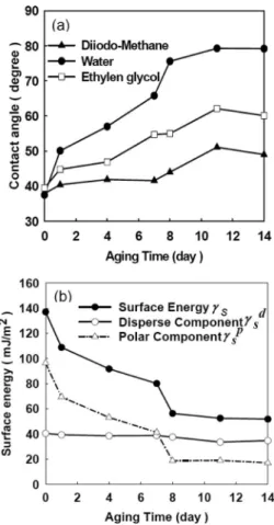
The circle symbol in Fig.3共a兲represents the water con-tact angles on the AlN surface over various aging times. The water contact angles are approximately 38.3° on the as-deposited AlN surface and 79.2° on the AlN surface aged for 14 days. The water contact angle increases with aging time. The surface energy is derived from the measured liquid con-tact angles of DI water, diiodo-methane, and ethylene glycol in Fig. 3共a兲. Figure 3共b兲 plots the surface energy and their corresponding polar and dispersive components. The surface energy and its polar component decrease as the aging time increases. This indicates that the reduction in surface energy is primarily due to the decrease in the polar component. The reduction in the surface energy’s polar component over aging time is attributed to carbon attachment based on the XPS C 1s spectra presented in Sec. III C.
C. Surface chemistry of aged AlN film
To understand the surface chemistry of carbon on an aged AlN surface, the AlN surfaces were characterized using XPS. Figures4共a兲and4共b兲show the XPS C 1s spectra from the as-deposited and 14 day aged AlN surfaces. The curve-fit data in Figs.4共a兲and4共b兲indicate that the C 1s signal con-sists of a C = C peak at 284.5 eV, a C–O peak at 286.7 eV, and an O – C = O peak at 288.5 eV.18–20 An increased C = C peak intensity appears on the aged AlN surface. The en-hanced C 1s peak at 284.5 eV corresponds to C = C bonds, suggesting the occurrence of carbon attachment on AlN sur-FIG. 2. Field effect mobility共FE兲 of OTFTs on AlN surfaces as a function
of aging time.
FIG. 3.共a兲 Water contact angles and 共b兲 the corresponding surface energies on the AlN surface as a function of aging time.
faces. The enhanced carbon attachment on the AlN surface makes the surface hydrophobic and lowers the surface en-ergy.
The carbon required for carbon attachment to occur probably comes from the atmosphere during sample transfer or from the surface of the dry box at room temperature. However, the following argument shows that carbon in the atmosphere is most likely not the possible source of contami-nation. The AlN surface energy maintains the same value if the as-deposited AlN is removed from the deposited chamber and then put into a vacuum bag for 30 days at less than 1 atm using a vacuum sealing system 共FoodSaver Co., model VAC550兲. This means that the short air exposure time before putting the AlN samples into the vacuum bag would not affect the AlN surface energy. In other words, the change in AlN surface energy is due to carbon desorption from the surface of the dry box at room temperature for a long stay time.
The signals of oxidized carbon components, C–O and O – C = O, decrease when carbon attaches to the AlN surface. This result agrees with the reduction in polar component surface energy at longer aging times in Fig.3共b兲. This reduc-tion in surface energy is thus attributed to carbon attachment that may enhance C = C bonds and reduce the relative amount of C–O and O – C = O bonds on the aged AlN surface. Carbon attachment reduces polar functional groups and surface en-ergy to match the pentacene surface enen-ergy. Similar to the
dielectric surface treated with a self-assembled monolayer 共SAM兲 before pentacene growth, the organic SAM material increases the C = C signal on the dielectric surface and en-hances the performance of pentacene-based OTFTs.16,21,22
D. Pentacene morphology
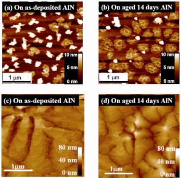
The reduction in surface energy plays an important role in affecting pentacene growth and morphology. Figures
5共a兲–5共d兲present atomic force microscope共AFM兲 images of pentacene deposited on an AlN surface. These AFM images were measured using an AFM共Dimension 3100, Digital In-strument兲 in tapping mode. Surface roughness and surface energy affect pentacene growth. Previous research shows that surface roughness has an effect on pentacene growth.23,24 The AlN surface roughness remains about the same after aging for 14 days. The surface roughnesses of all AlN surfaces remain at 0.24⫾0.02 nm. Therefore, penta-cene growth is not affected by surface roughness in this study. Figures 5共a兲and5共b兲 show the morphologies of pen-tacene islands on the as-deposited AlN surface and the 14 day aged AlN surface in the initial deposition stage. The AFM images above demonstrate that a fixed amount of pen-tacene deposited on the aged AlN surface creates larger is-lands and covers a larger area than the same amount of pen-tacene deposited on the as-depositing AlN surface. The fixed amount of pentacene was controlled using the same deposi-tion rate and deposideposi-tion time in the same run. Pentacene covers approximately 29% of the as-deposited AlN surface and 53% of the 14 day aged AlN surface. The larger island size and area coverage on the aged AlN surface are strongly correlated with a lower AlN surface energy due to carbon attachment. The C = C bonds on the aged AlN surface seem FIG. 4. XPS spectra of C 1s core levels from the共a兲 as-deposited and 共b兲 14
day aged AlN surface. The binding energy共BE兲 position and peak area of the curve-fit data are listed in the inserted table.
FIG. 5. 共Color online兲 The AFM images of pentacene on 共a兲 the as-deposited AlN and on共b兲 the 14 day aged AlN in the initial deposition stage. The AFM images of 1000 Å thick pentacene on共c兲 the as-deposited AlN surface and on 共d兲 the 14 day aged AlN surface. The surface height is expressed by the relative contrast in the AFM images on the z-axis scale.
063718-4 Zan et al. J. Appl. Phys. 105, 063718共2009兲
to enhance the larger pentacene island growth and greater area coverage. Moreover, high pentacene coverage may pro-duce the high OTFT performance reported by Kelley et al.25 Pentacene voids seem to form more easily at the island boundaries when the pentacene islands exhibit lower cover-age. The probable voids in island boundaries may limit car-rier transport and decrease carcar-rier mobility.26It was reported that voids and successive incomplete layers共islands兲 can be reduced by pentacene deposition on a low surface energy gate dielectric or a low polar energy surface.26These results are consistent with the surface energy, mobility, and hyster-esis data presented in Secs. III A and III B.
Figures5共c兲and5共d兲show AFM images of 1000 Å thick pentacene deposited on as-deposited AlN surfaces and 14 day aged AlN surfaces, respectively. Large and dendritelike grains appear in the thick pentacene film grown on both kinds of AlN surface. The pentacene grain on the as-deposited AlN surface is larger than that on the 14 day aged AlN surface. A strong correlation exists between pentacene morphology and device performance, and a larger pentacene grain size usually exhibits higher mobility. However, the re-sults of this study seem to show the opposite of this. The level of OTFT mobility reflects the carrier transport near the pentacene-AlN interface. The pentacene grain size at the ini-tial stage is more dominant, as shown in Figs.5共a兲and5共b兲 above. Pentacene islands are larger on the 14 day aged AlN surface than on the as-deposited AlN surface. The improved pentacene-based OTFT carrier transport on the aged AlN sur-face is thus attributed to larger pentacene islands near the carrier transport channel.
Moreover, the performance of OTFT devices can also be affected by various factors, including dielectric surface roughness and dielectric surface wetting properties.23 Knipp
et al. showed that the pentacene grain exhibits high electrical
characteristics when the dielectric surface chemistry became hydrophobic. Note that the 14 day aged AlN surface is also hydrophobic, which may contribute to the higher mobility of the OTFTs.
IV. CONCLUSION
This study investigates carbon attachment on the AlN gate dielectric in pentacene-based OTFTs and establishes the relationship between carbon attachment and electrical char-acteristics in pentacene-based OTFTs. The OTFTs fabricated on the AlN surface aged for 14 day exhibited greater C = C bond intensity and had a large field effect mobility. A limited aging time共14 days兲 enhanced the mobility of OTFTs from 0.05 to 0.67 cm2/V s. This improved mobility is due to the higher C = C bonds on the AlN surface, which lower the sur-face energy. This reduction in sursur-face energy may increase the pentacene island size and area coverage in the initial stage of pentacene growth. The enhanced electrical perfor-mance of pentacene-based OTFTs is closely related to carbon
attachment on the aged AlN dielectric surface. Carbon at-tachment should therefore be considered an important issue for developing a fabrication processes for pentacene-based OTFTs and other interface-sensitive devices.
ACKNOWLEDGMENTS
The authors would like to thank Mr. Wei-Yu Chen at the Materials Science and Engineering Institute, NTHU for his support on ESCA measurement. This work was funded through the National Science Council of the Republic of China 共Contract Nos. NSC 96-2221-E-009-127-MY2 and NSC97-2221-E-007-018-MY3兲 and the National Nano De-vice Laboratories共Contract No. P96-1A-021兲.
1S. F. Nelson, Y.-Y. Lin, D. J. Gundlach, and T. N. Jackson,Appl. Phys.
Lett.72, 1854共1998兲.
2C. Goldmann, S. Haas, C. Krellner, K. P. Pernstich, D. J. Gundlach, and B. Batlogg,J. Appl. Phys.96, 2080共2004兲.
3H.-W. Zan, K.-H. Yen, P.-K. Liu, K.-H. Ku, and C. H. C. J. Hwang, Jpn. J. Appl. Phys. 45, L1093共2006兲.
4M. Halik, H. Klauk, U. Zschieschang, G. Schmid, C. Dehm, M. Schutz, S. Maisch, F. Effenberger, M. Brunnbauer, and F. Stellacci,Nature共London兲 431, 963共2004兲.
5A.-L. Deman and J. Tardy,Org. Electron.6, 78共2005兲.
6L. Valbin, L. Sevely, and S. Spirkovitch,Proc. SPIE4174, 154共2000兲. 7J. A. Chaneya, S. E. Kohb, C. S. Dulcey, and P. E. Pehrsson, Appl. Surf.
Sci. 218, 258共2003兲.
8M. G. Mason, L. S. Hung, C. W. Tang, S. T. Lee, K. W. Wong, and M. Wang,J. Appl. Phys.86, 1688共1999兲.
9S. K. So, W. K. Choi, C. H. Cheng, L. M. Leung, and C. F. Kwong,Appl.
Phys. A: Mater. Sci. Process.68, 447共1999兲.
10C. S. Kim, S. J. Jo, S. W. Lee, W. J. Kim, H. K. Baik, S. J. Lee, D. K. Hwang, and S. Im,Semicond. Sci. Technol.21, 1022共2006兲.
11W.-Y. Chou, C.-W. Kuo, H.-L. Cheng, Y.-R. Chen, F.-C. Tang, F.-Y. Yang, D.-Y. Shu, and C.-C. Liao,Appl. Phys. Lett.89, 112126共2006兲.
12C.-M. Yeh, C. H. Chen, J.-Y. Gan, C. S. Kou, and J. Hwang,Thin Solid
Films483, 6共2005兲.
13C. M. Chan, Polymer Surface Modification and Characterization共Hanser Gardner, New York, 1994兲, Chap. 2, p. 35.
14D. Myers, Surfaces, Interfaces, and Colloids: Principles and Applications, 2nd ed.共Wiley, New York, NY, 1999兲, p. 430.
15F. M. Fowkes,J. Phys. Chem.67, 2538共1963兲.
16H. W. Zan, C. W. Chou, and K. H. Yen,Thin Solid Films 516, 2231 共2008兲.
17K. N. Narayanan Unni, S. Dabos-Seignon, and J.-M. Nunzi,J. Phys. D38, 1148共2005兲.
18A. Zhu, M. Zhang, J. Wu, and J. Shen, Biomaterials 23, 4657共2002兲. 19G. J. Fleming, K. Adib, J. A. Rodriguez, M. A. Barteau, J. M. White, and
H. Idriss, Surf. Sci. 602, 2029共2008兲.
20A. M. Shanmugharaj, S. Sabharwal, A. B. Majali, V. K. Tikku, and A. K. Bhowmick, J. Mater. Sci. 37, 2781共2002兲.
21W. Y. Chou, C. W. Kuo, Y. S. Mai, S. T. Lin, and H. L. Cheng, Proc. SPIE
5522, 97共2004兲.
22H. Sugimura, N. Saito, N. Maeda, I. Ikeda, Y. Ishida, K. Hayashi, L. Hong, and O. Takai, Nanotechnology 15, s69共2004兲.
23D. Knipp, R. A. Street, A. Vo¨lkel, and J. Ho, Appl. Phys. Lett. 93, 347 共2003兲.
24S. E. Fritz, T. W. Kelley, and C. D. Frisbie,J. Phys. Chem. B109, 10574 共2005兲.
25T. W. Kelley, L. D. Boardman, T. D. Dunbar, D. V. Muyres, M. J. Peller-ite, and T. P. Smith,J. Phys. Chem. B107, 5877共2003兲.
26W. Y. Chou, C. W. Kuo, H. L. Cheng, Y. S. Mai, F. C. Tang, S. T. Lin, C. Y. Yeh, J. B. Horng, C. T. Chia, C. C. Liao, and D. Y. Shu, Jpn. J. Appl. Phys. 45, 7922共2006兲.