1034 IEEE ELECTRON DEVICE LETTERS, VOL. 29, NO. 9, SEPTEMBER 2008
The Channel Length Extension in Poly-Si
TFTs With LDD Structure
Hsiao-Wen Zan, Member, IEEE, and Kuang-Ming Wang
Abstract—In this letter, the resistance of the lightly doped drain (LDD) region in n-channel polycrystalline-silicon thin-film tran-sistors (poly-Si TFTs) was analyzed. It was found that the LDD resistance was composed of an LDD-length-dependent part and a gate-bias-dominant part. The latter was located next to the gate edge and was governed by the channel extension phenomenon with an extended length of around 0.55 µm under a 10-V gate bias. The current density distribution simulated by Silvaco ATLAS supported this severe fringing field effect. The influences of the gate bias, LDD doping level, gate oxide thickness, and LDD length on the channel extension are also investigated with Silvaco ATLAS simulation. This letter is the first report of long channel extensions in the LDD region of poly-Si TFTs. The result may significantly influence the device model in the short channel regime.
Index Terms—Effective channel length, lightly doped drain (LDD), parasitic resistance, polycrystalline-silicon thin-film tran-sistor (poly-Si TFT).
I. INTRODUCTION
P
OLYCRYSTALLINE-SILICON thin-film transistors (poly-Si TFTs) have high carrier mobility, which enables the design of small devices to offer large current and fast switching speed. However, the grain boundary defects in the poly-Si film make the devices exhibit large leakage current and pronounced kink effect [1], [2]. To suppress the leakage and to alleviate the kink behavior, lightly doped drain (LDD) structures with a total (source side and drain side) LDD length of around 2 µm are usually used [3]. As a result, the LDD region may significantly influence the devices when the channel length is scaled down. Although there have been many studies on poly-Si TFTs with LDD structures, these studies either proposed novel structures or analyzed device reliability [3]–[5]. In this letter, poly-Si TFTs with different LDD lengths fabricated in the same run were investigated. It was found that the parasitic resistance in the LDD region was modulated by the gate bias. By using Silvaco ATLAS simulation, the channel extension around the gate electrode was observed in devices with LDD structures. A similar phenomenon had been observedManuscript received April 9, 2008. This work was supported in part by AU Optronics Corporation, by the National Science Council under Grant NSC-96-2221-E-009-127, and by the Ministry of Economic Affairs under Grant MOEA-96-EC-17-A-07-S1-046. The review of this letter was arranged by Editor J. K. O. Sin.
The authors are with the Display Institute and Department of Photon-ics, National Chiao Tung University, Hsinchu 300, Taiwan, R.O.C. (e-mail: [email protected]).
Color versions of one or more of the figures in this letter are available online at http://ieeexplore.ieee.org.
Digital Object Identifier 10.1109/LED.2008.2001396
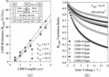
Fig. 1. (a) Relationship between LDD resistance (RLDD) and LDD length. The straight lines are the linear fitting of the RLDDextracted from the poly-Si TFTs with LDD lengths greater than 1.5 µm. The device structure is shown in the inset. (b) Variation ratios of RLDDas a function of gate bias for devices with different LDD lengths are depicted. The variation ratio is the RLDDat different gate biases (VGS= 3 to 15 V) divided by the RLDDat VGS= 3 V.
in the numerical simulation of LDD MOSFETs [6], [7]. However, little experimental evidence can be found since MOSFETs seldom have the LDD length greater than 0.3 µm. In this letter, a 0.55-µm-long channel extension under a 10-V gate bias was first reported. The influences of the gate bias, LDD doping level, gate oxide thickness, and LDD length on the channel extension are also investigated by using Silvaco ATLAS simulation.
II. EXPERIMENTAL
A 50-nm-thick a-Si layer was first deposited on a glass substrate and then crystallized by excimer laser annealing with the laser energy density of 420 mJ/cm2. After the active island formation, a 60-nm-thick oxide layer was deposited as the gate insulator. Next, a 200-nm-thick Molybdenum was de-posited and patterned as the gate electrode. The n−doping was performed self-aligned to the gate electrode by phosphorous implantation with a dosage of 6× 1012 cm−2. The n+ source
and drain regions were defined by an additional mask and doped by phosphorous with a dosage of 1× 1020cm−2. Dopants were activated by thermal process. After the deposition of nitride passivation and the formation of contact holes, a 550-nm-thick aluminum layer was deposited and patterned as the metal pads. All the devices exhibit threshold voltage = 0.55 V and subthreshold swing = 0.31 V/dec. The standard devices with-out LDD structures have a mobility of 94 cm2/Vs. All the
ZAN AND WANG: CHANNEL LENGTH EXTENSION IN POLY-SI TFTs WITH LDD STRUCTURE 1035
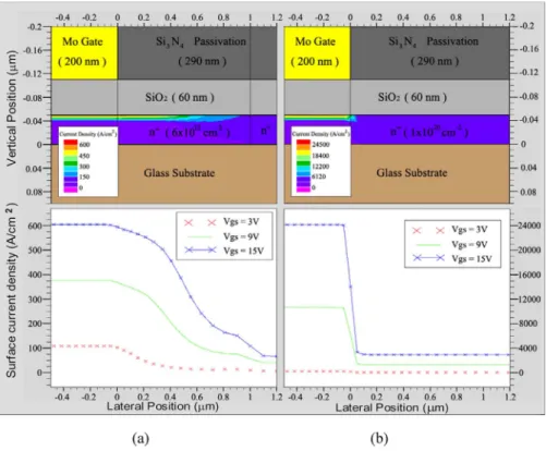
Fig. 2. Current density distribution (VGS= 15 V) and surface current density distribution (VGS= 3, 9, and 15 V) for (a) devices with a 1-µm-long LDD and (b) devices without LDD structures. The channel width is 6 µm, and the channel length is 6 µm. The simulation was performed by Silvaco ATLAS with device structures shown in the inset of Fig. 1(a) and with density-of-states distribution.1
devices exhibit a channel length of 6 µm, a channel width of 6 µm, and an identical distance between the edge of the contact holes and the boundary of the n+/n−regions.
III. RESULTS ANDDISCUSSION
First, the turn-on resistance as a function of gate bias is extracted from the transfer characteristics measured when the drain bias (VDS) is 0.1 V. The resistance is considered to
include an intrinsic channel resistance located under the gate electrode as well as a parasitic resistance caused by the LDD resistance, the n+ sheet resistance, and the contact resistance. When VDS is small, the intrinsic channel resistance of all the
devices should be the same under an identical gate bias. With the aforementioned process control and structure design, the n+
sheet resistance and the contact resistance for all the devices should be the same. As a result, the LDD resistance (RLDD)
can be obtained by subtracting the turn-on resistance of devices without LDD from that of devices with LDD. As shown in Fig. 1(a), RLDD is plotted as a function of LDD lengths under
three gate biases (VGS= 5, 10, and 15 V). When the LDD
length is greater than 1.5 µm, the relationship between RLDD
and the LDD length can linearly be fitted. When the LDD length is 1 or 0.5 µm, however, RLDDdeviates from the fitting lines.
This implies that RLDD has a different resistivity in short and
long LDD lengths. To study the underlying mechanism, the influence of gate bias on RLDDwas analyzed. By taking RLDD
under VGS= 3 V as the reference, the RLDD’s under different
gate biases (VGS= 3 V to 15 V) were normalized and shown in
Fig. 1(b). Obviously, RLDD’s in the short LDD regions suffer
from severe gate modulation effect.
By using the Silvaco ATLAS device simulator with the device structure and the doping dosage shown in the inset of Fig. 1(a), the current density distributions (VGS= 15 V) of
devices with LDD (1 µm) and without LDD structures are shown at the top of Fig. 2(a) and (b). Obviously, the high current density region (channel region) of devices with LDD structures extends into the LDD region, whereas the channel region of devices without LDD structures is well confined by the gate electrode. The surface current density (Jsf) distributions of the
two devices under various gate biases (VGS= 3, 9, and 15 V)
are shown at the bottom of Fig. 2(a) and (b). Devices with LDD structures exhibit an extended channel as a strong function of gate bias.
Then, the extended channel length (∆L) is defined as the distance between the gate edge and the position at which the surface current density (Jsf) is e−1× Jsfmax, where Jsfmax is
the maximum value of Jsf under the given gate bias. Fig. 3(a)
depicts ∆L as a function of gate bias under various LDD doping dosages. ∆L increases with increasing gate bias and saturates under high gate bias. When the LDD doping dosage is below 6× 1012cm−2, it has no influence on ∆L. When the LDD doping dosage increases from 6× 10¹²to 6× 1013cm−2, ∆L gradually reduces to be almost zero. It is noted that the simulation uses the bandgap defect model with the parameters
1Bandgap defect model parameters for acceptor-like states. 1) Expo-nentially distributed tail states: density at the conduction band (NTA) = 1.12× 1021cm−3/eV, and characteristic decay energy (WTA) = 0.02 eV. 2) Gaussian-distributed deep states: total density (NGA) = 6× 1017cm−3,
central energy (EGA) = 0.3 eV below the conduction band, and characteristic decay energy (WGA) = 0.1 eV. The donor-like states are not addressed because they have no influence on n-channel devices.
1036 IEEE ELECTRON DEVICE LETTERS, VOL. 29, NO. 9, SEPTEMBER 2008
Fig. 3. ∆L extracted from the simulated surface current density distribution as a function of gate bias under (a) various LDD doping dosage and (b) various oxide thickness. ∆L is defined as the distance between the gate edge and the position at which the surface current density (Jsf) is e−1× Jmax
sf , where Jmax
sf is the maximum value of Jsfunder the given gate bias.
given in footnote 1. The acceptor-like deep-state total density (NGA) is 6× 1017cm−3. With a dopant activation rate of 33%
given in the simulation, the dosage of 6× 1012 cm−2 corre-sponds to the doping concentration of 4× 1017cm−3, which is close to NGA. For a doping concentration higher than NGA,
the channel extension is significantly suppressed. Three star symbols representing the x-axis intersections of the three fitting lines in Fig. 1(a) are also shown in Fig. 3(a). Their values and relationship with the gate bias are in good agreement with the simulated ∆L. The influence of the gate oxide thickness can be studied by extracting ∆L from the same simulation of Jsf
distri-bution with different oxide thicknesses (60, 100, and 150 nm). As shown in Fig. 3(b), the thinner the oxide thickness, the more pronounced the fringing field and the channel extension.
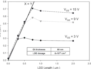
Finally, ∆L as a function of LDD length under VGS= 3, 9,
and 15 V is shown in Fig. 4. When the LDD length is small, ∆L is very close to the LDD length. When the LDD length is large, ∆L tends to saturate and has no dependence on the LDD length. A hump is found in the transition region, and the mechanism needs further investigation. However, it can be noted that when the LDD length is 0.5 µm, the whole LDD region is almost fully occupied by the extended channel.
IV. CONCLUSION
According to the LDD resistance analysis and the device simulation results performed by Silvaco ATLAS, a pronounced channel extension phenomenon has been proposed in poly-Si
Fig. 4. ∆L extracted from the simulated surface current density distribution as a function of LDD length under VGS= 3, 9, and 15 V.
TFTs with LDD structures. The fringing field from the gate induces the channel in the LDD region, whereas no such effect can be observed for devices without LDD structures. The extended channel length is strongly influenced by the gate bias, oxide thickness, and LDD doping concentration when the doping concentration is around the total deep state density (NGA).
REFERENCES
[1] S. D. Brotherton, J. R. Ayres, and M. J. Trainor, “Control and analysis of leakage currents in poly Si thin-film transistors,” J. Appl. Phys., vol. 79, no. 2, pp. 895–904, Jan. 1996.
[2] C. A. Dimitriadis, M. K. Kimura, M. Miyasaka, S. Inoue, F. V. Farmakis, J. Brini, and G. Kamarinos, “Effect of grain boundaries on hot-carrier induced degradation in large grain polysilicon thin-film transistors,” Solid State Electron., vol. 44, no. 11, pp. 2045–2051, Nov. 2000.
[3] Y. Toyota, T. Shiba, and M. Ohkura, “A new model for device degra-dation in low-temperature n-channel polycrystalline silicon TFTs under AC stress,” IEEE Trans. Electron Devices, vol. 51, no. 6, pp. 927–933, Jun. 2004.
[4] A. Bonfiglietti, M. Cuscuna, A. Valletta, L. Mariucci, A. Pecora, F. Gortunato, S. D. Brotherton, and J. R. Ayres, “Analysis of electrical characteristics of gate overlapped lightly doped drain (GOLDD) polysil-icon thin-film transistors with different LDD doping concentration,” IEEE Trans. Electron Devices, vol. 50, no. 12, pp. 2425–2433, Dec. 2003. [5] Y. C. Wu, T. C. Chang, P. T. Liu, C. S. Chen, C. H. Tu, H. W. Zan, Y. H. Tai,
and C. Y. Chang, “Effects of channel width on electrical characteristics of polysilicon TFTs with multiple nanowire channels,” IEEE Trans. Electron Devices, vol. 52, no. 10, pp. 2343–2346, Oct. 2005.
[6] Y. Taur, “MOSFET channel length: Extraction and interpretation,” IEEE Trans. Electron Devices, vol. 47, no. 1, pp. 160–170, Jan. 2000.
[7] J. Y.-C. Sun, M. R. Wordeman, and S. E. Laux, “On the accuracy of channel length characterization of LDD MOSFETs,” IEEE Trans. Electron Devices, vol. ED-33, no. 10, pp. 1556–1562, Oct. 1986.