Characterization of multilayered Ti/TiN ®lms grown by chemical vapor
deposition
J.C. Hu
a, T.C. Chang
b,*, L.J. Chen
a, Y.L. Yang
b, C.Y. Chang
caDepartment of Materials Science and Engineering, National Tsing Hua University, Hsinchu 300, Taiwan bNational Nano Device Laboratory, Hsinchu 300, Taiwan
cDepartment of Electronics Engineering and Institute of Electronics, National Chiao Tung University, Hsinchu 300, Taiwan
Abstract
The resistivity of multilayered Ti/TiN ®lms grown by chemical vapor deposition can be reduced from 240 mV cm (standard sample) to 120 mV cm with NH3plasma post-treatment for 300 s. Increasing the number of multilayered Ti/TiN ®lms of reduced thickness and a plasma
post-treatment technique contributed to reducing the resistivity of TiN ®lms effectively. Smooth multilayered Ti/TiN ®lms were observed by XTEM image. The content of chlorine in the multilayered Ti/TiN ®lm was 1.6 at.%. Therefore, corrosion in the subsequent Al ®lm should be minimized. SIMS depth pro®les of the multilayered Ti/TiN sample showed that Ti atom distribution is fairly uniform. The result is in agreement with the observation of XTEM and the measurement of AES depth pro®les. The resistivity of multlayered Ti/TiN ®lms can be further reduced to 75 mV cm with an in situ NH3plasma post-treatment (500 W) for 300 s followed by RTA at 9008C for 60 s. Therefore, low
resistivity (,100 mV cm) and low Cl concentration (,2 at.%) CVD TiN ®lms can be achieved by a combination of forming a multilayered Ti/TiN structure, and using NH3plasma post-treatment and RTA. q 1998 Elsevier Science S.A. All rights reserved.
Keywords: Multilayered Ti/TiN ®lm; Plasma post-treatment; PECVD Ti; LPCVD TiN
1. Introduction
The microelectronics industry has shown an increasing interest in CVD TiN because of its high thermal stability, low electrical resistiviy, and good diffusion barrier charac-teristics [1±3]. As the device dimensions scale down to deep submicron level, the limitation of ®lms produced by physi-cal vapor deposition has become apparent. Low pressure chemical vapor deposition (LPCVD) of TiN ®lms provided excellent step coverage and uniformity [4,5], even for 0.5 mm or smaller contact windows. The improved feature was attributed to favorable surface controlled reactions.
Two organometallic precursors of tetrakis dimethyl amino titanium (TDMAT) and tetrakis diethyl amino tita-nium (TDEAT) [6,7] were commonly used to deposit MOCVD TiN ®lm. However, deposition of MOCVD TiN by thermal decomposition of TDMAT and TDEAT resulted in high carbon content, which was dif®cult to eliminate. Thus, the resistivity of MOCVD-TiN ®lm was too high. By using TiCl4 and NH3as reactants with N2 as a dilute
gas, CVD-TiN ®lms could be used as a diffusion barrier for Al interconnects and an adhesion layer for W-plugs.
In TiCl4/NH3based CVD-TiN process, the incorporation
of chlorine (Cl) in the ®lm is of major concern for long-term reliability of the ®nished device. Suzuki et al. [8] reported that a higher deposition temperature (.6008C) could reduce Cl concentration in a conventional thermal CVD-TiN ®lm. Hence, LPCVD TiN ®lm can be used as a barrier layer between Si and Al interconnections. Furthermore, in order to reduce chlorine content of TiN ®lms, an in situ NH3
plasma post-treatment technique was applied [9]. As a result, the resistivity of TiN ®lm can be reduced to 133 mV cm by in situ NH3plasma post-treatment. In a previous
study [10], rapid thermal annealing (RTA) of TiN was found to induce little grain growth, but promote sintering to elim-inate grain boundary voids.
In the present work, a combination of mutilayered Ti/TiN and plasma post-treatment technique was found to reduce the resistivity and concentration of chlorine in TiN ®lms. In addition, mutilayered Ti/TiN ®lms processed by RTA were also characterized.
2. Experimental procedures
Single crystal, 15±25 V cm, 6-inch in diameter, p-type (001) oriented silicon wafers were used in this work. The wafers were ®rst chemically cleaned by a conventional wet
0040-6090/98/$ - see front matter q 1998 Elsevier Science S.A. All rights reserved. PII S0040-6090(98)01018-9
* Corresponding author Tel.:1886 3 5726100 X7710; fax:100 886 3 5713403; e-mail: [email protected].
cleaning process. After initial cleaning, the wafers were dipped in a dilute HF solution (HF/H2O, 1:50) immediately
before loading into a deposition chamber. The base vacuum level of the CVD chamber was maintained to be better than 1026 Torr. Plasma-enhanced chemical vapor deposition
(PECVD) Ti and low-pressure chemical vapor deposition (LPCVD) TiN were deposited on the Si substrate in sequence. Ti ®lms were deposited by PECVD using TiCl4
and H2as reactants and the total pressure was 5 Torr. The RF
power was 500 W. On the other hand, TiN ®lms were depos-ited by LPCVD using TiCl4 and NH3as reactants and the
total pressure was 20 Torr when LPCVD TiN ®lm was deposited. All the ®lms were deposited by CVD processed in a Materials Research Corporation (MRC) multichamber cluster tool. The substrate temperature during both Ti and TiN ®lm growth was maintained at 6308C. The in situ NH3
plasma post-treatment was applied to as-deposited
multi-annealed for 60 s in the temperature range of 650 to 9008C by RTA in N2ambient.
Transmission electron microscopy (TEM) and X-ray diffractometry (XRD) were applied to investigate the micro-structure and crystal orientation of TiN ®lms. Auger elec-tron spectroscopy (AES) was used to determine the stoichiometry and uniformity along the depth direction. Secondary ion mass spectrometry (SIMS) was employed to characterize prepared samples. A four-point probe detec-tor was used to measure the resistivity of samples with thickness 46 nm.
3. Results and discussion
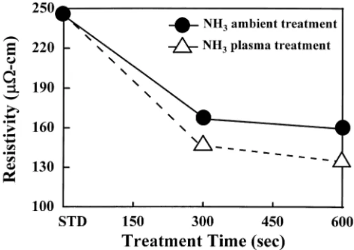
PECVD Ti and LPCVD TiN were deposited on the Si substrate in sequence. Fig. 1 shows the resistivity of these multilayered samples as a function of the two post-treat-ments time. The resistivity of these samples decreased with the time of NH3 post-annealing and NH3 plasma
post-treatment. The resistivity of these ®lms was reduced from 240 to 133 mV cm after NH3plasma-treatment for 600
s. However, the resistivity of these ®lms was only reduced to 160 mV cm after thermal annealing in NH3ambient.
There-fore, in situ NH3plasma post-treatment was more effective
in reducing the resistivity of TiN ®lms [9]. In addition, selective NH3 plasma post-treatment for 300 s can save
processing time. For the investigation of mutilayered Ti/ TiN ®lms, PECVD Ti and multilayered Ti/TiN were also deposited on the Si substrate in sequence. The substrate temperature during Ti and TiN ®lm growth was also main-tained at 6308C. A 9.5-nm thick TiSi2thin ®lm was formed
during the deposition of PECVD Ti on Si. Then a 46-nm thick mutilayered Ti/TiN thin ®lm was deposited on TiSi2/
Si. Both in situ NH3post-annealing and in situ NH3plasma
post-treatment for 300 s were carried out to reduce Cl and compensate N concentration in multilayered Ti/TiN ®lms. Fig. 2 shows the resistivity of these samples as a function of the number of layers. The resistivity of these samples was decreased with the number of Ti/TiN layers. The resistivity of these multilayered Ti/TiN ®lms can be reduced from 240 (STD) to 120 mV cm (III) with NH3plasma-treatment for Fig. 1. The resistivity as a function of the post-treatment time for samples
with different treatment methods. The thickness of these samples is 46 nm.
Fig. 2. The resistivity of various samples with different treatments. They are treated by in situ NH3ambient or NH3plasma post-treatment for 300 s.
Samples are labeled as follows: (STD): TiN/TiSi2/Si, as a standard treated
by in situ NH3ambient post-treatment for 30 s; (I): TiN/Ti/TiN/TiSi2/Si,
(II): TiN/Ti/TiN/Ti/TiN/TiSi2/Si and (III): TiN/Ti/TiN/Ti/TiN/Ti/TiN/
300 s. Therefore, increasing the number of multilayered of Ti/TiN ®lms and utilizing the plasma post-treatment tech-nique contributed to reduce the resistivity of TiN ®lms.
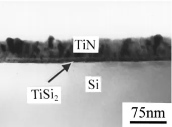
A cross-section TEM image of TiN ®lm treated by NH3
plasma for 600 s is shown in Fig. 3. The interfaces of TiN/ TiSi2/Si structure are seen to be rather smooth. Fig. 4 shows
a plan-view micrograph. The average grain size of TiN ®lm was measured to be about 20 nm. For multilyered Ti/TiN ®lms, a cross-section TEM image of TiN/Ti/TiN/Ti/TiN/Ti/ TiN/TiSi2/Si sample was treated by an in situ NH3plasma
post-treatment for 300 s which was labeled as sample (III). The interfaces of multilayered Ti/TiN/TiSi2/Si are also seen
to be rather smooth as seen in Fig. 5. However, the inter-faces of multilayered Ti/TiN in TiN ®lms are not apparent in the XTEM image. It is believed that Ti atoms are distributed fairly uniformly by fast diffusion in TiN ®lms. A plan-view micrograph is shown in Fig. 6. The average grain size of mutilayered Ti/TiN ®lm was also about 20 nm.
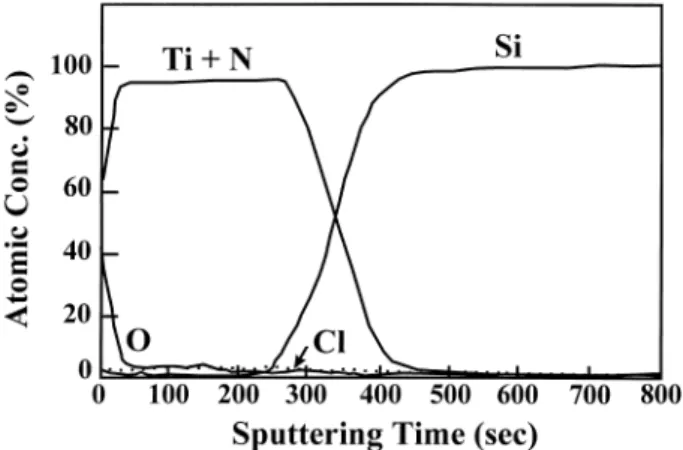
Fig. 7 shows the AES depth pro®le of a TiN/TiSi2/Si
sample after NH3 ambient post-treatment for 30 s. The
concentration of Cl in the sample was found to be about 3 at.%. Therefore, the sample STD had a higher value of resistivity (,240 mV cm). In contrast, Fig. 8 reveals the AES depth pro®le of TiN/Ti/TiN/Ti/TiN/Ti/TiN/TiSi2/Si
sample after being treated by NH3 plasma post-treatment
for 300 s. The concentration of Cl in the sample was found to be about 1.6 at.%, which was lower than that of the sample STD. A previous study showed that chlorine content in excess of 5 at.% would degrade metal reliability and increase the resistivity of the TiN ®lm [11]. The content of chlorine in the multilayered Ti/TiN ®lm was chosen to be 1.6 at.%. Therefore, corrosion in subsequent Al ®lm should be eliminated. In addition, the concentration of Ti1N was
Fig. 3. XTEM image of a CVD-TiN/TiSi2/Si sample treated by in situ NH3
plasma post-treatment for 600 s. The RF power of NH3plasma was 500 W.
The thickness of the CVD-TiN sample is 46 nm.
Fig. 4. Plan-view image of a CVD-TiN sample treated by in situ NH3
plasma post-treatment for 600 s. The RF power of NH3plasma was 500
W. The thickness of the CVD-TiN sample is 46 nm.
Fig. 6. Plan-view image of a multilayered TiN/Ti/TiN/Ti/TiN/Ti/TiN/ TiSi2/Si sample treated by in situ NH3plasma post-treatment for 300 s.
The RF power of NH3plasma was 500 W. The thickness of the multilayered
Ti/TiN sample is 46 nm.
Fig. 5. XTEM image of a multilayered TiN/Ti/TiN/Ti/TiN/Ti/TiN/TiSi2/Si
sample treated by in situ NH3plasma post-treatment for 300 s. The RF
power of NH3plasma was 500 W. The thickness of the multilayered Ti/TiN
fairly uniformly in the TiN/Ti/TiN/Ti/TiN/Ti/TiN/TiSi2/Si
sample by AES measurement.
To investigate Ti atom distribution behavior in multi-layered Ti/TiN ®lms in detail, the 47Ti1N and 51Ti depth
pro®les were measured by SIMS for an as-deposited multi-layered TiN/Ti/TiN/Ti/TiN/Ti/TiN/TiSi2/Si sample as
shown in Fig. 9. It can be seen that the distribution of Ti atoms is fairly uniform in the multilayered Ti/TiN sample. The result is in agreement with the observation of XTEM and the measurement of AES depth pro®le shown in Fig. 5 and Fig. 6. On the other hand, a previous study showed that the PECVD Ti deposition rate varied with different substrate [12]. Except for amorphous and crystal Si, the deposition rate of PECVD Ti is rather low on other substrates. Owing to the TiCl4etching characteristics, deposition and etching
behavior can occur simultaneously for PECVD Ti deposited on TiN ®lms. As a result, the thickness of PECVD Ti depos-ited on TiN for 20 s to form multilayered Ti/TiN ®lms is relatively thin. Furthermore, the Ti atoms are fairly uniformly distributed by fast diffusion in TiN ®lms. In addi-tion, the very thin layer of PECVD Ti deposited on TiN may
also ®ll the grain boundary of TiN ®lm to improve resistiv-ity.
Fig. 10 shows the resistivity of these multilayered Ti/TiN samples as a function of RTA temperature in samples annealed for 60 s. The resistivity of these multlayered TiN/Ti/TiN/Ti/TiN/Ti/TiN/TiSi2/Si samples can be reduced
to 75 mV cm with a NH3plasma post-treatment for 300 s
followed by RTA at 9008C for 60 s. However, the resistivity of TiN ®lms STD was only reduced to 150 mV cm with annealing in a NH3ambient post-treatment for 30 s followed
by RTA at 9008C for 60 s. A previous study [10] showed that the RTA-induced grain sintering results in a tighter grain boundary structure and thus enhances the TiN barrier properties, which is of great importance for the sub-0.25 mm technology with Al plug or Cu metallization. In addition, XRD peaks of multilayered TiN/Ti/TiN/Ti/TiN/Ti/TiN/ TiSi2/Si ®lm reveal a polycrystalline phase of NaCl type
is seen in Fig. 11. A stronger (002) and a weak (111) peak
Fig. 7. The AES depth pro®le of a CVD-TiN/TiSi2/Si sample after being
treated by in situ NH3ambient post-treatment for 30 s.
Fig. 8. The AES depth pro®le of a multilayered TiN/Ti/TiN/Ti/TiN/Ti/ TiN/TiSi2/Si sample treated by in situ NH3plasma post-treatment for 300 s.
Fig. 10. The resistivity of various samples as a function of RTA tempera-ture for 60 s. Samples are labeled as follows: (STD): TiN/TiSi2/Si, as a
standard treated by in situ NH3ambient post-treatment for 30 s; (I): TiN/Ti/
TiN/TiSi2/Si, (II): TiN/Ti/TiN/Ti/TiN/TiSi2/Si and (III): TiN/Ti/TiN/Ti/
TiN/Ti/TiN/TiSi2/Si. They were treated by in situ NH3ambient or NH3
plasma post-treatment for 300 s.
Fig. 9. The SIMS depth pro®le of a multilayered TiN/Ti/TiN/Ti/TiN/Ti/ TiN/TiSi2/Si sample treated by in situ NH3plasma post-treatment for 300 s.
in XRD spectrum of multilayered TiN/Ti/TiN/Ti/TiN/Ti/ TiN/TiSi2/Si ®lm by RTA at 9008C for 60 s were observed.
Due to grain growth, the intensity of (002) and (111) peaks of the XRD spectrum of multilayered TiN/Ti/TiN/Ti/TiN/ Ti/TiN/TiSi2/Si ®lm increased with RTA temperature. Fig.
12 shows the grain structure of multilayered TiN/Ti/TiN/Ti/ TiN/Ti/TiN/TiSi2/Si ®lm after RTA at 9008C for 60 s. The
average grain size was measured to be about 35 nm which is larger than that of as-deposited mutilayered TiN/Ti/TiN/Ti/ TiN/Ti/TiN/TiSi2/Si ®lm (20 nm). As a result, low
resistiv-ity (,100 mV cm) and low Cl concentration (,2 at.%) of CVD TiN ®lms can be achieved by a combination of form-ing multilayered Ti/TiN structure, NH3plasma
post-treat-ment and RTA. 4. Conclusions
The resistivity of multilayered Ti/TiN ®lms can be reduced from 240 cm (standard sample) to 120 mV cm with NH3plasma post-treatment for 300 s. Increasing the
number of multilayered Ti/TiN ®lms and the use of the plasma post-treatment technique contributed to reduce the resistivity of TiN ®lms effectively. Smooth multilayered Ti/ TiN ®lms were observed by XTEM image. The content of chlorine in the multilayered Ti/TiN ®lm was 1.6 at.%. Therefore, corrosion in the subsequent Al ®lm should be minimized. SIMS depth pro®les of the multilayered Ti/ TiN sample showed that Ti atom distribution is fairly uniform. This result is in agreement with the observation of XTEM and the measurement of AES depth pro®le. The resistivity of multlayered Ti/TiN ®lms can be further reduced to 75 mV cm with a NH3 plasma post-treatment
for 300 s followed by RTA at 9008C for 60 s. Therefore, low resistivity (,100 mV cm) and low Cl concentration
(,2 at.%) of CVD TiN ®lms can be achieved by a combina-tion of forming multilayered Ti/TiN structure, and using NH3plasma post-treatment and RTA.
Acknowledgements
The work was supported by National Nano Device Laboratory and National Science Council of the People's Republic of China under contract nos. NSC87-2215-E317-002 and NSC87-2721-2317-200.
References
[1] R.I. Hedge, R.W. Fiordalice, E.O. Travis, R.J. Tobin, J. Vac. Sci. Technol. B 11 (1993) 1287.
[2] J.S. Byun, C.R. Kim, K.G. Rha, J.J. Kim, Jpn. J. Appl. Phys. 34 (1995) 978.
[3] J.T. Hillman, R. Foster, J. Faguet, W. Triggs, R. Arora, M. Ameen, Solid State Technol. (1995) 147.
[4] J.T. Hillman, Proc. SEMI Taiwan Tech. Conf, Taiwan p. (1995) 8. [5] J. Faguet, C. Arena, E. Guidotti, R.F. Foster, J.T. Hillman, Advanced
Metallization for ULSI Applications in 1995. Mater. Res. Stand., 1995, p. 259.
[6] A. Paranipe, M.L. Raja, J. Vac. Sci. Technol. B 13 (1995) 2105. [7] S.C. Sun, M.H. Tsai, Thin Solid Films 253 (1994) 440.
[8] T. Suzuki, T. Ohba, Y. Furumura, H. Tsutikawa, Proc. 10th Int. VLSI Multilevel Interconnection Conf., IEEE, New York, 1993 p. 418. [9] Y.J. Mei, T.C. Chang, J.C. Hu, et al., Thin Solid Films 308 (1997)
594.
[10] X.W. Lin, S. Bothra, L. Topete, D. Pramanik, 14th Int. VLSI Multi-level Interconnection Conf., 1997 p. 443.
[11] T. Kaizuka, H. Shinriki, N. Takeyasu, T. Ohta, Jpn. J. Appl. Phys. 33 (1994) 470.
[12] T. Taguwa, K. Urabe, K. Ohto, H. Gomi, 14th Int. VLSI Multilevel Interconnection Conf., 1997 p. 255.
Fig. 12. Plan-view image of multilayered a TiN/Ti/TiN/Ti/TiN/Ti/TiN/ TiSi2/Si sample treated by in situ NH3plasma post-treatment for 300 s
followed by RTA at 9008C for 60 s. Fig. 11. XRD spectra of multilayered TiN/Ti/TiN/Ti/TiN/Ti/TiN/TiSi2/Si
samples treated by in situ NH3plasma post-treatment for 300 s followed by