0925-9635/03/$ - see front matter䊚 2003 Elsevier Science B.V. All rights reserved. doi:10.1016/S0925-9635(03)00181-X
sources in a microwave plasma chemical vapor deposition system(MPCVD). Doping boron causes the growth rate of CNTs to decrease. This might be due to the high oxygen content contained in the doping source that induces oxidation of graphite. The bamboo-like nanostructure of the carbon tubes disappeared with boron doping. Raman spectrum shows the higherI yI ratio inD G boron-doped CNTs. This implies the decrease of graphitization in boron-doped CNTs. In addition, doping boron could enhance the field emission property by increasing the current density by more than 30%(from 350 to 470 mAycm at 2.2 Vymm).2 䊚 2003 Elsevier Science B.V. All rights reserved.
Keywords: Nanotubes; p-Type doping; Chemical vapor deposition; Field emission
Table 1
Deposition conditions
Sample Flow rate
CH4yH qdoping source2 (sccm)
A(undoped) 10y40
B(boron-doped) 10y40q0.5 C(boron-doped) 10y40q1 D(boron-doped) 10y40q2
Note: Deposition times10 min; Total pressures15 torr; MW
pow-ers400 W; Substrate temp. (8C)s;700; Doping source: B(OCH ) .3 3
1. Introduction
Since their first discovery in 1991 w1x, carbon nano-tubes (CNTs), have been considered for various appli-cations. Their small dimension, high strength and the remarkable physical properties(like high Young’s mod-ulus and high-aspect ratio) of these structures make them very promising emitters for field emission devices. Due to the size-effect and structure diversity of nan-omaterials, the physical properties strongly depend on their micro structure, size and chemical bonding w2x. Different diameter, length and chirality of CNTs gives rise to diverse physical and mechanical properties. In general, for a semiconductor field emitter, the emitting electrons can originate from the conduction band, the valence band andyor surface states. It is believed that the inclusions such as nitrogen, phosphorus or boron can enhance CNTs’ electron properties by offering electrons or holes.
Boron-doped CNTs are predicted to act as semicon-ductors among large range diameters and chiralities. Boron-doped CNTs(ByC ratio-0.05) were reported as by-products when BC N CNTs were prepared by an arc-2
discharge method w3x. Recently, we have successfully *Corresponding author. Tel.: 935889532; fax: q886-62616193.
E-mail address: [email protected](C.L. Tsai).
synthesized boron-doped diamond-like emitters in microwave plasma chemical vapor deposition (MPCVD) w4x. In this article, selective area deposition (SAD) of boron-doped CNTs was directly completed in MPCVD.
2. Experiment
The starting substrates were mirror-polish n-type, (100) oriented Si wafer with a resistivity of 4.5;5.5 Vycm. Wafers were cleaned by Radio Corporation of America (RCA) cleaning process to remove contami-nation on the silicon surface. After cleaning, a SiO2
dielectric layer was deposited using high-temperature and low-pressure furnace deposition system (model
Fig. 1. SEM photographs of(a) undoped and (b) boron-doped CNTs array.
Fig. 2. TEM images of undoped CNTs. ASM LB-45). A pattern of 8 mm wide dots with 8 mm
space between them was successfully fabricated onto a photoresist layer using ASM PAS 2500y10 G-Line exposer and the Convac CPP-70 developing system. A 150-nm-thick film of Fe catalyst was deposited on
SiO by using dual E-Gun evaporator2 (model ULVAC EBX-10C, Japan). Then, the photoresist was removed by lift-off process in an acetone solution in an ultrasonic agitator. Finally, the patterned substrates were put in a microwave plasma chemical vapor deposition
Fig. 3. TEM images of(a) sample C and (b) sample D.
(MPCVD) chamber to grow selective patterned deposi-tion (SAD) of CNTs. The reactive gases used in depo-sition were CH –H with flow rate of 10y40 sccm and4 2
trimethylborate B(OCH ) as doping source with 0.5; 13 3
and 2 sccm, respectively. The average deposition time and substrate temperature were 10 min and 700 8C measured by pyrometer. Table 1 lists the experimental conditions.
The length and the morphology of the produced CNTs were characterized by scanning electron microscopy (SEM). A transmission electron microscopy (TEM) was used to determine the nanostructure of individual CNT. The TEM specimens were prepared by dispersing the CNTs in an acetone ultrasonic bath. A drop of the suspension was placed onto a carbon lace film Cu grid. Raman spectroscopy was used to evaluate the crystallin-ity. Secondary ion mass spectrometry(SIMS) was used
to detect the amount of boron. AnI–V measuring system
was used to obtain the field emission property.
3. Results and discussion
3.1. Scanning electron microscopy(SEM)
Fig. 1a and b show the SEM pictures of undoped and boron-doped CNTs, respectively. The photograph on the right side of each figure is an enlarged image. Eight micrometer-bound aligned CNTs are successfully com-pleted through selective area deposition method. Obvi-ously, it is found that the undoped CNTs are longer length. Under the SEM analysis, we find that undoped CNTs are denser than boron-doped ones. This could be explained by the high oxygen content contained in the B(OCH ) . High concentration of oxygen increases the3 3
Fig. 4. Raman spectrum of undoped and various concentrations of boron-doped CNTs.
Fig. 5.I yI ratio of undoped and various concentrations of boron-D G
doped CNTs.
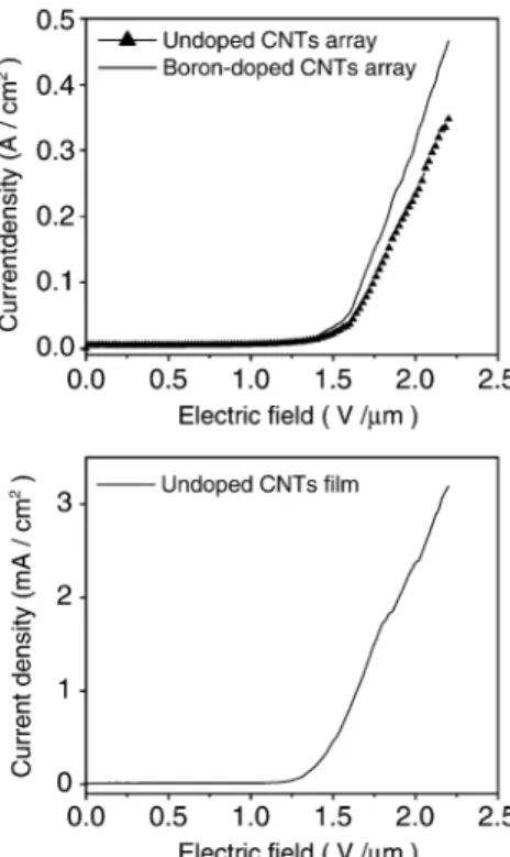
Fig. 6. Current density(J)–electric field (E) curve of undoped CNTs films, undoped and boron-doped CNTs arrays.
etching rate during CNTs growth under 700 8C. This is in accordance with our previous study, where the growth of diamond was inhibited when O was added to the2
CH –CO gas mixture w5x.4 2
3.2. Transmission electron microscopy (TEM)
Figs. 2 and 3 show the TEM images of undoped and boron-doped CNTs, respectively. In Fig. 3, the right side pictures are enlarged images of the ones on the left. Based on TEM images, the diameter of undoped and boron-doped CNTs are approximately 50 nm and 40 nm, respectively. This indicates that boron-doped CNTs have smaller diameter than undoped ones. It is found that undoped CNTs have a bamboo-like shape. This shape has been reported in many studies where the Fe catalyst has been used w6–8x. Once increasing the concentration of B(OCH ) to 2 sccm, the bamboo3 3
structure disappears. In addition, Fig. 3b also shows large amount of amorphous carbon on the CNTs. SIMS results not shown here also verify the existence of boron in the nanotubes.
3.3. Raman spectroscopy
The produced CNTs were also studied by Raman spectroscopy. Raman measurements were performed using a 532-nm Ar laser with 1 cmy1 resolution; integration times were 1 min at 30 mW laser power. Fig. 4 shows the Raman spectrum of undoped and
boron-doped CNTs. All of them have two sharp peaks located at approximately 1350 cmy1 and 1580 cmy1, respectively. The first-order Raman spectrum of CNTs shows strong sharp peaks at 1581 cmy1(G line), which is the high-frequency E g first-order mode and 13502
cmy1 (roughly corresponding to the D line associated with disorder-allowed zone-edge modes of graphite). The 1350 cmy1band is normally explained by relaxation of the wave vector selection rule due to the effect of the finite size of the crystal in the material w9,10x. The other conspicuous phenomenon is that the intensity of D line increases with the increasing concentration of
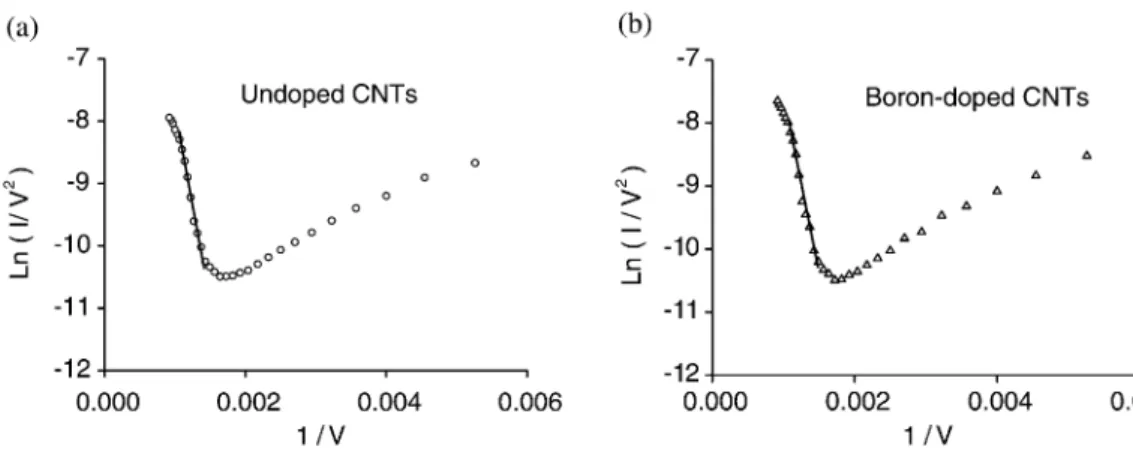
Fig. 7. F–N plot of(a) undoped and (b) boron-doped CNTs arrays.
boron. Normally, the I yID G ratio increases with (i) increasing the amount of amorphous carbon in the material and (ii) decreasing the graphite crystal size. Fig. 5 indicates theI yI ratio increases with increasingD G
the boron concentration. This implies that doping boron decreases the graphitization. Thus, the boron-doping effect strongly influences the crystallinity of CNTs. This result is also consistent with the previous TEM images.
3.4. I–V measurement
The field emission tests are performed on a diode structure, in which the CNTs are separated from the 25 cm indium-tin-oxide anode using 500 mm glass spacers.2
The anode current is measured as a function of anode-to-cathode voltage in a vacuum of 10y6 Torr. The voltage is applied from 0 to 1100 V in steps at 10 V by using the Keithley SMU 237 system. Fig. 6 presents the current density vs. electric field plots for undoped and boron-doped CNTs array as well as undoped CNTs film grown in the same manner without patterning the cata-lyst layer. Obviously, the emitted current density for undoped CNTs array (350 mAycm at 2.2 Vymm) is2
much higher than for undoped CNT films (3.2 mAy cm at 2.2 Vymm2 ). This is a result of the screening effect w11,12x provoked by the proximity of neighboring CNTs. Besides, boron-doping also improves the field emission characteristics of CNT arrays by a 35% increase in the emitted current density from 350 to 470 mAycm at 2.2 Vymm. The respective Fowler–Nord-2
heim (FN) plot (ln(IyV ) vs. 1yV) are shown in Fig.2
7. Plotting ln(IyV ) vs. 1yV results in a straight line for2
applied voltage higher than 700 V, implying the field emission characteristics of CNTs.
4. Conclusion
In this article, we synthesized boron-doped CNTs by using trimethlborate B(OCH ) as doping source. Exper-3 3
imental results show that undoped CNTs possess higher growth rate than boron-doped ones. In addition, the nanostructure of bamboo-like shape disappears in boron-doped CNTs. The I yI ratio increases with increasingD G
concentration of boron, implying the decrease of graph-itization in boron-doped CNTs. Doping boron clearly enhances the emission current density by 35% increase.
Acknowledgments
The authors would like to thank the National Science Council of the Republic of China for financially sup-porting this research under Contract No. NSC 91-2216-E-009-030.
References
w1x S. Iijima, Nature(London) 354 (1991) 56.
w2x Z.L. Wang, in: Z.L. Wang(Ed.), Characterization of Nanophase Materials, Wiley-VCH, New York, 1999, pp. 1–400.
w3x Ph. Redlich, J. Loeffler, P.M. Ajayan, J. Bill, F. Aldinger, M. Ruhle, Chem. Phys. Lett. 260(1996) 465.
w4x C.L. Tsai, C.F. Chen, C.L. Lin, J. Appl. Phys. 90(2001) 4847. w5x C.F. Chen, T.M. Hang, H.C. Chen, J. Appl. Phys. 74(1993)
4483.
w6x W. Xianbao, H. Wenping, L. Yunqi, L. Chenfeng, X. Yu, Z. Shuqin, et al., Carbon 39(2001) 1533.
w7x L.C. Jin, L.S. Chul, K. Hyoun-Woo, L.J. Ho, C.K. Ik, Chem. Phys. Lett. 359(2002) 115.
w8x L. De-Chang, D. Liming, H. Shaoming, W.H.M. Albert, L.W. Zhong, Chem. Phys. Lett. 316(2000) 349.
w9x F. Tuinstra, J.L. Koenig, J. Chem. Phys. 53(1970) 1126. w10x R.J. Nemanich, S.A. Solin, Phys. Rev. B20(1979) 392. w11x P.G. Collins, A. Zettl, Phys. Rev. B55(1997) 9391. w12x O. Groning, O.M. Kuttle, C. Emmenegger, P. Groning, L.