Characterization of C F 4 -plasma fluorinated Hf O 2 gate dielectrics with TaN metal
gate
Chao Sung Lai, Woei Cherng Wu, Jer Chyi Wang, and Tien sheng Chao
Citation: Applied Physics Letters 86, 222905 (2005); doi: 10.1063/1.1944230 View online: http://dx.doi.org/10.1063/1.1944230
View Table of Contents: http://scitation.aip.org/content/aip/journal/apl/86/22?ver=pdfcov
Published by the AIP Publishing
Articles you may be interested in
Combinatorial study of Ni–Ti–Pt ternary metal gate electrodes on Hf O 2 for the advanced gate stack
Appl. Phys. Lett. 89, 142108 (2006); 10.1063/1.2357011
Characterization of field-effect transistors with La 2 Hf 2 O 7 and Hf O 2 gate dielectric layers deposited by molecular-beam epitaxy
J. Appl. Phys. 99, 024508 (2006); 10.1063/1.2163985
Physical and electrical properties of Ta–N, Mo–N, and W–N electrodes on Hf O 2 high- k gate dielectric
J. Vac. Sci. Technol. B 24, 349 (2006); 10.1116/1.2163883
The characteristics of hole trapping in Hf O 2 Si O 2 gate dielectrics with TiN gate electrode
Appl. Phys. Lett. 85, 3525 (2004); 10.1063/1.1808228
3-Ethylindole electronic spectroscopy: S 1 and cation torsional potential surfaces
J. Chem. Phys. 113, 1857 (2000); 10.1063/1.481989
This article is copyrighted as indicated in the article. Reuse of AIP content is subject to the terms at: http://scitation.aip.org/termsconditions. Downloaded to IP: 140.113.38.11 On: Thu, 01 May 2014 03:01:28
Characterization of CF
4-plasma fluorinated HfO
2gate dielectrics with TaN
metal gate
Chao Sung Laia兲
Department of Electronic Engineering,Chang Gung University, 259 Wen-Hwa 1st Road, Kueishan, Taoyuan, Taiwan
Woei Cherng Wu
Department of Electronic Physics, National Chiao Tung University, 1001 Ta Hsueh Rd, Hsinchu, Taiwan
Jer Chyi Wang
Nanya Technology Corporation, Hwa-Ya Technology Park, 669 Fu-Hsing 3rd Rd., Kueishan, Taoyuan, Taiwan
Tien sheng Chao
Department of Electronic Physics, National Chiao Tung University, 1001 Ta Hsueh Rd, Hsinchu, Taiwan
共Received 9 December 2004; accepted 1 May 2005; published online 26 May 2005兲
In this paper, fluorine incorporation into the HfO2gate dielectrics by post CF4plasma treatment was proposed to improve the electrical characterization. TaN–HfO2–p-Si capacitors were demonstrated in this work. The characteristics of fluorinated HfO2gate dielectrics were improved, including the capacitance-voltage hysteresis and current-voltage behaviors. This may be attributed to the fluorine incorporated into the HfO2 gate dielectrics as revealed by secondary ion mass spectroscopy. Moreover, the formation of Hf-F bonding was observed through electron spectroscopy for chemical analysis spectra. © 2005 American Institute of Physics.关DOI: 10.1063/1.1944230兴
An equivalent oxide thickness of less than 1.0 nm will be needed for sub-65 nm MOSFETs 共Metal-Oxide-Semiconductor-Field-Effect-Transistors兲 as illustrated in the International Technology Roadmap for Semiconductors.1 Silicon oxide gate dielectric is now being pushed to both its technological and theoretical limits. The equivalent oxide thickness 共EOT兲 in the 4-Gbit generation dynamic random access memory共DRAM兲 will be scaled down further to 0.22 nm which is very close to the structural limit of silicon di-oxide, as the Si–O bond in silicon oxide is 0.17 nm. The high tunneling leakage current is not acceptable for the scaling of SiO2 below the thickness of 1.0 nm. Numerous attempts in the search for alternate gate dielectrics have been carried out by using hafnium dioxide to replace SiO2as the gate dielec-tric due to its high dielecdielec-tric constant共25–30兲, wide energy bandgap 共⬃5.68 eV兲, and high stability with the Si surface.2–4Unfortunately, for high-k gate dielectrics, there is a hysteresis phenomenon in its capacitance-voltage 共C-V兲 characteristics.5,6 This hysteresis induces a flatband voltage shift, and threshold voltage instability when it is applied to MOSFETs. Therefore, some methods, such as co-sputtering of silicon, and aluminum with hafnium to deposit hafnium silicate and aluminate dielectrics,7,8the use of nitric gas for chemical vapor deposition 共CVD兲9 or oxidizing sputtered metal nitride like HfN10to form hafnium oxynitride共HfON兲 films, and post-deposition NH3 plasma treatment methodology11were used to improve the hysteresis phenom-enon and thermal stability. In this work, we propose a CF4 plasma treatment methodology to investigate its effects on HfO2 gate dielectrics. Leakage current and hysteresis phe-nomenon were much improved for the HfO2 gate dielectrics treated by CF4plasma. The results show that fluorine atoms
were accumulate into the HfO2 dielectrics to form Hf–F bonding by CF4 plasma, resulting in the reduction of gate leakage current, charge trapping, and the hysteresis.
Metal–insulator–semiconductor 共MIS兲 capacitors were fabricated. The starting material for MIS capacitor fabrica-tion is具100典 p-type Si substrate with a resistivity in the range of 10–15⍀ cm. Following the standard cleaning process, an HfO2layer of about 10 nm thick was deposited by reactive sputtering of hafnium metal in oxygen and argon ambient. This thickness is too thick to use as an application of the high-k dielectric in future Si technology. The purpose of us-ing a thicker film at the present stage is for the ease of study-ing both the physical properties of bulk and interface usstudy-ing secondary ion mass spectroscopy共SIMS兲, and electron spec-troscopy for chemical analysis 共ESCA兲. Compared to the control sample共without CF4plasma, denoted as W/O兲, after the gate dielectric deposition, some samples were processed by CF4plasma at 50 W for 1 and 5 min, denoted as P-1 and P-5, respectively. In order to know the thermal stability for the MIS capacitors, post deposition annealing共PDA兲 under the rapid thermal system for 1 min in an N2 ambient at 700 °C was demonstrated for W/O, P-1, and P-5 samples, denoted as W/O/A, P-1/A, and P-5/A, respectively. TaN film of 50 nm was deposited by reactive RF sputter. Thereafter, a 300 nm thick Al film was deposited on the TaN film by thermal evaporator. The gate of the capacitor was defined lithographically and then etched. Finally, a 300 nm thick Al film was deposited on the backside of the wafer to form the ohmic contact. The high frequency 共100 kHz兲 capacitance-voltage 共C-V兲 characteristics and current-voltage 共J-V兲 curves were measured by HP4284 and Keithly 4200, respec-tively, and the effective oxide thickness共EOT兲 was extracted from the high frequency capacitance under the accumulation region without considering the quantum effect. In addition, the fluorine concentration was analyzed by SIMS. The Hf–O a兲Telephone:⫹886-3-2118800, ext 5786; Fax: ⫹886-3-2118507. Electronic
mail: [email protected]
APPLIED PHYSICS LETTERS 86, 222905共2005兲
0003-6951/2005/86共22兲/222905/3/$22.50 86, 222905-1 © 2005 American Institute of Physics
This article is copyrighted as indicated in the article. Reuse of AIP content is subject to the terms at: http://scitation.aip.org/termsconditions. Downloaded to IP: 140.113.38.11 On: Thu, 01 May 2014 03:01:28
and Hf–F bondings were analyzed by ESCA.
The CF4plasma and PDA effects on the current voltage characteristics are shown in Fig. 1. For the CF4 plasma ef-fects, the gate leakage current of the CF4 plasma treated samples 共P-1 and P-5兲 was much smaller than that of the W/O共without plasma兲 sample. The gate leakage current was decreased with the increase in CF4 plasma treatment. The gate leakage current of the HfO2gate dielectrics after 700 °C PDA, was increased due to the crystallization after thermal annealing for HfO2 gate dielectrics, and the resulting grain boundaries are thought to act as significant leakage path-ways. Possible crystallization of HfO2can occur, and when it does it results in an increase in the leakage current for all samples, whether treated by CF4plasma or not. Compared to the as-deposited sample without post-CF4 plasma treatment 共solid triangle markers in Fig. 1, the leakage current at a gate voltage of 2 volts increases three orders after PDA 共open triangle markers兲. However, for the as-deposited samples with post-CF4 plasma 共solid square and circle markers in Fig. 1, the leakage current at gate voltage of 2 volts increased slightly after PDA 共open square and circle markers兲. This was due to the fact that the fluorine incorporation retarded the crystallisation of HfO2gate dielectrics, and improved the thermal stability of the HfO2thin film. In addition, the break-down voltage was also improved for CF4 plasma treated samples 共P-1 and P-5兲. This means that fluorine incorpora-tion into the HfO2 gate dielectrics to strengthens the HfO2 thin film. The normalized C-V hysteresis curves are shown in Fig. 2 for all samples without PDA. According to the inner-interface trapping model,12 majority carriers would trap at the inner-interface of the HfO2 thin film. This phenomenon makes the C-V curve shift during the capacitance-voltage measurement. After CF4plasma treatment, the fluorine atoms were incorporated into the interfacial layer共HfO2–Si inter-face兲 resulting in less charge trapping. The C-V hysteresis was improved with an increasing CF4plasma treatment time. As is evident, the HfO2thin films with CF4plasma treatment at 5 min共P-5兲 showed the smallest C-V hysteresis, of only 10 mV. The inset of Fig. 2 was the Weibull distribution for the magnitude of C-V hysteresis for all samples without PDA. The samples with CF4 plasma treatment showed less
C-V hysteresis, especially for the samples with long CF4
plasma treatment time共sample, P-5兲.
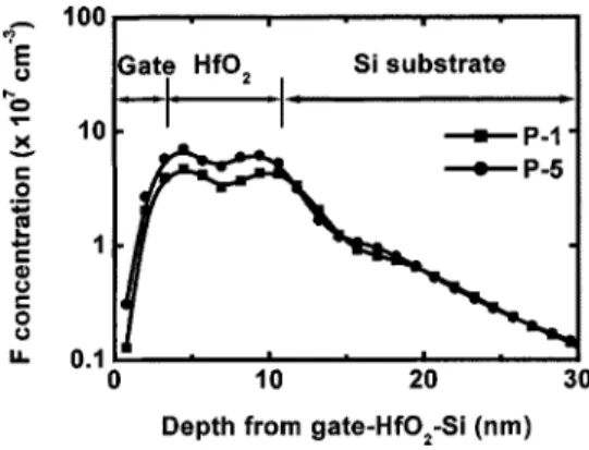
A typical fluorine profile measured by secondary ion mass spectroscopy 共SIMS兲 proves that the fluorine atoms
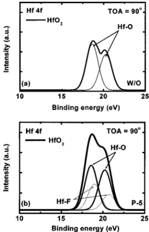
were incorporated into the HfO2 thin films after post- CF4 plasma treatment, as shown in Fig. 3. The amount of the fluorine atoms increased with the increase in CF4 plasma treatment time. In addition, the fluorine atoms showed two peaks in the SIMS analysis, indicating that fluorine atoms almost entirely distributed in the surface of the Si substrate and the interface between the TaN gate and the HfO2 thin film. This phenomenon shows that after post-CF4 plasma treatment, the fluorine atoms would first accumulate at the surface of the HfO2thin film and then diffused through the HfO2thin film to terminate the dangling bond and accumu-late at the interfacial layer between the HfO2 thin film and the Si substrate as illustrated in Fig. 3. However, we still can find some fluorine atoms accumulated in the HfO2thin film, thus we can conclude that the fluorine will distribute in all the HfO2gate dielectrics after CF4plasma treatment. Figure 4 shows the Hf 4f ESCA spectra of the as-deposited and P-5 samples共CF4plasma treated at 5 min兲, respectively. A take-off angle共TOA兲 of 90° was used to measure the ESCA spec-tra. In Fig. 4共a兲, two distinct peaks of the Hf–O bonding at 18.7 and 20.3 eV are evident from the as-deposited sample. The intensity of the Hf 4f of HfO2 dielectrics with CF4 plasma treatment was very high and the original peak value at 20.3 eV was blurry as we can see in Fig. 4共b兲. This phe-nomenon means that there was another Hf bonding forma-tion. Therefore, comparing the Hf–O bonds in Hf 4f spectra of HfO2 gate dielectrics in Fig. 4共a兲 to those of the HfO2 dielectrics with CF4plasma treatment in Fig. 4共b兲 reveals the Hf–F bonding, indicating fluorine incorporation after
post-FIG. 1. The J-V curves共gate leakage current兲 for all samples. The gate leakage current was decreased for the sample with CF4plasma treatment.
The same tendency was evident for the samples with post deposition annealing.
FIG. 2. The normalized C-V hysteresis curves for all samples without PDA. The inset figure is the Weibull distribution for C-V hysteresis. The hysteresis was improved for the sample with CF4plasma treatment.
FIG. 3. The SIMS depth profile of fluorine atoms for all samples. The fluorine atoms distributed in HfO2gate dielectrics and show two peaks in
the interface between TaN–HfO2and HfO2–Si.
222905-2 Laiet al. Appl. Phys. Lett. 86, 222905共2005兲
This article is copyrighted as indicated in the article. Reuse of AIP content is subject to the terms at: http://scitation.aip.org/termsconditions. Downloaded to IP: 140.113.38.11 On: Thu, 01 May 2014 03:01:28
CF4 plasma treatment, as evident from the SIMS profiles in Fig. 3.
An approach to improve the dielectric properties of the HfO2 films by using post-CF4 plasma treatment was pro-posed. The incorporation of fluorine atoms into the HfO2 gate dielectrics improved the characteristics including gate leakage current, breakdown voltage and C-V hysteresis. Af-ter the incorporation of fluorine atoms, the Hf–F bonding formation led to the reduction of charge trapping. The post-CF4plasma treatment technology used in high-k gate dielec-trics is a manufacturing approach for future ULSI applica-tion.
The authors would like to say thank you to the Nanya Technology Corp. This work was supported by the National Science Council of Taiwan, R.O.C., under contract number NSC-92-2218-E-182-008.
1
International Technology Roadmap for Semiconductors共Semiconductors
Industry Association, 2003兲.
2
S. B. Samavedam, L. B. La, J. Smith, S. Dakshina-Murthy, E. Luckowski, J. Schaeffer, M. Zavala, R. Martin, V. Dhandapani, D. Triyoso, H. H. Tseng, P. J. Tobin, D. C. Gilmer, C. Hobbs, W. J. Taylor, J. M. Grant, R. I. Hegde, J. Mogab, C. Thomas, P. Abramowitz, M. Moosa, J. Conner, J. Jiang, V. Arunachalam, M. Sadd, B-Y. Nguyen, and B. White, Tech. Dig. - Int. Electron Devices Meet. 2002, 433共2002兲.
3
B. Tavel, X. Garros, T. Skotnicki, F. Martin, C. Leroux, D. Bensahel, M. N. Semeria, Y. Morand, J. F. Damlencourt, S. Descombes, F. Leverd, Y. Le-Friec, P. Leduc, M. Rivoire, S. Jullian, and R. Pantel, Tech. Dig. - Int. Electron Devices Meet. 2002, 429共2002兲.
4
C. H. Lee, J. J. Lee, W. P. Bai, S. H. Bae, J. H. Sim, X. Lei, R. D. Clark, Y. Harada, M. Niwa, and D. L. Kwong, VLSI Technical Symposium Di-gest 2002, 82共2002兲.
5
K. Kukli, M. Ritala, J. Sundqvist, J. Aarik, J. Lu, T. Sajavaara, M. Leskela, and A. Harsta, J. Appl. Phys. 92, 5698共2002兲.
6
C. M. Perkins, B. B. Triplett, P. C. Mclntyre, K. C. Saraswat, S. Haukka, and M. Tuomminen, Appl. Phys. Lett. 78, 2357共2001兲.
7
M. Koyama, A. Kaneko, T. Ino, M. Koike, Y. Kamata, R. Iijima, Y. Ka-mimuta, A. Takashima, M. Suzuki, C. Hongo, S. Inumiya, M. Takayanagi, and A. Nishiyama, Tech. Dig. - Int. Electron Devices Meet. 2002, 849
共2002兲. 8
W. J. Zhu, T. Tamagawa, M. Gibson, T. Furukawa, and T. P. Ma, IEEE Electron Device Lett. 23, 649共2002兲.
9
C. H. Choi, S. J. Rhee, T. S. Jeon, N. Lu, J. H. Sim, R. Clark, M. Niwa, and D. L. Kwong, Tech. Dig. - Int. Electron Devices Meet. 2002, 857
共2002兲. 10
C. S. Kang, H.-J. Cho, K. Onishi, R. Choi, Y. H. Kim, R. Nieh, J. Han, S. Krishnan, A. Shahriar, and J. C. Lee, Tech. Dig. - Int. Electron Devices Meet. 2002, 865共2002兲.
11
J. C. Wang, D. C. Shie, T. F. Lei, and C. L. Lee, Electrochem. Solid-State Lett. 6 F34共2003兲.
12
J. C. Wang, S. H. Chiao, C. L. Lee, T. F. Lei, Y. M. Lin, M. F. Wang, S. C. Chen, C. H. Yu, and M. S. Liang, J. Appl. Phys. 92, 3936共2002兲.
13
Hiroyuki Ohta, Masaru Hori, and Toshio Goto, Appl. Phys. Lett. 90, 1955
共2002兲.
FIG. 4. Hf 4f ESCA spectra of共a兲 as-deposited sample, and 共b兲 CF4plasma
treated 5 min sample, respectively. A take-off angle共TOA兲 of 90° was used to measure the ESCA spectra.
222905-3 Laiet al. Appl. Phys. Lett. 86, 222905共2005兲
This article is copyrighted as indicated in the article. Reuse of AIP content is subject to the terms at: http://scitation.aip.org/termsconditions. Downloaded to IP: 140.113.38.11 On: Thu, 01 May 2014 03:01:28