Low-temperature fabrication and characterization of Ge-on-insulator
structures
C.-Y. Yu, C.-Y. Lee, and C.-H. Lin
Department of Electrical Engineering, National Taiwan University, Taipei, Taiwan 106, Republic of China and Graduate Institute of Electronics Engineering, National Taiwan University, Taipei, Taiwan 106, Republic of China
C. W. Liua兲
Department of Electrical Engineering, National Taiwan University, Taipei, Taiwan 106, Republic of China and Graduate Institute of Electronics Engineering, National Taiwan University, Taipei, Taiwan 106, Republic of China and National Nano Device Laboratories, Hsiuchu, Taiwan, R.O.C.
共Received 19 December 2005; accepted 22 July 2006; published online 7 September 2006兲 Ge-on-insulator structures have been fabricated by wafer bonding and layer transfer techniques. Ultralow bonding temperatures of 150– 300 ° C are employed in order to suppress hydrogen outdiffusion and to produce a low defect density, in an attempt to produce high photocurrent and photoresponse. Thus reducing the hydrogen outdiffusion results in decreased surface roughness. A low defect density is suggested by a low inversion-current leakage of the tunnel diodes. The photoresponse of the Ge-on-insulator detector is also found to increase with decreasing bonding temperature, indicating that defects caused by hydrogen implantation are passivated more effectively. © 2006 American Institute of Physics. 关DOI:10.1063/1.2347116兴
As channel lengths of metal-oxide-semiconductor field-effect transistors共MOSFETs兲 are deeply scaling down, car-rier mobility enhancement in the channel is desired for im-proving the performance of circuitry. To achieve this purpose, germanium共Ge兲 is a promising channel material for MOSFETs because it has high electron and hole mobilities as compared with Si.1–3A Si-on-insulator structure can improve the performance of complementary metal-oxide semiconduc-tor circuits, due to the reduction of parasitic capacitance. Ge-on-insulator 共GOI兲 structures may thus be particularly suitable for obtaining high-performance MOSFET devices benefiting from both the advantages of mobility enhance-ment and low parasitic capacitance.4,5 The layer transfer technique using wafer bonding and hydrogen implantation 共also called smart cut6,7兲 enables the fabrication of GOI structures. Recently, a GOI structure fabricated by a smart-cut process with low thermal budget 共⬃400 °C兲 has been reported.8In this letter, the fabrication of GOI structures has been demonstrated at⬃150 °C: so far, a lowest GOI process temperature that has been reported. Effects of hydrogen on low-temperature GOI fabrication process have several ad-vantages with smoother cleaved surface and defect passiva-tion beside the low mismatch of thermal expansion reported previously.9
The basic fabrication process of GOI metel-insulator-semiconductor 共MIS兲 detector involves hydrogen ion im-plantation and direct wafer bonding techniques. The Sb-doped n-type Ge substrate 共001兲 is prepared as a “host” wafer. Then, hydrogen ions with a dose of 1⫻1017cm−2and an energy of 200 keV are implanted into the host Ge wafer before bonding to form a deep weakened layer. On the other substrate, thermal oxide with a thickness of 80 nm is grown on the p-type Si substrate to form a “handle” wafer. The handle wafer and the host wafer were hydrophilicly cleaned
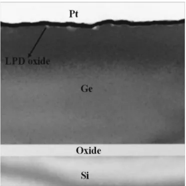
by using NH4OH : H2O2: H2O solution and KOH : H2O solu-tion, respectively. Then, both wafers were rinsed in de-ionized water and initially bonded at room temperature.10,11 The wafer pair was annealed to strengthen the chemical bonds between the two faces and to induce layer transfer along the weakened hydrogen-implanted region by H2 blis-tering. Metal/oxide/Ge tunneling diodes were fabricated for electrical measurements. Low-temperature 共⬃50 °C, lower than the bonding temperature兲 liquid phase deposition 共LPD兲 was used to deposit the gate oxide; this process has the ad-vantages of low cost, selective growth, and high throughput. The thickness of the LPD oxide was⬃1.6 nm. Platinum 共Pt兲 as a gate electrode was evaporated on the LPD oxide and large aluminum共Al兲 pad as an Ohmic contact electrode was evaporated on the same side. A cross-sectional transmission electron micrograph of a GOI metal/oxide/Ge diode is shown in Fig. 1.
The hydrogen can diffuse out from the surface during the bonding process, especially at the instant of breakage. Ac-cording to published experimental result,12hydrogen is a fast diffuser in Ge. A lower process temperature produces a more concentrated hydrogen profile because of the low diffusion coefficient of hydrogen at low temperature. The concentrated hydrogen region would lead to a smooth cleaved surface since the separation along the microcavity plane during the smart-cut process is generated by the hydrogen bubbling near the peak implantation region. Figure 2 shows the sur-face roughness of the GOI sample as a function of process temperatures, measured by atomic force microscopy共AFM兲 on 1⫻1m2 area. The surface roughness continues to de-crease with decreasing process temperature. A root-mean-square 共rms兲 roughness of ⬃7 nm is obtained after the H2 blistering at 150 ° C for 12 h, while the rms roughness is as high as⬃27 nm after blistering at 300 °C for the same time. During thermal treatment, the implanted hydrogen ions can passivate the defects generated by implantation damage in the Ge. At a lower bonding temperature, the outdiffusion
a兲Author to whom correspondence should be addressed; electronic mail:
APPLIED PHYSICS LETTERS 89, 101913共2006兲
0003-6951/2006/89共10兲/101913/3/$23.00 89, 101913-1 © 2006 American Institute of Physics Downloaded 13 Feb 2009 to 140.112.113.225. Redistribution subject to AIP license or copyright; see http://apl.aip.org/apl/copyright.jsp
of hydrogen ions from the wafers can be suppressed and more hydrogen can passivate the defects. Figure 3 shows the tunneling current of Pt/oxide/GOI共MIS兲 diodes as a function of processing temperature. The inset of Fig. 3 is a typical current-voltage curve, for the GOI diode fabricated at 150 ° C. A drop in leakage current was observed for a bond-ing temperature of 150 ° C. The leakage current of MIS tun-neling diodes at inversion bias共negative bias for n-type Ge兲 is dominated by thermal generation of electron-hole pairs through defects in the depletion region and at the Ge/oxide interface共Fig. 4兲.13The lower defect density for the 150 ° C bonding temperature is probably due to the hydrogen passi-vation of defects generated by hydrogen implantation. The wafer holder was cooled down to −20 ° C during the implan-tation process. The heating due to the ion implanimplan-tation may increase the wafer temperature, but the Ge substrate
tempera-ture is estimated to be lower than⬃50 °C. No blistering was observed after the hydrogen implantation in the sample, in-dicating that the wafer temperature is low enough. Due to the equipment limit, the wafer holder temperature cannot be even lower.
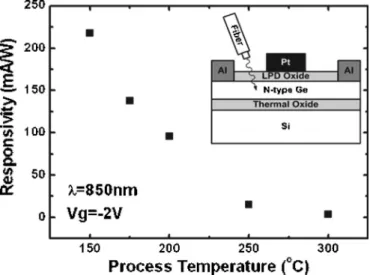
Figure 5 shows the photoresponse of GOI MIS diode under light exposure at a wavelength of 850 nm with differ-ent bonding temperatures.14 The fiber is pointed to the edge of the gate electrode and photogenerated carriers can be col-lected by lateral diffusion and drift mechanisms. The photo-generated holes and electrons in the deep depletion region are separately swept towards the Pt and Al electrodes, re-spectively, to form the photocurrent. The responsivity in-creases from 3.6 to 220 mA/ W as the process temperature decreases from 300 to 150 ° C. Since the Ge surface is pas-sivated by LPD oxide共the inset of Fig. 5兲, the surface current seems to be minimized. Surface defects in GOI near the LPD oxide can act as recombination centers, and the photogener-ated electron-hole pairs can recombine at surface defects, reducing the photocurrent. Therefore, the photocurrent is more sensitive to the surface defects than the dark current. Figure 5 shows a clear trend of decreasing photocurrent with increasing bonding temperature, suggesting a concomitant
FIG. 1. Cross-sectional transmission electron micrograph of GOI MIS detector.
FIG. 2. Surface roughness共rms兲 measured by AFM as a function of process temperature. The surface roughness of the Ge-on-insulator structure de-creases as the process temperature dede-creases 共rms roughness ⬃7 nm at 150 ° C vs⬃27 nm at 300 °C兲.
FIG. 3. Leakage current of a Pt/oxide/GOI detector with different process temperatures at inversion bias of −2 V. Typical current-voltage curves 共in-set兲 for the Ge-on-insulator MIS diode fabricated at ⬃150 °C.
FIG. 4. Band diagram of the n-type GOI detector under inversion bias. The defects due to ion implantation were formed in Ge around the implanted hydrogen profile and can act as traps to reduce the photocurrent.
101913-2 Yu et al. Appl. Phys. Lett. 89, 101913共2006兲
increase in the surface defect density due to the release of hydrogen at high bonding temperatures.
In summary, GOI MIS detectors were fabricated by wa-fer bonding and layer transwa-fer techniques at low tempera-tures. The surface roughness of GOI structure decreases as the process temperature decreases due to the suppression of hydrogen diffusion in the Ge, resulting in a smooth cleaved surface. The photoresponse of the GOI MIS detector is en-hanced for lower bonding temperatures, due to the suppres-sion of defects. Low-temperature bonding is thus a
promis-ing technique to provide GOI wafers with low defect density for future electrical and optoelectronic applications.
This work was supported by National Science Council of ROC under Contract Nos. 2622-E-002-010-CC3 and 94-2623-7-002-020-AT, and by U.S. Air Force Office of Scien-tific Research/AOARD. The proof read by Dr. Temple and Dr. Maikap is highly appreciated.
1C. O. Chui, S. Ramanathan, B. B. Triplett, P. C. McIntyre, and K. C.
Saraswat, IEEE Electron Device Lett. 23, 473共2002兲.
2W. P. Bai, N. Lu, J. Liu, A. Ramirez, D. L. Kwong, D. Wristers, A.
Ritenour, L. Lee, and D. Antoniadis, Tech. Dig. VLSI Symp. 2003, 121.
3H. Shang, H. Okorn-Schimdt, J. Ott, P. Kozlowski, S. Steen, E. C. Jones,
H.-S. P. Wong, and W. Hanesch, IEEE Electron Device Lett. 24, 242 共2003兲.
4Y. Liu, M. D. Deal, and J. D. Plummer, Appl. Phys. Lett. 84, 2563共2004兲. 5S. Takagi, Tech. Dig. VLSI Symp. 2003, 115.
6M. Burel, Electron. Lett. 37, 1201共1995兲.
7Y. Cho and N. W. Cheung, Appl. Phys. Lett. 83, 3827共2003兲.
8D. S. Yu, A. Chin, C. C. Liao, C. F. Lee, C. F. Cheng, M. F. Li, W. J. Yoo,
and S. P. McAlister, IEEE Electron Device Lett. 26, 118共2005兲.
9V. Dragoi, M. Alexe, M. Reiche, and U. Gosele, Proceedings of the IEEE
International Semiconductor Conference, 5–9 October 1999, Vol. 2, p. 443.
10C.-Y. Yu, P.-W. Chen, S.-R. Jan, M.-H. Liao, K.-F. Liao, and C. W. Liu,
Appl. Phys. Lett. 86, 011909共2005兲.
11Q.-Y. Tong and U. Gosele, Semiconductor Wafer Bonding 共Wiley,
New York, 1999兲.
12O. Madelung, Data in Science and Technology: Semiconductors共Springer,
New York, 1991兲.
13C.-H. Lin, B.-C. Hsu, M. H. Lee, and C. W. Liu, IEEE Trans. Electron
Devices 48, 2125共2001兲.
14M. H. Liao, C.-Y. Yu, C.-F. Huang, C.-H. Lin, C.-J. Lee, M.-H. Yu, S. T.
Chang, C.-Y. Liang, C.-Y. Lee, T.-H. Guo, C.-C. Chang, and C. W. Liu, Tech. Dig. Ser.-Opt. Soc. Am.1001共2005兲.
FIG. 5. Responsivity of GOI MIS detectors under light exposure at a wave-length of 850 nm for different process temperatures. The responsivity in-creases as the process temperature dein-creases. The inset shows the device structure of the GOI MIS detector.
101913-3 Yu et al. Appl. Phys. Lett. 89, 101913共2006兲