Effects of grain boundaries on performance and hot-carrier reliability of excimer-laser
annealed polycrystalline silicon thin film transistors
Tien-Fu Chen, Ching-Fa Yeh, and Jen-Chung Lou
Citation: Journal of Applied Physics 95, 5788 (2004); doi: 10.1063/1.1699504
View online: http://dx.doi.org/10.1063/1.1699504
View Table of Contents: http://scitation.aip.org/content/aip/journal/jap/95/10?ver=pdfcov Published by the AIP Publishing
Articles you may be interested in
Anomalous hot-carrier-induced degradation of offset gated polycrystalline silicon thin-film transistors Appl. Phys. Lett. 84, 3163 (2004); 10.1063/1.1707222
Reliability of laser-activated low-temperature polycrystalline silicon thin-film transistors Appl. Phys. Lett. 80, 4780 (2002); 10.1063/1.1489096
Erratum: “Effect of excimer laser annealing on the structural and electrical properties of polycrystalline silicon thin-film transistors” [J. Appl. Phys. 86, 4600 (1999)]
J. Appl. Phys. 87, 1588 (2000); 10.1063/1.372060
Effect of excimer laser annealing on the structural and electrical properties of polycrystalline silicon thin-film transistors
J. Appl. Phys. 86, 4600 (1999); 10.1063/1.371409
Electrical and noise properties of thin-film transistors on very thin excimer laser annealed polycrystalline silicon films
Appl. Phys. Lett. 74, 3684 (1999); 10.1063/1.123221
fabricated. Other TFTs, with large grains throughout their channels, are fabricated nearby for comparison. The trapping of electrons at grain boundaries in the drain junction creates strong local electric fields that boost the leakage current, cause the threshold voltage to decline as the drain bias increases, enhance the kink effect in the output characteristics, and degrade the hot-carrier reliability of devices. When static hot-carrier stress is applied to nonhydrogenated poly-Si TFTs for less than 104s at VGS⫽10 V and VDS⫽20 V, hot holes are injected into the gate oxide at the same time trap
states are created in the drain junction. The screening effect is observed when the same stress is applied to devices that have many grain boundaries in their drain junctions. NH3 plasma treatment
prevents the trapping of electrons at grain boundaries. The performance of hydrogenated poly-Si TFTs improves, but the hot-carrier reliability of those TFTs with large grains in their drain junctions degrades. The hydrogenation causes a trade-off between the electrical characteristics and the hot-carrier reliability, and introduces irregular humps in the subthreshold region. © 2004 American Institute of Physics. 关DOI: 10.1063/1.1699504兴
I. INTRODUCTION
Excimer-laser-annealed polycrystalline silicon thin film transistors共poly-Si TFTs兲 have been extensively investigated due to their potential for integration into peripheral driver circuits with active matrix liquid crystal displays共AMLCDs兲 and active matrix organic light emitting displays
共AMOLEDs兲 on large area glass substrates.1 A
laser-crystallized poly-Si TFT with a high driving current, good reliability and uniform device performance is necessary to develop a system on a panel共SOP兲. Many techniques have been proposed to improve the electrical characteristics of poly-Si TFTs, such as enlarging the channel grains by laser-induced lateral crystallization2 and reducing the number of grain-boundary trap states by plasma treatment.3 However, the inability to control grain boundaries and their location in the channel region reduces the uniformity of devices. In par-ticular, the instability of an applied laser can simultaneously introduce grains of various sizes into the channel regions,4 because the formation of channel regions follows the defini-tion of active islands. Meanwhile, the charge trapped at the grain boundaries, which is always associated with surface roughness, enhances local electric fields.5 A self-aligned poly-Si TFT may exhibit different behavior in its forward and reverse modes because of asymmetry of the grain bound-aries, particularly in the drain junction.6 Although many studies of the influence of grain-boundary locations and trap
states on device performance have involved simulation,7we found none that has yet applied experimental methods to laser-crystallized poly-Si TFTs.8
In this work, self-aligned poly-Si TFTs are fabricated with various numbers of grain boundaries in their drain junc-tions. Other TFTs with fewer grain boundaries throughout their channel regions are fabricated nearby as a reference. Various numbers of grain boundaries in the drain junctions and throughout the channel regions are used to determine the effects of grain boundaries on the performance and hot-carrier reliability of excimer-laser-crystallized poly-Si TFTs with and without NH3 plasma treatment. Interdevice
varia-tions, such as the difference between the numbers of grain boundaries in the channels9and the channel shortening effect by diffusion of dopants from the source and drain,10can be eliminated by comparing the forward and reverse modes of a single device. The strong local electric fields created by the trapping of electrons at the grain boundaries critically affect the performance and hot-carrier reliability of excimer-laser-crystallized poly-Si TFTs.11Local electric fields can be then reduced by passivating grain boundaries using NH3 plasma
treatment.12
II. EXPERIMENT
Figure 1 shows key process flows for fabricating self-aligned poly-Si TFTs. Silicon wafers with 2m thermal ox-ide layers were used as the starting substrates. A 50 nm thick amorphous silicon 共␣-Si兲 layer was deposited by decompos-ing SiH4 in a low pressure chemical vapor deposition a兲Electronic mail: [email protected]
5788
0021-8979/2004/95(10)/5788/7/$22.00 © 2004 American Institute of Physics [This article is copyrighted as indicated in the article. Reuse of AIP content is subject to the terms at: http://scitation.aip.org/termsconditions. Downloaded to ] IP:
共LPCVD兲 system at 550 °C. Next, a 150 nm thick silicon
nitride (Si3N4) layer was deposited and then patterned. The
exposed silicon films were fully oxidized at 925 °C using the Si3N4patterns as hard masks, as indicated in Fig. 1共a兲.
Sub-sequently, the Si3N4 patterns were selectively etched in a hot
phosphoric acid bath at 165 °C. After the native oxide was removed from the region of silicon films, a 100 nm ␣-Si layer was deposited by decomposing SiH4 in a LPCVD
sys-tem at 550 °C. The ␣-Si films were then crystallized under irradiation by a KrF excimer laser, as shown in Fig. 1共b兲. After the active channel regions were defined, a 135 nm thick tetraethylorthosilicate 共TEOS兲 gate oxide was depos-ited by plasma-enhanced CVD共PECVD兲 at 350 °C. Thereaf-ter, a 250 nm an␣-Si layer was deposited and then patterned as the gate electrodes. The source and drain regions were formed after self-aligned ion implantation of phosphorus with dose of 5⫻1015cm⫺2at 50 keV. A 300 nm TEOS oxide
layer was deposited, and then the dopants were activated at 600 °C for 12 h. Finally, contact opening and metallization were performed to complete the self-aligned structure. The TFT shown in Fig. 1共c兲 is called TFT-A; it has large grains throughout its channel region. The other TFT, shown in Fig. 1共d兲, is called TFT-B, and it has large and small grains on both sides of its channel region.
The electrical characteristics of these devices were evaluated before and after NH3 plasma hydrogenation in a
parallel plate reactor at 300 °C at power density of 0.7 W/cm2. A Secco etchant, which consists of 7.30 g of K2Cr2O7dissolved in 165 ml of H2O and 335 ml of HF, was
used to delineate grain-boundary defects. The side of the 100 nm thick channel of TFT-B is defined as a drain of forward mode, and the other side of the 150 nm thick channel of TFT-B is defined as a drain of reverse mode. The channel length L of TFT-B includes channel length LAof the 150 nm
thick region and channel length LB of the 100 nm thick
re-gion. In evaluation of the transfer characteristics of the de-vices, the threshold voltage Vthis defined as the gate voltage
VGS at constant drain current; for example, IDS⫽(W/L)
⫻10 nA at drain voltage of VDS⬍5 V and IDS⫽(W/L)
⫻100 nA at drain voltage of VDS⭓5 V. The field-effect
mo-bility and the transconductance are evaluated at VDS
⫽0.1 V. All hot-carrier stress on the devices with and
with-out NH3 plasma treatment is applied at drain voltage of
VDS⫽20 V and gate voltage of VGS⫽10 V. The dimensions
of the stressed devices are L⫽6m and W⫽10m. The channel length of TFT-B is the sum of LA⫽2m and LB
⫽4m.⌬Vthis defined as Vth,s⫺Vth,iwhere Vth,irepresents
the initial Vthand Vth,srepresents Vthat each stress time. The
degradation of Gm maxis defined as⌬Gm max/Gm max,i, where
⌬Gm max⫽Gm max,s⫺Gm max,i; Gm max,i denotes the initial
Gm max, and Gm max,srepresents Gm maxat each stress time. FIG. 2. 共a兲 SEM photograph of the excimer laser-crystallized poly-Si film after Secco etching and 共b兲 AFM image of the surface roughness of the excimer laser-crystallized poly-Si film near where the 150 and 100 nm thick regions are connected.
FIG. 1. Key process flows for fabricating self-aligned poly-Si TFTs.
5789
J. Appl. Phys., Vol. 95, No. 10, 15 May 2004 Chen, Yeh, and Lou
III. RESULTS AND DISCUSSION
A. Features of the excimer-laser-crystallized poly-Si films
Figure 2共a兲 shows a scanning electron microscopy
共SEM兲 photograph of grains of different size of the
laser-crystallized poly-Si film between the 150 and 100 nm thick regions. Laser energy densities between that which com-pletely melted the 100 nm thick silicon films and that which partially melted the 150 nm thick films were employed to form various size grains of laser-crystallized poly-Si films. Large grains in the 100 nm thick regions formed in the su-perlateral growth共SLG兲 regime.13Meanwhile, a lateral ther-mal gradient from the modulated thickness of silicon films facilitates the formation of longitudinal grains.14 Small grains of the 150 nm thick regions are grown from unmelted residuals that act as nucleation sites. In the fabrication of TFT-B devices, large and small grains form simultaneously in the channel regions, leading to different numbers of grain boundaries in the drain junctions when measurements of TFT-B were made in forward and reverse modes. However, grain boundaries of excimer-laser-crystallized poly-Si films always have protrusions, and they roughen the surface of the poly-Si films.15 Figure 2共b兲 shows an atomic force micros-copy 共AFM兲 image of the surface of excimer-laser-crystallized poly-Si films near where the 150 and the 100 nm thick regions are connected. The 150 nm thick channel with surface roughness of 5.36 nm root mean square共rms兲 and the 100 nm thick channel with surface roughness of 2.88 nm rms are evaluated from Fig. 2共b兲. Significant mass transport to-ward the grain boundaries roughens the surface and then causes carriers trapped at the grain boundaries to enhance local electric fields.
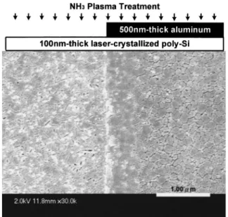
Additionally, Secco etching was also used to delineate grain boundaries with and without passivation. As shown in Fig. 3, a 100 nm thick laser-crystallized poly-Si film was
selectively treated with NH3plasma using aluminum patterns as hard masks, the insertion of which is schematically de-picted above Fig. 3. The aluminum patterns were then selec-tively removed using wet etchant. The grain boundaries in the aluminum cap region were clearly seen after Secco etch-ing. However, the grain boundaries near the aluminum-capped edge were ambiguous because they were passivated by hydrogen lateral diffusion,16thereby reducing the etching rate around the grain boundaries. This result implies that lateral diffusion of hydrogen may lead to a lack of uniformity in the passivation of grain boundaries throughout the channel region. Therefore, irregular I – V characteristics, such as hump effects, are evident in the subthreshold region.
B.I – V characteristics
Figures 4 and 5 show the transfer characteristics of a single TFT-A and the forward and reverse modes of a single TFT-B before and after NH3plasma treatment. A comparison
between TFT-A and TFT-B reveals that the decrease in the number of grain boundaries of the channel regions is accom-panied by a reduction in the threshold voltage and an in-crease in the field-effect mobility. This is because the grain boundaries trap electrons when gate voltage VGS is applied,
and generate surrounding depletion regions and lead to the formation of potential barriers. Meanwhile, strained bonds and dangling bonds at the grain boundaries generate band tail
FIG. 3. SEM photograph of an excimer laser-crystallized poly-Si film with and without NH3 plasma treatment after Secco etching. A 100 nm thick laser-crystallized poly-Si film was selectively treated with NH3plasma us-ing aluminum patterns as hard masks, shown schematically at the top.
FIG. 4. Transfer characteristics of TFT-A measured before and after NH3
plasma treatment for 2 h.
FIG. 5. Transfer characteristics of a single TFT-B measured in forward and reverse modes before and after NH3plasma treatment for 4 h.
states and deep level states in the band gap, respectively. These states can trap electrons, and reduce the ON current and increase the OFF current. However, the states can be passivated during NH3 plasma treatment,
17
and that would yield a steeper subthreshold slope for the hydrogenated TFT than that for the nonhydrogenated TFT. The ON/OFF current ratios and the field-effect mobility improve simultaneously after the grain boundaries are passivated. It should be noted that the leakage current of nonhydrogenated TFT-B at VDS
⫽12 V in reverse mode is significantly higher than that in
forward mode, as shown in Fig. 5. The increase in leakage current results from the marked increase in the number of grain-boundary trap states in the drain junction. Many carri-ers released by thermionic-field emission from the trap sites cause the leakage current in reverse mode to exceed that in forward mode.18,19 The leakage current is a function of the trap density in the drain junction, which was formulated by Olasupo and Hatalis18 and Fossum et al.20 Besides, the ON currents in both modes are almost identical because TFT-B is operated in the linear region. Figure 5 also indicates that measured threshold voltage Vth at VDS⫽12 V is 7.91 V in
forward mode and 6.60 V in reverse mode. The fall in Vthin
reverse mode results from an avalanche-induced short chan-nel effect.21 Electrons trapped at the grain boundaries en-hance the drain depletion length, essentially shortening the channel length at high drain bias. Furthermore, the transfer characteristics of TFT-B in both modes become symmetric following NH3 plasma treatment for 4 h because the grain
boundaries are effectively passivated, thus reducing the dif-ference between the numbers of trap states in the drain junc-tions in both modes.
The effects of grain boundaries in the drain junction on the performance of devices can be further elucidated from output characteristics of a single TFT-B in both modes and by comparing variation of Vth of devices of TFT-A and
TFT-B with the drain voltage. As shown in Fig. 6, the kink effect of nonhydrogenated TFT-B at VGS⫽20 V in reverse
mode appears to be stronger than that in forward mode. This phenomenon can be attributed to the drain-induced grain-boundary barrier lowering effect,22,23and the grain-boundary trap-induced avalanche generation effect.11The former effect is caused by drain bias VDS modulating the grain-boundary
potential barrier heights in the drain junction and forming asymmetric barriers. Extra carriers, which are injected from the lower side of the barriers into the side of the drain junc-tion, increase the drain current as the drain bias increases. The latter effect results from the high local electric fields created by charge states at grain boundaries of the drain junc-tion. The impact ionization process generates electron-hole pairs, resulting in the absence of saturation in the output characteristics.24Rates of carrier ionization, often expressed as an exponential function of the electric field, depend strongly on the electric field of the drain junction.25 Section III C, in which hot-carrier reliability is discussed, further elu-cidates this phenomenon. Besides, the drain currents in both modes are close to each other and significantly increase after NH3 plasma treatment for 4 h. The grain-boundary barrier
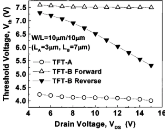
heights are lowered and more electrons are induced to be-come conduction carriers. Figure 7 shows a comparison of the variation of Vthwith the drain bias in TFT-A with that in
TFT-B. As VDS is varied from 5 to 15 V, Vth of TFT-A and
forward mode of the TFT-B remain almost unchanged, but Vth in reverse mode of TFT-B decreases as VDS increases.
This implies that VGSmust be reduced to maintain a constant
drain current as VDS increases, because grain boundaries
themselves create space charge regions that enhance local electric fields in the drain junction. Vth evaluated above VDS⫽5 V depends strongly on the location of the grain boundary. However, Vth at low drain bias, like VDS⫽0.1 V, depends strongly on the number of grain boundaries in the channel region, rather than on the grain-boundary locations. Trapping of charge at the grain boundaries also influences the drain depletion length when gate and drain voltages are applied.
C. Characterization of hot-carrier reliability
When excimer laser-crystallized poly-Si TFTs, with and without NH3 plasma treatment, are under static hot-carrier
stress, the behavior of these devices is degraded. The degra-dation can be characterized by the creation of trap states and the injection of hot carriers into the gate oxide. Figure 8 shows variations of the threshold voltage and the maximum transconductance of nonhydrogenated TFT-A and nonhydro-genated TFT-B associated with static hot-carrier stress for
FIG. 6. Output characteristics of a single TFT-B measured in forward and
reverse modes before and after NH3plasma treatment for 4 h. FIG. 7. Variations of threshold voltage Vthwith drain bias VDSfor
nonhy-drogenated TFT-A and nonhynonhy-drogenated TFT-B in both modes.
5791
J. Appl. Phys., Vol. 95, No. 10, 15 May 2004 Chen, Yeh, and Lou
104s. In particular, the single TFT-B was first stressed in forward mode for 104s and then stressed in reverse mode for 104s. TFT-A and TFT-B in forward mode are robust to hot-carrier stress, but the same stress strongly degrades the per-formance of TFT-B in reverse mode. Hence the hot-carrier reliability of the laser-crystallized poly-Si TFTs depends strongly on the locations of grain boundaries, rather than on the number of grain boundaries in the channel region. Mean-while, the number of grain boundaries of the drain junction is critical to the hot-carrier reliability of the devices. While TFT-B undergoes reverse stress for 104s, avalanche
multi-plication occurs through impact ionization in the drain junc-tion, generating many electron-hole pairs from the initially broken weak Si–Si bonds at grain boundaries of the drain junction and the more recently broken strong Si–Si bonds in the drain junction.26 The hot carriers induced damage at the grain boundaries of the drain junction, equivalent to intro-ducing serial resistance into the current path, thus reintro-ducing the ON currents, as evidenced by the serious degradation of TFT-B in reverse mode, as shown in Fig. 8. However, the ON currents of the devices with large grains in the drain junction, following the same stress for 104s, are either slightly increased or almost unchanged with respect to the initial ON currents. Figure 9 shows the transfer characteris-tics of forward mode of another TFT-B treated with the same
stress for 104s. Meanwhile, drain avalanche hot holes are
injected into the gate oxide by positive voltage VDG⫽10 V, slightly reducing Vthand slightly increasing the ON current, as clearly shown in the inset in Fig. 9. The hot holes screen damage at the grain boundaries of the drain junction, and this was also observed by stressing another TFT-B in reverse mode.
The hot-carrier reliability of devices with grain bound-aries in the drain junction is further investigated using an-other single TFT-B, which was first stressed in reverse mode for 104s and then directly stressed in forward mode for 102s. It should be noted that forward stress for 102s does not significantly damage TFT-B because the drain junction contains large grains in forward mode. The behavior of TFT-B in reverse mode was characterized continuously after the last 102s forward stress. As shown in the inset in Fig. 10, Vth at VDS⫽0.1 V increases with the stress time, but Vth at
VDS⫽5 V decreases as the stress time increases. This implies
that the hot holes injected into the gate oxide and the trap states created at the grain boundaries of the drain junction screen each other as gate voltage VGSis swept from low to
high at constant drain voltage of VDS⫽5 V. After stress is
applied for 104s, the subthreshold region in which the chan-nel exhibits weak inversion undergoes a parallel shift to lower VGS, because the hot holes injected into the gate oxide
shorten the channel. The hot holes in the gate oxide can be neutralized by attracting channel electrons during the for-ward stress applied for 102s.27 After the hot holes are
re-leased from the gate oxide, the subthreshold region shifts significantly toward higher VGS, as shown in Fig. 10. This implies that a large number of deep states are generated at the grain boundaries of the drain junction after the first re-verse stress has been applied for 104s. However, the drain currents at large VGS always decline as the stress time
in-creases because acceptor-like states created at the grain boundaries of the drain junction are introduced into the chan-nel and exhibit deep inversion. A comparison between OFF currents reveals donor-like states, as it does the acceptor-like states located near midgap. When negative VGS is applied, FIG. 8. Degradation of both the threshold voltage and the maximum
trans-conductance of nonhydrogenated devices with the stress time. ⌬Vth and
⌬Gm max/Gm max,iwere evaluated at VDS⫽0.1 V for the each stress time. The
single TFT-B was first stressed in forward mode and then stressed in reverse mode.
FIG. 9. Transfer characteristics of nonhydrogenated TFT-B measured in forward mode before and after forward stress was applied for 104s. The
inset presents a linear scale to show ON currents.
FIG. 10. Transfer characteristics of nonhydrogenated TFT-B measured in reverse mode before and after reverse stress was applied for 104s. The
curve associated with the neutralization of hot holes was plotted after the hot holes were released from the gate oxide by final forward stress applied for 102s. The inset plots⌬V
thwith the stress time at VDS⫽0.1 and 5 V,
respec-tively.
the OFF current of the neutralization of hot holes increases more slowly than the initial OFF current at VDS⫽5 V, as shown in Fig. 10. The donor-like states are positively charged when negative VGS is applied, so the electric field becomes weaker in the drain depletion region. This effect causes the OFF current that flows after stress has been ap-plied for 104s to be less than the initial OFF current at VGS⬍⫺25 V. This phenomenon is consistent with the results
obtained by Brown and Migliorato.28
NH3 plasma treatment can destroy the excellent
hot-carrier reliability of devices with large grains in the drain junction. Figure 11 shows variations of ⌬Vth and
⌬Gm max/Gm max,i with the stress time for devices that have
been hydrogenated. One can see that hot-carrier reliability of hydrogenated TFT-B in reverse mode is effectively pro-moted. The high local electric fields created at grain bound-aries of the drain junction can be effectively reduced because atomic hydrogen ties up the dangling and strained bonds during hydrogenation, thus reducing the number of carriers trapped at the grain boundaries. The Si–H bonds of the shal-low tail states are easily bound and are easily broken because they have small binding energy.17 Therefore, the behavior associated with degradation of devices differs from that of nonhydrogenated devices. Figure 11 exhibits the tendency to degrade. The degradation of devices after hydrogenation be-comes independent of the original distribution of the grain boundaries in the channel region. Figure 12 shows the trans-fer characteristics in reverse mode of another hydrogenated TFT-B following stress for 104s. In fact, the hydrogenated
devices of TFT-A and TFT-B after being stressed exhibit increased OFF currents, decreased ON currents, and reduced subthreshold slopes. The mechanism for device degradation involves the breaking of many Si–H bonds, which creates the shallow tail states in the upper half of the band gap. Additionally, the hump effect appears in the subthreshold region, especially after the channel region is asymmetrically damaged by hot-carrier stress, as shown in Fig. 12. This is also consistent with observations of hydrogenated TFT-A and hydrogenated TFT-B in forward mode. The hump effect originates in the nonuniformity of the passivation of grain boundaries throughout the channel region. The center of the
channel region has different turn-on characteristics from the two sides of the region because the lateral diffusion of hy-drogen activates trap states.
IV. CONCLUSION
In this study we reported the effects of grain boundaries on the performance and hot-carrier reliability of the laser-crystallized poly-Si TFTs with and without hydrogenation. The hot-carrier reliability of the devices strongly depends on the location of grain boundaries rather than on the number of grain boundaries of the channel region. Grain boundaries in the drain junction increase the leakage current, cause the threshold voltage to decline as the drain bias increases; en-hance the kink effect in output characteristics, and strongly degrade device performance under static hot-carrier stress. These effects are attributed to the generation of high local electric fields from surface roughness and trapping of charge at grain boundaries in the drain junction. NH3 plasma
treat-ment can effectively passivate grain boundaries that are ran-domly distributed in the channel region. However, hydroge-nation introduces the hump effect into the subthreshold region, and causes a trade-off between the electrical charac-teristics and the hot-carrier reliability of laser-crystallized poly-Si TFTs.
ACKNOWLEDGMENTS
The authors would like to thank the National Science Council, Taiwan, Republic of China, for financially support-ing this research under Contract No. NSC92-2215-E-009-025, and the Nano Facility Center共NFC兲 of National Chiao-Tung University and the National Nano Device Laboratory
共NDL兲 of the National Science Council for providing
equip-ment.
1S. S. Han et al., Digest of Technical Papers of 2003 SID共Society for Information Display, San Jose, CA, 2003兲, p. 208.
2C. H. Kim, I. H. Song, S. H. Jung, and M. K. Han, IEDM Technical Digest 共IEEE, Piscataway, NJ, 2001兲, p. 751.
3I. W. Wu, A. G. Lewis, T. Y. Huang, and A. Chiang, IEEE Electron Device Lett. 10, 123共1989兲.
FIG. 11. Degradation of both the threshold voltage and the maximum trans-conductance of hydrogenated devices with the stress time. These devices were treated with NH3plasma for 4 h, and⌬Vthand⌬Gm max/Gm max,iwere evaluated at VDS⫽0.1 V for each stress time. Two devices of TFT-B were
stressed in forward and reverse modes, respectively.
FIG. 12. Transfer characteristics of hydrogenated TFT-B measured in re-verse mode before and after the rere-verse stress was applied for 104s. The
device was treated using NH3plasma for 4 h. The hump effect in the
sub-threshold region is observed before and after hot-carrier stress is applied.
5793
J. Appl. Phys., Vol. 95, No. 10, 15 May 2004 Chen, Yeh, and Lou
12
H. C. Cheng, F. S. Wang, and C. Y. Huang, IEEE Trans. Electron Devices
44, 64共1997兲.
13J. S. Im and H. J. Kim, Appl. Phys. Lett. 64, 2303共1994兲.
14C. W. Lin, L. J. Cheng, Y. L. Lu, Y. S. Lee, and H. C. Cheng, IEEE Electron Device Lett. 22, 269共2001兲.
15
D. K. Fork, G. B. Anderson, J. B. Boyce, R. I. Johnson, and P. Mei, Appl. Phys. Lett. 68, 2138共1996兲.
25
S. M. Sze, Physics of Semiconductor Devices, 2nd ed.共Wiley, New York, 1981兲, Chap. 1.
26K. M. Chang, Y. H. Chung, G. M. Lin, C. G. Deng, and J. H. Lin, IEEE Electron Device Lett. 22, 475共2001兲.
27
B. S. Doyle, M. Bourcerie, C. Bergonzoni, R. Benecchi, A. Bravis, K. R. Mistry, and A. Boudou, IEEE Trans. Electron Devices 37, 1869共1990兲. 28T. M. Brown and P. Migliorato, Appl. Phys. Lett. 76, 1024共2000兲.