Electrical and dielectric behavior of MgO doped Ba 0.7 Sr 0.3 TiO 3 thin films on Al 2 O
3 substrate
S. Y. Lee and T. Y. Tseng
Citation: Applied Physics Letters 80, 1797 (2002); doi: 10.1063/1.1458067 View online: http://dx.doi.org/10.1063/1.1458067
View Table of Contents: http://scitation.aip.org/content/aip/journal/apl/80/10?ver=pdfcov
Published by the AIP Publishing
Articles you may be interested in
Impact of Morphological Features on the Dielectric Breakdown at SiO 2 /3 C SiC Interfaces
AIP Conf. Proc. 1292, 47 (2010); 10.1063/1.3518308
Optical and electrical properties of amorphous Gd x Ga 0.4x O 0.6 films in Gd x Ga 0.4x O 0.6 / Ga 2 O 3 gate dielectric stacks on GaAs
Appl. Phys. Lett. 84, 2521 (2004); 10.1063/1.1695445
Electrical properties of chemical-solution-derived Bi 3.54 Nd 0.46 Ti 3 O 12 ferroelectric thin films
J. Appl. Phys. 94, 7376 (2003); 10.1063/1.1622777
Structural and electrical characteristics of the interfacial layer of ultrathin ZrO 2 films on partially strain compensated Si 0.69 Ge 0.3 C 0.01 layers
J. Vac. Sci. Technol. A 21, 1758 (2003); 10.1116/1.1603279
Nonlinear electrical behavior of the TiO 2 WO 3 varistor
J. Appl. Phys. 92, 4779 (2002); 10.1063/1.1503853
This article is copyrighted as indicated in the article. Reuse of AIP content is subject to the terms at: http://scitation.aip.org/termsconditions. Downloaded to IP: 140.113.38.11 On: Thu, 01 May 2014 06:24:42
Electrical and dielectric behavior of MgO doped Ba
0.7Sr
0.3TiO
3thin films on
Al
2O
3substrate
S. Y. Lee, and T. Y. Tsenga)
Department of Electronics Engineering and Institute of Electronics, National Chiao-Tung University, Hsinchu 300, Taiwan, Republic of China
共Received 4 September 2001; accepted for publication 3 January 2002兲
In this letter, we present the results of the fabrication and characterization of 5 mol % MgO doped Ba0.7Sr0.3TiO3 共BST兲 films grown on Pt/TiN/SiO2 coated on Al2O3 substrates using the rf
magnetron sputtering technique. The dielectric and electrical properties of Ba0.7Sr0.3TiO3 thin film
were found to improve obviously by means of MgO doping. The leakage current density of BST thin film decreased about 1 order of magnitude on MgO doping, while BST film with MgO doping had a higher dielectric constant than that without MgO doping. The dielectric constant of the films increased with increasing annealing temperature due to the consistent increase in grain size and crystallinity. The 750 °C annealed, 100 nm thick film indicated a high dielectric constant of 440 at 100 kHz and the lattice constant of 3.986 Å. The improvement of the electrical properties of BST films was associated with the reduced oxygen vacancies due to improved oxygenation of BST films in the presence of MgO. The MgO doped BST films exhibited a high tunability of 25% and dc resistivity of 6⫻1010⍀ cm at an applied electric field of 200 kV/cm. The time-dependent dielectric
breakdown studies indicated that the films had a longer lifetime of over 10 yrs on operation at the electric field of 0.4 MV/cm which is better than undoped BST film. © 2002 American Institute of
Physics. 关DOI: 10.1063/1.1458067兴
The advancement of dynamic random access memories
共DRAMs兲 has significantly decreased the available area per
cell. Electroceramic thin films with high dielectric constant have attracted great attention for practical use in a capacitor of giga-bit DRAMs since the adoption of high dielectric con-stant materials can lower the height of the storage node and simplify the cell structure.1,2One of the most promising ma-terials for the capacitor dielectric film is (Ba1⫺xSrx)TiO3 共BST兲 because of its high dielectric constant, low leakage
current density, high dielectric breakdown strength, relatively low dielectric relaxation time, low temperature coefficient of dielectric constant, the composition dependent Curie tem-perature, and paraelectric perovskite phase that does not ex-hibit fatigue, aging, and the ease of composition control due to the absence of volatile lead oxide.3
According to previous investigations, the electrical and dielectric properties and reliability of BST films heavily de-pend upon the thin film deposition method, composition, dopant, postannealed temperature, base electrode, micro-structure, film thickness, surface roughness, oxygen content, and homogeneity of the film.4 – 6 Oxygen content in BST films has been identified to play an important role in deter-mining the electrical and dielectric behavior of BST film. Inadequate oxygenation of BST films during growth in low oxygen partial pressure at elevated temperature may lead to the formation of oxygen vacancies, which act as charged traps. These charged traps leading to increased electron con-centration affect the properties of BST film detrimentally.7A suitable dopant can be used to decrease the concentration of electrons. In this letter, we report the improvement in
elec-trical properties of BST films by means of MgO doping. The dielectric constant, dielectric loss, and leakage current den-sity of MgO doped BST films annealed at various tempera-tures were characterized with respect to measurement param-eters such as applied electric field and measurement temperature. Experimental results indicate that the leakage current density of the BST film with 5 mol % MgO doping can be improved about 1 order of magnitude, while the di-electric constant of MgO doped film is 30% higher than that of undoped film.
In this letter, the undoped and 5 mol % MgO doped BST (Ba/Sr⫽70/30) targets with a diameter of 2 in. and thickness of 1/4 in. were prepared using a standard solid-state powder-mixing reaction process. The sputtering chamber was evacu-ated to a base pressure of 2⫻10⫺6Torr. All films were pre-pared at a fixed power of 100 W共the power density is 2.26 W/cm2兲 and constant pressure of 40 mTorr, which was main-tained by a mixture of argon and oxygen at a mixing ratio of 1:1 with a total flow of 20 sccm. All BST films have the same thickness of around 100 nm. The substrate temperature was at 500 °C. The purpose of deposition of SiO2 on the
Al2O3 substrate was to improve surface roughness of the
Al2O3 surface. The TiN layer was deposited between Pt and
SiO2/Al2O3 to enhance the interface adhesion and provide a
diffusion barrier.
The grain size and film morphology analysis of the films were carried out by using atomic force microscopy 共Digital Instruments Nano-Scope III兲 to reveal a simple dependence of grain growth on annealing temperature ranging from 550 to 750 °C in O2 for 30 min in a rapid-thermal-annealing 共RTA兲 furnace. The 50 nm thick Pt top electrode with a
di-ameter of 250 m was then formed by sputtering and pat-terned by the shadow mask process. The film thickness was
a兲Author to whom correspondence should be addressed; electronic mail:
APPLIED PHYSICS LETTERS VOLUME 80, NUMBER 10 11 MARCH 2002
1797
0003-6951/2002/80(10)/1797/3/$19.00 © 2002 American Institute of Physics
This article is copyrighted as indicated in the article. Reuse of AIP content is subject to the terms at: http://scitation.aip.org/termsconditions. Downloaded to IP: 140.113.38.11 On: Thu, 01 May 2014 06:24:42
determined from ellipsometry. The microstructural features of the films were examined by x-ray diffraction共XRD兲 共Si-emens D5000兲. The dielectric and electrical measurements were conducted on the films in the metal–insulator–metal capacitor configuration. The leakage current of Ba0.7Sr0.3TiO3films was measured with a voltage step of 0.1 V and elapsed time of 30 s. The capacitance was measured at 100 kHz as a function of voltage from positive to negative bias. Dielectric constant of the films was calculated from the capacitance measured at 100 kHz without bias voltage. The dielectric properties were measured as a function of fre-quency with a HP 4194A impedance/gain phase analyzer. The insulating properties were evaluated from current– voltage and current–time measurements by measuring the current through the sample using HP 4156. The Pt top elec-trode of the BST capacitor was connected to the voltage source and the bottom electrode was ground.
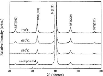
Figure 1 shows the XRD patterns of the 50% OMR BST thin films doped with 5 mol % MgO deposited on Pt bottom electrodes at substrate temperature 500 °C and postannealed for 30 min at 550, 650, and 750 °C in O2 ambient. The
pur-pose of using 50% OMR is that the BST films with large grain size can exhibit large dielectric constants due to polar-ization of electric dipoles on the basis of a previous study.8 The oxygen stoichiometry also influences the dielectric con-stant of the films. The 共110兲 peak intensity of the BST thin films becomes more intense in the XRD patterns with in-creasing temperature from 550 to 750 °C in O2 ambient. It indicates from Fig. 1 that the crystallinity of those films is improved after the RTA process.
Figure 2 shows the variation of dielectric constant of both undoped and 5 mol % MgO doped BST thin films with RTA temperature. It depicts that the dielectric constant of MgO doped BST film is higher than that of undoped BST film at various RTA temperatures. The dielectric constant is related to oxygen stoichiometry, grain size, and crystallinity of the film. The average grain sizes of 5 mol % MgO doped as-deposited and 750 °C annealed BST films determined by Scherrer’s formula are 417 and 493 Å, respectively, com-pared to undoped BST film, which are 378 and 436 Å under the same conditions. Therefore, the increase in dielectric constant may be attributed to the grain growth and improved
crystallinity of the films on the basis of the XRD result. From our experimental result, the dielectric constant and dis-sipation factor of the BST films are 390 and 0.004, respec-tively, while those of undoped BST films are 345 and 0.012, respectively, under being postannealed at 650 °C in an O2
ambient. The better dielectric properties observed in MgO doped BST films are attributed to better crystallization, denser structure, and larger grain size compared to undoped BST film.
The root mean square surface roughnesses of MgO doped and undoped BST films increase with increasing an-nealing temperatures ranging from 550 to 750 °C共not shown here兲. The increasing surface roughness may be due to grain growth of annealed BST films. It can confirm this from the XRD data共Fig. 1兲 that the grain size increases with increas-ing annealincreas-ing temperature. The MgO-doped films have higher surface roughnesses compared to undoped films, which is attributed to better crystallization and larger grain size of MgO doped films.
The difference in the leakage current characteristics of undoped and MgO-doped BST films is shown in Fig. 3. It is indicated that the leakage current density of MgO-doped BST film is about 1 order of magnitude lower than that of undoped BST films. Consider the addition of MgO into BST films. On the basis of the similarity in ionic radii between Mg2⫹ (reff⫽0.72 Å) and Ti4⫹ (reff⫽0.61 Å) in sixfold
FIG. 1. XRD patterns of 5 mol % MgO doped BST films annealed in O2for
30 min at temperatures indicated.
FIG. 2. Plots of dielectric constant vs annealing temperature for 5 mol % MgO doped and undoped BST film.
FIG. 3. Plots of leakage current density vs electric field for 5 mol % MgO doped and undoped BST film annealed at temperatures indicated.
1798 Appl. Phys. Lett., Vol. 80, No. 10, 11 March 2002 S. Y. Lee and T. Y. Tseng
This article is copyrighted as indicated in the article. Reuse of AIP content is subject to the terms at: http://scitation.aip.org/termsconditions. Downloaded to IP: 140.113.38.11 On: Thu, 01 May 2014 06:24:42
coordination,9it may be assumed that Mg replaces Ti in the BST lattice and a doubly ionized oxygen vacancy is simul-taneously formed, i.e.,
MgO共 – TiO2兲→MgTi
⬙
⫹Vo••⫹OoX, 共1兲where Vo•• is an extrinsic oxygen vacancy controlled by the Mg content. Mg behaves as an electron acceptor-type dopant, which can prevent reduction of Ti4⫹to Ti3⫹by neutralizing the donor action of the oxygen vacancies. In high tempera-ture deposition of BST films under nonoxidizing atmosphere, such as Ar, generally produces oxygen vacancies in the film according to
Oo→Vo••⫹2e
⬘
⫹1/2O2共g兲, 共2兲where Oo, Vo••, and e
⬘
represent the oxygen ion on itsnor-mal site, oxygen vacancy, and electron, respectively. From Eqs. 共1兲 and 共2兲, it can be seen that both MgTi
⬙
and Vo•• are compensated for each other because they play the role of an acceptor and a donor in BST film, respectively. Oxygen va-cancies created with MgO addition combined with the equi-librium reaction 共2兲 requires that the concentration of elec-tron be simultaneously decreased.This decrease in electron concentration leads to lower leakage current of MgO doped BST film compared to un-doped BST film. In Fig. 2, it is also indicated that 5 mol % MgO doped BST film has relatively low loss tangent com-pared to undoped BST film, which is consistent with the result of the lower leakage current of MgO-doped films shown in Fig. 3. The leakage current characteristics are dis-tinctly similar in the positive and negative voltage region. The symmetry in positive and negative voltage parts of the
J – E characteristic is due to the identical top and bottom
electrode work functions in the two interfaces. It also implies that the leakage current is electrode limited.10,11 It is gener-ally known that the leakage current of Pt/BST/Pt is con-trolled by Schottky barriers at the top BST/electrode and bottom BST/electrode interfaces. However, if these potential barriers are identical, then the J – E characteristics would be symmetric.
The leakage current density of the 550 °C annealed films is lower than those of 650 and 750 °C annealed films. The leakage current of BST film increases with increasing an-nealing temperature, which may be due to the enhanced ionic polarization and improved crystallinity with larger grain size. However, this enhanced ionic polarization would increase the energy dissipation during the relaxation,12,13 and films with large grain size also have short conduction paths along the highly resistive grain boundary, which cause an increase in the leakage current. This phenomenon implies that the higher dielectric constant and leakage current exhibited in the films annealed at temperatures above 550 °C may be at-tributed to their larger grain sizes. In our experiment, the leakage current density of MgO-doped BST film annealed at 650 °C for 30 min was 2⫻10⫺10A/cm2 at 100 kV/cm.
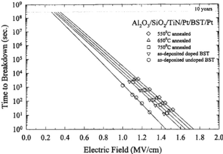
Figure 4 shows the lifetime extrapolation from depen-dence of cumulative failure on time-dependent dielectric breakdown 共TDDB兲 stress time for the 100 nm thick films annealed at different temperatures. The TDDB studies indi-cate that all the films have a lifetime of over 10 yrs of
op-eration at an electric field of 0.4 MV/cm. From Fig. 4, MgO doped BST films have a longer lifetime than undoped BST. The lifetime decreases with increasing annealing tempera-ture.
In conclusion, our investigation demonstrated that MgO can be an effective dopant for increasing the dielectric con-stant, reducing the leakage current, and enhancing the reli-ability of Ba0.7Sr0.3TiO3 thin films. We have shown that
550 °C annealed MgO doped BST film has a dielectric con-stant of 372, a loss tangent of 0.0037 at 100 kHz, a leakage current of 1⫻10⫺10A/cm2at an electric field of 100 kV/cm, and a delay time 30 s, while 550 °C annealed undoped film has 329, 0.011, and 1⫻10⫺8A/cm2, respectively. Present studies suggest that the improved dielectric and insulating properties of MgO-doped BST films are suitable for tunable microwave and integrated capacitor applications.
The authors gratefully appreciate financial support from the National Science Council of the Republic of China under Project No. NSC 90-2212-E-009-029 and Cyntec Co., Ltd, Hsinchu, Taiwan.
1T. Horikawa, N. Mikami, T. Makita, J. Tanimura, M. Kataoka, K. Sato,
and M. Nunoshita, Jpn. J. Appl. Phys., Part 1 32, 4126共1993兲.
2
S. Ezhilvalavan and T. Y. Tseng, Mater. Chem. Phys. 65, 227共2000兲.
3M. Yamamuka, T. Kawahara, T. Makita, A. Yuuki, and K. Ono, Jpn. J.
Appl. Phys., Part 1 35, 729共1996兲.
4C. S. Hwang, S. O. Park, H. J. Cho, C. S. Kang, H. K. Kang, S. I. Lee, and
M. Y. Lee, Appl. Phys. Lett. 67, 2819共1995兲.
5
M. S. Tsai and T. Y. Tseng, IEEE Trans. CPMT 23, 128共2000兲.
6Y. F. Kuo and T. Y. Tseng, Electrochem. Solid-State Lett. 2, 236共1996兲. 7T. S. Chen, V. Balu, B. Jiang, S. H. Kuah, J. C. Lee, P. Chu, R. E. Jones,
P. Zurcher, D. J. Taylor, and S. Gillespie, Integr. Ferroelectr. 16, 191
共1997兲.
8M. S. Tsai, S. C. Sun, and T. Y. Tseng, J. Appl. Phys. 82, 3482共1997兲. 9H. H. Wang, F. Chen, S. Y. Dai, T. Zhao, H. B. Lu, D. F. Cui, Y. L. Zhou,
Z. H. Chen, and G. Z. Yang, Appl. Phys. Lett. 78, 1676共2001兲.
10
S. Yamamichi, P. Y. Lesaicherre, H. Yamaguchi, K. Takemura, S. Sone, H. Yabuta, K. Sato, T. Tamura, K. Nakajima, S. Ohnishi, K. Tokashiki, Y. Hayashi, Y. Kato, Y. Miyasaka, M. Yoshida, and H. Ono, IEEE Trans. Electron Devices 44, 1076共1997兲.
11K. Abe and S. Komatsu, J. Appl. Phys. 77, 6461共1995兲. 12
J. Gerblinger and H. Meixner, J. Appl. Phys. 67, 7453共1990兲.
13M. Yoshida, H. Yamaguchi, T. Sakuma, and Y. Miyasaka, J. Electrochem.
Soc. 142, 244共1995兲.
FIG. 4. TDDB lifetime as a function of electric field for 5 mol. % MgO doped films annealed at temperatures indicated and as-deposited undoped BST film.
1799
Appl. Phys. Lett., Vol. 80, No. 10, 11 March 2002 S. Y. Lee and T. Y. Tseng
This article is copyrighted as indicated in the article. Reuse of AIP content is subject to the terms at: http://scitation.aip.org/termsconditions. Downloaded to IP: 140.113.38.11 On: Thu, 01 May 2014 06:24:42