Letter
Large-area non-close-packed nanosphere deposition by blade coating
for vertical space-charge-limited transistor
Yen-Chu Chao
a, Kai-Ruei Wang
b, Hsin-Fei Meng
a,⇑, Hsiao-Wen Zan
b,⇑, Yung-Hsuan Hsu
aaInstitute of Physics, National Chiao Tung University, Taiwan
bDepartment of Photonics and Institute of Electro-Optical Engineering, National Chiao Tung University, Taiwan
a r t i c l e
i n f o
Article history: Received 7 June 2012
Received in revised form 9 September 2012 Accepted 14 September 2012
Available online 10 October 2012 Keywords: Blade coating Colloidal lithography Vertical channel Polymer transistor
a b s t r a c t
In this work, we proposed a fast and controllable blade coating process to form close-packed nanosphere structures. We investigated the key to obtain well-distributed non-close-packed PS spheres with blade coating. We utilized the blade-coated nanosphere structure to realize colloidal lithography and fabricate a vertical channel polymer transis-tor, the space-charge-limited transistor (SCLT). We demonstrated that SCLT utilizing blade-coated nanospheres delivered 13.9 mA/cm2at 1.8 V with an on/off current ratio as 45,000.
The process of blade-coating nanospheres may facilitate the commercialization of low-cost colloidal lithography.
Ó 2012 Elsevier B.V. All rights reserved.
1. Introduction
Polystyrene (PS) spheres with well-defined diameters are common nanostructure templates. PS spheres can form 2D or 3D close-packed structures that are used commonly as photonic crystals [1]. Non-close-packed nanosphere structures are also used in numerous novel solid-state tronic devices, such as solid-state sensors with porous elec-trode surfaces [2], vertical channel space-charge-limited transistors (SCLTs) [3,4], and high mobility indium-gallium-zinc oxide thin-film transistors with dot-like doping [5]. These devices possess superior performance qualities when non-close-packed nanosphere structures are employed. However, current processes for forming non-close-packed nanosphere structures are unable to be commercialized. For example, ordered non-close-packed PS spheres are formed by reducing the diameter of close-packed PS spheres using reactive-ion etching techniques [6]. Forming close-packed PS spheres is a time-consuming process (e.g., 7 h for 1 cm2close-packed spheres). Previous
studies, including our own previous work, have used a dipping process to form disordered non-close-packed PS spheres[3,4,7]. Although it is a rapid process, it has poor reproducibility because it depends significantly on human factors.
This study proposes a fast and controllable blade-coat-ing process to form non-close-packed nanosphere struc-tures. This study examines key concepts for obtaining well-distributed non-close-packed PS spheres using blade coating. Finally, this paper shows that a vertical channel space-charge-limited transistor (SCLT) using blade-coated non-close-packed PS spheres delivers a current density of 13.9 mA/cm2 at 1.8 V with an on/off current ratio of
45,000.
Fig. 1a shows a polymer SCLT, which is a 3-terminal de-vice that functions similar to a vacuum tube triode. The carrier holes are injected into the semiconducting polymer using an emitter, passing through the openings at the base, and are finally collected by the collector. The magnitude of the potential barrier constructed between the emitter and the collector at the vertical channel controls the SCLT on/ off states[3,4].
The ideal metal grid in SCLTs has a high density of sep-arated holes. Therefore, PS spheres require a high density
1566-1199/$ - see front matter Ó 2012 Elsevier B.V. All rights reserved.
http://dx.doi.org/10.1016/j.orgel.2012.09.013
⇑Corresponding authors.
E-mail addresses:[email protected](H.-F. Meng),hsiaowen@ mail.nctu.edu.tw(H.-W. Zan).
Contents lists available atSciVerse ScienceDirect
Organic Electronics
and sparse distribution when used as a shadow mask for Al-based evaporation.
PS sphere aggregates cause large holes in the metal grid. Consequently, a significant transistor off-current occurs be-cause the current passing through these holes cannot be controlled by the surrounding metal potential[8].
Commer-cial PS spheres are a colloidal suspension in ethanol, and their surfaces are electrically charged in the ethanol solu-tion. They recombine with counter ions in ethanol and be-come neutralized when ethanol evaporates. PS spheres are deposited using a dipping method during transistor fabrica-tion. The dipping method can only be applied to small areas
Fig. 1. (a) The schematic diagram and (b) the fabrication process of P3HT SCLT.
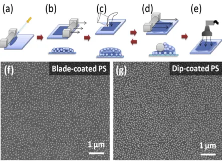
Fig. 2. The process involved in the blade method. (a) Drop the ethanol solution of PS spheres. (b) PS spheres are deposited on the substrate. (c) Boiling IPA is poured over the substrate. (d) Pushing the other spheres away. (e) Drying the remaining IPA. (f) SEM image of 100 nm blade-coated PS spheres. (g) SEM image of 100 nm dip-coated PS spheres.
and depends significantly on human factors. Therefore, this method is unsuitable for future mass production.
2. Experimental
Fig. 1b shows the SCLT fabrication process. The SCLT was fabricated on an indium tin oxide (ITO) glass substrate that is plasma cleaned and smoothed with 100 W O2
plas-ma for 10 min. A 200 nm layer of crosslinkable polyvinyl-pyrrolidone (PVP) is spin-coated onto the ITO substrate, and then cross-linked at 200 °C for 60 min in an inert atmosphere. Methylated poly(melamine-co-formalde-hyde) is used as the cross-linking agent. The PVP is then coated with a 20 nm poly(3-hexylthiophene) (P3HT) layer and annealed at 200 °C for 10 min. Xylene is used to spin-rinse the P3HT to remove the soluble sections. The remaining P3HT has an estimated thickness of 15 nm.
PS spheres suspended in ethanol are first deposited on the substrate using a cylindrical blade (Fig. 2a and b), which is separated from the substrate by a 30
l
m gap. An ethanol layer (with suspended spheres) with thicknessaround the gap size is formed. Numerous PS spheres are adsorbed onto the substrate to form a monolayer while ex-cess PS spheres are still suspended in the ethanol layer. To remove the excess spheres, boiling isopropyl alcohol (IPA) is poured onto the wet substrate (Fig. 2c) to produce a large aqueous volume with suspended spheres. Then, a 120
l
m gap blade is used to quickly sweep the substrate to remove most of the IPA with suspended spheres (i.e. the blade-cleaning process shown in Fig. 2d). The cycle of pouring boiling IPA and the blade-cleaning process, named as the IPA rinse process, is repeated 3–4 times to remove all spheres that have not been adsorbed. Finally, as shown in Fig. 2e, a hair dryer is used to dry the remaining IPA quickly. The PS ethanol solution concentration is fixed at 0.4 wt.% for the initial deposition by blade coating. Lower concentrations produce insufficient PS sphere densities. The blade gap is 30l
m for the initial deposition and 120l
m for the IPA rinse process.A 40-nm-thick layer of Al is then deposited onto the PVP layer to form the metal base electrode. The PS spheres are removed using adhesive tape and the PVP at sites
out Al coverage are removed using O2plasma treatment at
100 W for 10 min. The PVP is then functionalized with an octadecyltrichlorosilane (OTS) self-assembly monolayer (SAM). A 350 nm P3HT layer is spin-coated onto the sub-strate using a 4.5 wt.% chlorobenzene solution. Finally, the MoO3/Al collector is deposited to complete the SCLT
with active area as 1 mm2or 1 cm2. 3. Results and discussions
The distribution of PS spheres deposited by blade coat-ing with multiple boilcoat-ing IPA rinse process (Fig. 2f) is almost as effective as the dip coating deposition process (Fig. 2g), despite producing slightly more aggregates.
As discussed the critical step during the PS sphere blade-coating is the repeated IPA rinse following the initial depo-sition of the PS spheres by blade coating in the ethanol solu-tion. The IPA rinse process reduces the PS sphere aggregates. The boiling IPA redissolves the PS spheres, and the IPA is quickly removed by the blade, followed by blow drying. During this process, the aggregated PS spheres become electrically charged and move freely in accordance with
the Coulomb’s Law. This process can be repeated many times to reduce the aggregates. Blow drying is performed at room temperature because high temperatures melt the PS spheres (not shown).Fig. 3shows the number of aggre-gates in a specific area for the distributions with various flush times. The distribution is poor when the IPA rinse is not performed (Fig. 3a) or when it is performed only once (Fig. 3b). The aggregates are reduced significantly after the second rinse (Fig. 3c), and there is a slight improvement when the process is repeated 4 times (Fig. 3e). The distribu-tion displayed inFig. 3d is sufficient for SCLT fabrication, as shown below.
Compared with the dip coating method, the advantage of blade coating PS spheres is that large and uniform distri-butions can be obtained easily. Scanning electron micros-copy (SEM) is used to examine several positions in the 1 cm2area (Fig. 3j).Fig. 3g–i shows similar distributions of average PS sphere density and aggregate level. Specifi-cally, the average PS sphere densities in Fig. 3g–i are 17.8, 20.0, and 19.6 numbers per
l
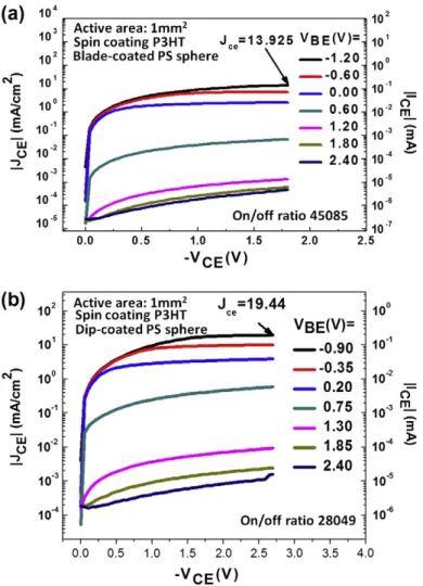
m2. A 10% variation is obtained. Such uniformity cannot be achieved using the dip coating method. The blade-coated sphere densityvari-Fig. 4. The output characteristics for P3HT SCLT fabricated with (a) blade-coated PS spheres and (b) dip-coated PS spheres. The current density and the total output current are labeled by the left y-axis and right y-axis, respectively.
ation is due to the disturbance of IPA flushing process. In this experiment, IPA flushing is realized by pouring boiling IPA directly on blade-coated PS sphere region. In future work, the disturbance of IPA flushing may be avoided by smoothly flowing IPA through the blade-coated PS sphere region. Furthermore, it is anticipated that this process can be scaled up to 10 cm if a larger blade is used. There-fore, blade coating is shown to be suitable for cost-efficient mass production of nanogrid structures over large areas.
This study now focuses on SCLTs with an Al base fab-ricated using PS spheres deposited by blade coating. First, the results for a small active area of 1 mm2are discussed,
and transistors with 1 cm2 active areas are shown later.
All the discussed devices use P3HT as channel material and the PVP is functionalized with an OTS SAM. For SCLT fabricated with blade-coated PS spheres, a collector cur-rent density (Jc) as a function of collector voltage (VCE)
is shown in Fig. 4a. The output current density Jc is
approximately 13.9 mA/cm2 when V
CE= 1.8 V and the
on/off current ratio is approximately 45,000. Fig. 1a shows the device structure. The transistor is in top-emis-sion mode when the holes are injected from the top MoO3/Al emitter into the P3HT valence band and
subse-quently collected by the bottom ITO collector. Fig. 4b shows the transistor characteristic for SCLTs fabricated using conventional dip-coated PS spheres under identical
conditions. The collector on-current is approximately 17.9 mA/cm2when V
CE= 1.8 V and the on/off current ratio
is approximately 28,000. These results are similar to those of devices that are fabricated using blade-coated PS spheres.
Therefore, this verifies the feasibility of using blade-coated PS spheres to fabricate vertical polymer SCLTs. The cost efficiency and high current output of SCLTs with blade-coated PS sphere technology are also shown. To crease the output current, the SCLT active region is in-creased to 1 cm2. To reduce the production cost, the expensive ITO electrode is replaced by a dual-layer Al/ MoO3electrode. To improve the DC bias endurance ability,
the PVP and P3HT thickness are increased to 400 and 550 nm, respectively. The device structure and the Jc–VCE
characteristics of such a large-area low-cost SCLT are shown inFig. 5a and b, respectively. The output current density is 2.5 mA/cm2when V
CE= 1.8 V, and the on/off
cur-rent ratio is approximately 2400. Compared to the device performance shown inFig. 4a, the slightly reduced output current density and on/off current ratio in Fig. 5b are potentially caused by the increased channel length (i.e., P3HT thickness) and the minor oxidation of the bottom Al electrode during oxygen plasma etching. However, the total output current of the large-area SCLT is as high as 2.5 mA. This high output current generated from a
low-Fig. 5. (a) The schematic diagram of a large-area low-cost SCLT without using an ITO electrode. (b) The output characteristics for the large-area low-cost SCLT.
cost organic transistor facilitates the development of cost-efficient power devices. Specifically, the proposed colloidal lithography with blade-coated PS spheres does not require expensive conventional lithography processes and is com-patible with roll-to-roll processing. We anticipate that the process can be scaled up to 10 cm by using a larger blade. Therefore, blade coating is shown to be suitable for the cost-efficient mass production of SCLTs with nano-grid structures over large areas.
4. Conclusion
This study successfully showed a colloidal lithography process using a blade-coating deposition process. A solution with PS spheres is deposited onto the substrate by blade coating. Excess PS spheres are removed by rinsing with boil-ing IPA followed by blade coatboil-ing. A non-close-packed PS sphere structure with uniform distribution is obtained by controlling the initial PS sphere density and the frequency of IPA rinsing. The proposed blade-coated PS spheres were then used to fabricate a vertical channel polymer SCLT. This study showed that SCLTs fabricated with blade-coated PS spheres and those fabricated with conventional dip-coated PS spheres possess similar characteristics. Furthermore, this paper showed that a large-area cost-efficient SCLT delivers a total output current as high as 2.5 mA, thereby facilitating
the development of cost-efficient organic power devices. We anticipate that the proposed colloidal lithography formed by blade-coated PS spheres can be scaled up to an area approximately 100 cm2
by increasing the blade size. This study provides a potential foundation for achieving cost-efficient colloidal lithography in real production environments.
Acknowledgements
This work is supported by the National Science Council of Taiwan (100-2628-M-009-002).
References
[1] B.V. Lotsch, G.A. Ozin, J. Am. Chem. Soc. 130 (2008) 15252–15253. [2] H.J. In, C.R. Field, P.E. Pehrsson, Nanotechnology 22 (2011) 355501. [3] Y.C. Chao, C.H. Chung, H.W. Zan, H.F. Meng, M.C. Ku, Appl. Phys. Lett.
99 (2011) 233308.
[4] Y.C. Chao, M.C. Ku, W.W. Tsai, H.W. Zan, H.F. Meng, H.K. Tsai, S.F. Horng, Appl. Phys. Lett. 97 (2010) 223307.
[5] H.W. Zan, W.W. Tsai, C.H. Chen, C.C. Tsai, Adv. Mater. 23 (2011) 4207. [6] K.Y. Wu, Y.T. Tao, C.C. Ho, W.L. Lee, T.P. Perng, Appl. Phy. Lett. 99
(2011) 093306.
[7] K. Fujimoto, T. Hiroi, K. Kudo, M. Nakamura, eJ. Surf. Sci. Nanotechnol. 3 (2005) 327–331.
[8] Y.C. Chao, M.C. Niu, H.W. Zan, H.F. Meng, M.C. Ku, Org. Electron. 12 (2011) 78.