Geometrical correlations of quantum dots in InAs/GaAs superlattice structure from
electron tomography
Y. H. Wu, L. Chang, L. C. Chen, H. S. Chen, and F. R. Chen
Citation: Applied Physics Letters 93, 153108 (2008); doi: 10.1063/1.2998693
View online: http://dx.doi.org/10.1063/1.2998693
View Table of Contents: http://scitation.aip.org/content/aip/journal/apl/93/15?ver=pdfcov Published by the AIP Publishing
Articles you may be interested in
Site-controlled formation of InAs/GaAs quantum-dot-in-nanowires for single photon emitters Appl. Phys. Lett. 100, 263101 (2012); 10.1063/1.4731208
Influence of wetting layers and quantum dot size distribution on intermediate band formation in InAs/GaAs superlattices
J. Appl. Phys. 110, 073105 (2011); 10.1063/1.3631785
Characterization of excitonic features in self-assembled InAs/GaAs quantum dot superlattice structures via surface photovoltage spectroscopy
J. Appl. Phys. 101, 103102 (2007); 10.1063/1.2733992
Mechanisms of lateral ordering of InAs/GaAs quantum dot superlattices J. Vac. Sci. Technol. B 21, 1920 (2003); 10.1116/1.1588645
Structural characterization of InAs/GaAs quantum-dot nanostructures Appl. Phys. Lett. 78, 4133 (2001); 10.1063/1.1382855
This article is copyrighted as indicated in the article. Reuse of AIP content is subject to the terms at: http://scitation.aip.org/termsconditions. Downloaded to IP: 140.113.38.11 On: Wed, 30 Apr 2014 22:52:18
Geometrical correlations of quantum dots in InAs/GaAs superlattice
structure from electron tomography
Y. H. Wu,1,a兲 L. Chang,1L. C. Chen,2H. S. Chen,3and F. R. Chen3
1Department of Materials Science and Engineering, National Chiao-Tung University, Hsinchu 300, Taiwan 2Process Failure Analysis Department, Taiwan Semiconductor Manufacturing Company Ltd.,
Science-Based Industrial Park, Hsinchu 300, Taiwan
3Department of Engineering and System Science, National Tsing-Hua University, Hsinchu 300, Taiwan
共Received 7 May 2008; accepted 22 September 2008; published online 14 October 2008兲
In this study, the three-dimensional共3D兲 information about the structural properties of quantum dots 共QDs兲 in InAs/GaAs superlattice structure has been illustrated using electron tomography in the mode of high-angle angular dark-field scanning transmission electron microscopy. Comparison of this 3D reconstruction with the two-dimensional projection at the same positions is made. The structural properties of embedded quantum dots have been evaluated from electron tomography. The correlation relationship of QDs in superlattice structure has been understood by accurate measurements of 3D geometric positions, which can be free of the overlapping effect from 2D cross section along different crystallographic orientations. © 2008 American Institute of Physics. 关DOI:10.1063/1.2998693兴
Self-assembled semiconductor quantum dots 共QDs兲 formed by the Stranski–Krastanow growth mode due to lat-tice mismatch are valuable nanostructures because of their outstanding electronic and optical properties, especially for laser applications.1,2 Varying depositing conditions of QDs may modify the structural properties due to the strain field around QDs, such as size, shape, and density, that strongly influence electronic structure of nanostructures and the band gap.3 However, luminescence intensity of QDs in a single layer cannot meet the requirement for laser applications. For practical usage, semiconductor QDs are normally grown in superlattice structures in order to improve the luminescence yield, so characteristic arrangements of QDs could be re-sulted from the interaction between vertical and lateral strain fields among different layers.4–6The periodic features in the superlattice quantum structure depending on the spacer thickness may have either correlated or anticorrelated ar-rangement. The phenomena had been reported in the hetero-structure superlattice systems such as InAs/GaAs, InAs/InP, PbSe/PbEuTe, CdSe/ZnSe, and SiGe/Si.7–10Scanning tunnel-ing microscopy共STM兲 and transmission electron microscopy 共TEM兲 in cross section are often the main tools to character-ize the structural properties of embedded QDs, which only reveal two-dimensional共2D兲 information.11,12TEM observa-tions of correlated QDs in superlattice structures using pro-jected data may not easily uncover the real structure due to the overlapping effect in 2D, as a result of lacking third dimension information. In addition, for conventional TEM in bright-field and dark-field images, the strain-induced diffrac-tion contrast may shed the QDs in a 100–200 nm thick TEM specimen. High-resolution transmission electron microscopy 共HRTEM兲 observations of some characteristic properties of QDs such as size and shape are a difficult task because a thin sample of thickness less than 20–40 nm for requirements of HRTEM may lack sufficient number of QDs. Incomplete STM data in the depth direction may show uncertainty for buried QDs as well.
TEM electron tomography has been well established for three-dimensional 共3D兲 characterization of biological and amorphous materials.13,14Although the electron tomography using bright-field TEM and energy-filtered TEM can be achieved in principle for crystalline materials, they may not be easy to obtain the acceptable 3D information because of the diffraction contrast effect, limitation of specimen thick-ness, and poor signal-to-noise ratio.15 Electron tomography reconstructed from a tilt series of high-angle angular dark-field scanning transmission electron microscopy 共HAADF-STEM兲 images is a promising technique for the investigation of crystalline materials in 3D.16 The contrast in HAADF-STEM images is approximately proportional to Z1.7共Z is the
atomic number of the scattering atom兲, which can be inter-preted in terms of the relative element ratio directly.17Arslan et al.18used the HAADF-STEM imaging technique to dem-onstrate electron tomography for nanocrystals and Ge/Si QDs. More recently, Inoue et al.19 demonstrated HAADF-STEM electron tomography for a single embedded InAs QD in GaAs. The only study of tomography of QD superlattice has been recently done by Müller et al.20 using 3D atom probe technique. Here, we investigated 3D geometrical cor-relations of capped QDs in InAs/GaAs superlattice structure using electron tomography based on HAADF-STEM mode from which 3D crystallographic information can be ex-tracted.
The self-assembled QDs superlattice structure on GaAs 共001兲 substrates consisted of 30 periods of InAs 共2.62 mono-layers兲 and GaAs spacer layer 共30 nm兲, which were grown by molecular beam epitaxy at 485 and 600 ° C, respectively. For 关010兴 cross-sectional TEM specimen preparation, me-chanical grinding and polishing were used to thin a specimen to about 500 nm thickness, followed by Ar+milling at 4 kV with a low incident angle. The 5 nm colloidal gold particles in acetone were dropped uniformly onto a TEM specimen as fiducial markers for accurate alignment of acquisition of a tilt series of HAADF-STEM images and for reconstruction. In this study, electron tomography was performed in a FEI Tec-nai F20 microscope with a high-tilt single-axis sample holder. STEM-HAADF images were acquired on a Fischione a兲Electronic mail: [email protected].
APPLIED PHYSICS LETTERS 93, 153108共2008兲
0003-6951/2008/93共15兲/153108/3/$23.00 93, 153108-1 © 2008 American Institute of Physics
This article is copyrighted as indicated in the article. Reuse of AIP content is subject to the terms at: http://scitation.aip.org/termsconditions. Downloaded to IP: 140.113.38.11 On: Wed, 30 Apr 2014 22:52:18
Model 3000 annular dark field detector with an inner collec-tion angle about 70 mrad at a magnificacollec-tion of 225 000⫻ using a 1 nm probe. The FEI XPlore 3D tomography suite was used to control the operation of image acquisition in a wide range of tilt angle from −70° to +70° in 1° increments with the tilt axis along 关001兴GaAs to minimize the missing
wedge effect. After complete alignment of TEM, automatic operation of recentering and refocusing STEM-HAADF im-ages of gold particles by the phase-correlation method was adopted during this tilting process.21 The weighted back-projected algorithm used for reconstruction of tomography data from the 141 tilt-series images was performed with the FEI program. The GaAs spacer layer thickness in such a superlattice structure can be used for z-axis scale calibration. The successfully reconstructed data did display a rotational movie smoothly without any jumpiness. Furthermore, the wedge shape of the TEM specimen was faithfully exhibited in reconstructed tomography.
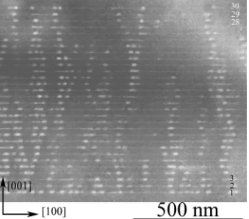
Figure 1 shows a HAADF image of the whole QD su-perlattice structure taken along GaAs关010兴 direction at low magnification. The bright regions are indium-rich and corre-spond to the wetting layers and QDs. It is seen the 30 periods of alternating InAs QDs and wetting layers with 30 nm GaAs spacer. The wetting layer as a set of white parallel lines is about 1 nm thick with the indium concentration of x⬃0.12 in InxGa1−xAs as determined from the Z-contrast values
rela-tive to the GaAs ones. Observations of vertical arrangement of InAs QDs in this projected image show that the QDs are distributed in an angular range of 65° – 85° with respect to the wetting layer surface, indicating that the QDs may not be vertically aligned.
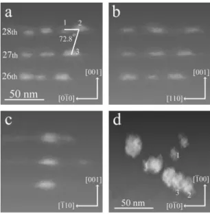
The tomographic reconstruction in Fig.2共a兲of a 3D per-spective view shows the distribution of 72 QDs within the top eight layers of the whole structure in a rectangular parallel-piped volume of 133⫻524⫻240 nm3. The inset in
Fig.2共a兲shows two of the QDs in the 27th layer after vol-ume rendering. For quantitative analysis of the superlattice structure, sliced images and segmentation of a reconstructed volume were used to examine the shape, the size, and distri-bution of the QDs. Typical sliced images from three adjacent layers 共28th to 26th兲 are illustrated in Fig. 2共b兲. From the reconstruction, the shape of the buried QDs can be recog-nized as lenslike, and the size of the QDs within the eight layers is estimated to be around 18–25 nm in width as mea-sured along关100兴 and 关010兴 and about 7 nm above the wet-ting layers in height in the growth direction of关001兴. It can
also be shown that the size of the QDs is not uniformly distributed. The density of QDs in each layer is determined from the sliced images of the total eight layers共not shown兲. Since the volume contains only 72 QDs in this tomography data set, it may not give good statistics with accuracy. There is about 14% difference in the density of QDs in the same volume between the values determined from the 3D recon-struction and from the 2D projections due to the overlapping effect. The difference may increase significantly in the cases of a high QD density structure and a thicker TEM specimen with increased possibility of the overlap.
Figure3共a兲is a histogram from 45 pairs of QDs within the reconstructed volume, showing the distances of the first nearest neighbor共the 1st NN兲 of QDs in adjacent layers. The FIG. 1. Cross-sectional HAADF-STEM image showing QDs InAs/GaAs
superlattice structure in关010兴.
FIG. 2. 共a兲 Volume rendering of reconstruction showing the distribution of InAs QDs within the top eight layers. The bright contrast obtained after removing GaAs background corresponds to indium-containing regions. The inset showing two of the QDs.共b兲 Typical sliced images from three adjacent layers共layers 28–26兲.
FIG. 3. 共a兲 Histogram of the nearest neighboring distance between QDs in the adjacent layers. 共b兲 Histogram of the nearest neighboring distance be-tween QDs in the same layer.
153108-2 Wu et al. Appl. Phys. Lett. 93, 153108共2008兲
This article is copyrighted as indicated in the article. Reuse of AIP content is subject to the terms at: http://scitation.aip.org/termsconditions. Downloaded to IP: 140.113.38.11 On: Wed, 30 Apr 2014 22:52:18
distances of the 1st NN measured from center to base-center of neighboring QDs are important for quantification of geometric correlations. Most of the distances are 32.5 nm, which is slightly larger than the periodic GaAs spacer thick-ness in 30 nm. This result suggests that the strain caused by the underlying QDs may laterally displace the lateral posi-tions of subsequently formed QDs. Lateral shift of a depos-ited dot with respect to a buried one in an underlying layer is about 8.8 nm along 具110典 and the vertically deviated angle from 关001兴 is about 15°. The histogram in Fig. 3共b兲 illus-trates the distribution of the distance of the 1st NN of 23 pairs QDs in the same layer to show 2D arrangement of QDs, and most of the distances appear to be about 17.5 nm, which is equal to two times lateral shift in the adjacent layers.
Figure 4共a兲is a projected view of a local volume 关the same region to show the sliced images in Fig. 2共b兲兴 along 关100兴. The included angle between lines 12 and 23 among the three dots denoted as 1, 2, and 3 in Fig. 4共a兲 of a 2D projection image is 72.8°. However, the real angle in 3D between these three QDs as measured from the sliced images of these two layers from the reconstructed tomography data is actually 82°. Detailed analysis of the QDs in the eight layers shows that the characteristic 3D angle is 80⫾5°.
Furthermore, electron tomography provides observations of a crystalline specimen along various orientations. The projected images of the same QDs distributed in 3D can be visualized along 关100兴, 关11¯0兴, 关110兴, and 关001兴 crystallo-graphic orientations as shown in Figs. 4共a兲–4共d兲, respec-tively. Due to the relatively thick specimen and the tilting limit of the sample holder, it is almost impossible to observe structural properties of capped QDs in conventional TEM in such a wide range of projection directions. TEM evidence of GaAs-based nanostructures along 关110兴 direction has been presented in many studies because of relatively easy speci-men preparation and observation, but the symmetric proper-ties of QDs may be sometimes lost from the data in a single crystallographic orientation. Projected images such as Figs.
4共a兲–4共c兲 may not realize the real situation that QDs are aligned approximately along⫾关11¯0兴 and ⫾关110兴 directions. From Figs.4共a兲and4共c兲, the measured width of QDs in the 关100兴 projected image is smaller than in the关110兴 one, imply-ing that the base of QDs may be not circular. If we observe the QDs from关001¯兴, the shape of quantum dots is nearly like a rectangle as shown in Fig.4共d兲, and the edges of the quan-tum dots are parallel to 具100典 in consistence with observa-tions of planar QDs arrays in InAs/GaAs system in other studies.19,22
In summary, the actual behavior of capped quantum dots in InAs/GaAs superlattice structure with 30 nm thick GaAs spacer has been successfully revealed using electron tomog-raphy with the HAADF-STEM technique. The reconstruc-tion shows that the shape of embedded InAs QDs is lenslike. Most of the embedded QDs in 3D distribution form a char-acteristic arrangement in the adjacent layers with lateral shift of 8.8 nm in 具110典 relative to the underlying QDs and an included angle of 80° among three neighboring QDs in ad-jacent layers.
The authors thank Taiwan Semiconductor Manufacturing Co. 共TSMC兲 for supporting this research and providing the
tomography facilities and Y. F. Kao for the help on STEM operation. The QD samples were provided by R. S. Hsiao of Industrial Technology Research Institute, Hsinchu, Taiwan.
1V. A. Shchukin and D. Bimberg,Rev. Mod. Phys. 71, 1125共1999兲. 2V. M. Ustinov and A. E. Zhukov, Semicond. Sci. Technol. 15, R41
共2000兲.
3M. Grundmann, O. Stier, and D. Bimberg,Phys. Rev. B52, 11969共1995兲. 4A. E. Zhukov, A. R. Kovsh, N. A. Maleev, S. S. Mikhrin, V. M. Ustinov, A. F. Tsatsul’nikov, M. V. Maximov, B. V. Volovik, D. A. Bedarev, Yu. M. Shernyakov, P. S. Kop’ev, Zh. I. Alferov, N. N. Ledentsov, and D. Bim-berg,Appl. Phys. Lett. 75, 1926共1999兲.
5V. A. Shchukin, D. Bimberg, V. G. Malyshkin, and N. N. Ledentsov,Phys. Rev. B 57, 12262共1998兲.
6X. D. Wang, N. Liu, C. K. Shih, S. Govindaraju, and A. L. Holmes, Jr., Appl. Phys. Lett. 85, 1356共2004兲.
7Q. Xie, A. Madhukar, P. Chen, and N. P. Kobayashi,Phys. Rev. Lett. 75, 2542共1995兲.
8G. Springholz, V. Holy, M. Pinczolits, and G. Bauer, Science 282, 734 共1998兲.
9G. Springholz, M. Pinczolits, P. Mayer, V. Holy, G. Bauer, H. H. Kang, and L. Salamanca-Riba,Phys. Rev. Lett. 84, 4669共2000兲.
10V. Holy, G. Springholz, M. Pinczolits, and G. Bauer,Phys. Rev. Lett. 83, 356共1999兲.
11L. Ouattara, J. M. Ulloa, A. Mikkelsen, E. Lundgren, P. M. Koenraad, M. Borgstrom, L. Samuelson, and W. Seifert, Nanotechnology 18, 145403 共2007兲.
12M. Gutierrez, M. Herrera, D. Gonzalez, R. Garcia, and M. Hopkinson, Appl. Phys. Lett. 88, 193118共2006兲.
13A. J. Koster, R. Grimm, D. Typke, R. Hegerl, A. Stoschek, J. Walz, and W. Baumeister,J. Struct. Biol. 120, 276共1997兲.
14R. C. N. Melo, A. M. Dvorak, and P. F. Weller, Microscopy and Analysis 21, 15共2007兲.
15H. Friedrich, M. R. McCartney, and P. R. Buseck,Ultramicroscopy 106, 18共2005兲.
16P. A. Midgley and M. Weyland,Ultramicroscopy 96, 413共2003兲. 17S. Hillyard and J. Silcox,Ultramicroscopy 58, 6共1995兲.
18I. Arslan, T. J. V. Yates, N. D. Browning, and P. A. Midgley,Science 309, 2195共2005兲.
19T. Inoue, T. Kita, O. Wada, M. Konno, T. Yaguchi, and T. Kamino,Appl. Phys. Lett. 92, 031902共2008兲.
20M. Müller, A. Cerezo, G. D. W. Smith, L. Chang, and S. S. A. Gerstl, Appl. Phys. Lett. 92, 233115共2008兲.
21J. S. Tsai, J. J. Kai, L. Chang, and F. R. Chen,J. Electron Microsc. 53, 371 共2004兲.
22A. Nakamura, A. N. Titkov, M. Ichida, V. P. Evtikhiev, and K. Kryga-novskii Appl. Phys. A: Mater. Sci. Process. 66, S1035共1998兲.
FIG. 4. Projections of QDs within a local volume from 26–28th layers along 共a兲 关100兴, 共b兲 关11¯0兴, 共c兲 关110兴, and 共d兲 关001兴 zone axes showing the relative geometric positions of InAs QDs in the adjacent layers.
153108-3 Wu et al. Appl. Phys. Lett. 93, 153108共2008兲
This article is copyrighted as indicated in the article. Reuse of AIP content is subject to the terms at: http://scitation.aip.org/termsconditions. Downloaded to IP: 140.113.38.11 On: Wed, 30 Apr 2014 22:52:18