國 立 交 通 大 學
電子工程學系電子研究所
博 士 論 文
應用於生醫感測與高速網路之
互補式金氧半光偵測器
CMOS Photodetectors for Biomedical Detections
and High-Speed Networks
研 究 生 :張育維
指導教授 :黃遠東博士
應用於生醫感測與高速網路之
互補式金氧半光偵測器
CMOS Photodetectors for Biomedical Detections
and High-Speed Networks
研 究 生:張育維
Student: Yu-Wei Chang
指導教授:黃遠東博士
Advisor: Dr. Yang-Tung Huang
國 立 交 通 大 學
電 子 工 程 學 系 電 子 研 究 所
博 士 論 文
A Dissertation
Submitted to Department of Electronics Engineering and Institute of Electronics College of Electrical and Computer Engineering
National Chiao Tung University in Partial Fulfillment of the Requirements
for the Degree of Doctor of Philosophy
in
Electronic Engineering
July 2009
Hsinchu, Taiwan, Republic of China
應用於生醫感測與高速網路之
互補式金氧半光偵測器
研 究 生:張育維
指導教授:黃遠東博士
國 立 交 通 大 學
電子工程學系電子研究所
摘 要
本研究提出四種應用於生醫感測與高速網路之積體互補式金氧半(CMOS)光偵測 器,研究內容包含了設計、分析、製作、與量測。在生醫感測的應用上,提出PP + /N 指狀光二極體(finger photodiode)搭配轉阻放大電路(trans-impedance amplifier),可量測過氧 化氫(H O )、葡萄糖(glucose)與組織胺(histamine)的最低濃度分別為 1 μM、1 μM與 10 μM;提出基板浮接(floating bulk)環狀光電晶體(ring-shaped phototransistor)搭配外環光二
極體,在可見光波段具有高於1000 A/W的響應度(responsivity),對於辣根過氧化酶(HRP) 的檢測極限為 2.7 pM。在高速網路的應用上,提出的網狀空間調變光二極體(spatially modulated photodiode),可有效地把光電流中的慢速成分扣除,所設計製作的元件展現 出5.5 GHz的高頻寬;提出之具深N 層的PIN光二極體,其深N 層被連接到高電位以 排除在P 層所產生的慢速擴散載子,所設計製作的元件對於 50 Ω負載可達 800 mV 輸 出電壓與 2.5 Gbps操作速度。所開發之光偵測器效能皆比文獻上其他金氧半光偵測器 高。 well 2 2 well well sub pp
CMOS Photodetectors for Biomedical Detections
and High-Speed Networks
Student: Yu-Wei Chang
Advisor: Dr. Yang-Tung Huang
Department of Electronics Engineering and Institute of Electronics
National Chiao Tung University
ABSTRACT
The design, analysis, manufacture, and measurements of the four integrated CMOS photodetectors for biomedical detections and high-speed networks are presented. For biomedical applications, the proposed P+
/Nwell finger photodiode with a trans-impedance
amplifier demonstrated that the minimum concentration successfully detected for H2O2,
glucose, and histamine were 1 μM, 1 μM, and 10 μM, respectively; the proposed ring-shaped phototransistor with a floating bulk enclosed by a ring-shaped photodiode exhibited a responsivity higher than 1000 A/W for the visible spectrum range and a detection limit of 2.7 pM for HRP (horse-radish peroxidase). For high-speed applications, the meshed SMPD (spatially modulated photodiode) can effectively subtract the deferred portion from the immediate portion of the photocurrent, and the manufactured device demonstrated a high bandwidth of 5.5 GHz; the proposed DNW-based (deep-Nwell-based) PIN photodiode, in
which the slowly diffusive carriers generated in Psub are decoupled from the photocurrent by
connecting the DNW to a positive supply voltage, was capable of outputting 800 mVpp with
up to 2.5 Gbps for 50-Ω loads. These proposed photodetectors exhibited better performances than other reported CMOS photodetectors.
誌 謝
博班生涯看似短短幾年,實則對整個長遠的人生有著莫大助益。這段期間的歷練, 幫助我內心成長與蛻變,一一回想起來都相當珍貴,要感謝的人有好多好多。 首先,我想感謝指導教授黃遠東老師多年來的殷殷教誨,言教上,孜孜不倦地引導 我嚴謹踏實的求學態度,身教上,始終秉持著一絲不苟的處世原則。看到老師常常費盡 氣力地批改大大小小的研究論文,只希望學生能夠早點進入狀況獨當一面,我深深地體 會到蠟燭那種不惜燃燒自己只為照亮別人的精神,感動萬分。此外,老師也訓練我學習 採購儀器、建立系統、撰寫計畫、接待外賓、出國觀摩、擔任助教、帶專題生,並鼓勵 我參與服務學習、為原住民上山課輔,熱心公益、開闊人生觀,這些五彩繽紛的豐富經 驗,讓我覺得博班生涯不虛此行,值回票價! 對於跨領域的研究而言,想要把元件設計、生醫檢測、高速網路整合起來,單靠我 一根朽木是難撐大廈的,幸好有了許多志同道合的夥伴一起來築夢。在生醫檢測的應用 上,感謝楊裕雄老師的指導,以及夥伴游秉鈞、戴妤庭、林明瑜的協助。在高速網路的 應用上,感謝陳巍仁老師的指導,以及夥伴劉川漳、黃世豪的協助。關於論文內容的呈 現,也感謝各位口試委員所給予的肯定與寶貴建議。 實驗室的成員能夠齊聚一堂,就是一種緣分。感謝博班學長鄧俊修、許世欣、許俊 彥、裴廷漢、林俊廷、呂明峰的經驗分享,以及博班同儕楊玉麟、徐新峰、陳建華的相 互照應,當然還有每年來來去去、族繁不及備載的碩班學弟所帶來的歡樂氣氛。 在精神層面上,我很感謝爸爸、媽媽、弟弟、女友這一路上的支持與鼓勵,心的力 量是無遠弗屆、沒有極限的!遇到任何境界,只要正面積極地看待,都可以轉化為生生 增上的泉源。在此也由衷地感謝上 日下 常老和尚慈悲的甘露法語,以及福智團體所提供的 學習資源,幫助我更瞭解生命的價值,建立崇高的人生目標。站在巨人的肩膀上,讓我 可以看得更高、更遠、更美好。所以,只要是對一切眾生無限生命有幫助的事,不論過 程有多艱辛、別人都不願意作的,我也要努力去完成它! 祝福大家,都能獲得最圓滿的快樂 ^_^Contents
Contents iv
List of Tables vii
List of Figures viii
1 Introduction 1
1.1 Integrated CMOS Photodetectors . . . 1
1.2 Integrated CMOS Photodetectors for Biomedical Applications . . . 2
1.3 Integrated CMOS Photodetectors for High-Speed Applications . . . 3
1.4 Organization of The Dissertation . . . 4
2 Optoelectronic Integrated Circuits for Biomedical Applications 5 2.1 Introduction . . . 5
2.2 Principles and Methods . . . 5
2.2.1 Absorption Photometry . . . 5
2.2.2 Biochemical Reactions . . . 6
2.2.3 Finger Photodiode and Transimpedance Ampli…er . . . 7
2.2.4 Biosensing System Setup . . . 11
2.2.5 Preparation of Biochemical Reagents . . . 12
2.3 Experimental Results . . . 12
2.3.1 Characteristics of the Whole System . . . 12
2.3.2 H2O2 Detection . . . 13
2.3.3 Glucose Detection . . . 17
2.3.4 Histamine Detection . . . 19
2.4 Summary . . . 20
3 Ring-Shaped Phototransistors for Biomedical Applications 23 3.1 Introduction . . . 23
3.2 Principles and Methods . . . 23
3.2.1 Absorption Photometry . . . 23
3.2.2 Biochemical Reaction . . . 24
3.2.3 Ring-Shaped Phototransistor . . . 25
3.2.4 Biosensing System Setup . . . 26
3.2.5 Preparation of Biochemical Reagents . . . 27
3.3 Experimental Results . . . 28
3.3.1 Device Characteristics . . . 28
3.3.2 HRP Detection . . . 30
3.4 Applications for Screening Skin-Whitening Agents . . . 32
3.4.1 Motivation . . . 32
3.4.2 Materials and Methods . . . 33
3.4.3 Experimental Results . . . 35
3.5 Applications for Ultra-Violet Detection . . . 38
3.5.1 Motivation . . . 38
3.5.2 Operating Principle . . . 39
3.5.3 Experimental Results . . . 41
3.6 Summary . . . 43
4 Spatially-Modulated Photodiodes for High-Speed Applications 45 4.1 Introduction . . . 45
4.2 Device Structure and Operation Mechanism . . . 45
4.3 Theoretical Analysis of the Photocurrent . . . 47
4.3.1 General Considerations . . . 47
4.3.2 Square-Shaped SMPD . . . 48
4.3.3 Meshed SMPD . . . 50
4.4 Simulations of the Photocurrent Response . . . 52
4.4.1 Simulation Parameters . . . 52
簡歷
生化名詞中英對照
Abbreviations
Appendix 87
4.4.3 N+/P
well or P+/Nwell Junctions with VR= 5 V . . . 58
4.4.4 In‡uence of Geometric Size . . . 59
4.4.5 Parasitic Capacitance . . . 60
4.5 Measurement Results . . . 60
4.6 Summary . . . 61
5 Deep-Nwell Based Photodiodes for High-Speed Applications 64 5.1 Introduction . . . 64
5.2 Principles and Methods . . . 65
5.2.1 Deep-Nwell Based PIN Photodiode . . . 65
5.2.2 Subsequent Circuits . . . 69
5.3 Experimental Results . . . 71
5.4 Summary . . . 75
6 Conclusion 76 6.1 Integrated CMOS Photodetectors for Biomedical Applications . . . 76
6.2 Integrated CMOS Photodetectors for High-Speed Applications . . . 77
6.3 Future Work . . . 78
Bibliography 80
117 115 113
List of Tables
3.1 The statistical information of the photocurrent response Iph and the
ab-sorbance A for VDS = 3 V and VGS = 2 V under various HRP
concen-tration. . . 32 3.2 The UV/blue responsivity of the CMOS photodetectors. . . 44 4.1 Doping concentrations and junction depths. . . 54 4.2 Characteristics of the photodetectors for Nwell/Psub, N+/Pwell, and P+/Nwell
List of Figures
2-1 The absorption spectrum of ABTS and ABTS+. . . . 7
2-2 The diagram of the miniature CMOS optical biosensing system and the experimental setup. . . 8 2-3 The top view and cross section of P+/N
well …nger photodiode. . . 9
2-4 The calculated re‡ectance as a function of wavelength for the device with and without passivation layers. . . 10 2-5 The con…guration of the subsequent circuit. Device parameters are M0 =
(100 m=0:5 m), M1 = M2 = (50 m=0:5 m), Mb0 = Mb1 = Mb2 = (1
m=0:5 m), R0 = 8 k , and Rb0 = 15 k . . . 11
2-6 Experimental results of the CMOS optical biosensing system with RF = 10
M and RF = 1 M at = 650 nm. (a) The output voltage versus the
input optical power. (b) The corresponding absorbance versus the output voltage. . . 14 2-7 Experimental results of the CMOS optical biosensing system with RF = 10
M and RF = 1 M at = 430 nm. (a) The output voltage versus the
input optical power. (b) The corresponding absorbance versus the output voltage. . . 15 2-8 Experimental results of the H2O2 detection with 650-nm light at 25 C.
(a) Real-time measurement of the output voltage for t = 0–80 s. (b) The Michaelis-Menten plot. . . 16 2-9 Experimental results of the H2O2 detection with 430-nm light at 37 C.
(a) Real-time measurement of the output voltage for t = 0–80 s. (b) The Michaelis-Menten plot. . . 17
2-10 Experimental results of the glucose detection with 650-nm light at 25 C. (a) Real-time measurement of the output voltage for t = 0–200 s. (b) The Michaelis-Menten plot. . . 18 2-11 Experimental results of the histamine detection with 430-nm light at 37
C. (a) Real-time measurement of the output voltage for t = 0–1200 s. (b) The Michaelis-Menten plot. . . 19 2-12 The absorbance A of the reaction mixture versus the AA concentration.
(a) At low concentration. (b) At high concentration. . . 21 3-1 The top view and cross section of the PMOS phototransistor. . . 25 3-2 The phototransistor-based biosensing system: (a) photogragh and (b)
il-lustrated diagram. . . 27 3-3 The measured I-V charateristics of the PMOS phototransistor. . . 28 3-4 The optoelectronic characteristics of the PMOS phototransistor for VDS =
3 V with various VGS: (a) photocurrent response versus illumination
intensities and (b) responsivity versus illumination intensities. . . 29 3-5 The photocurrent response versus HRP concentration for VDS = 3V with
various VGS. . . 30
3-6 The measured I-V characteristics for VGS = 0 V under various HRP
con-centrations. . . 31 3-7 The photocurrent response versus HRP concentration for VDS = 0:1 V
and VGS = 0 V. . . 32
3-8 The corresponding absorbance versus (a) photocurrent response and (b) HRP concentration. . . 33 3-9 The schematic diagram of three major assays for evaluating whitening agents. 34 3-10 The measured Id-Vd curves for the melanin assay. . . 36
3-11 The measured Id-Vd curves for the MTT assay. . . 37
3-12 The measured Id-Vd curves for the tyrosinase assay. . . 37
3-13 The e¤ects of Kojic acid on B16-F10 cells for melanin, MTT, and tyrosinase assays. . . 38 3-14 The top view, cross section, and equivalent symbol of the proposed (a)
3-15 The measured I-V characteristics of the PMOS phototransistor without
illumination. . . 41
3-16 The optoelectronic characteristics of the PMOS phototransistor for VDS = 3 V with various VGS: (a) photocurrent response versus illumination intensities and (b) DC responsivity versus illumination intensities. . . 42
4-1 The top view and cross section of (a) the Nwell/Psub square-shaped SMPD and (b) the Nwell/Psub meshed SMPD. . . 46
4-2 Connecting con…gurations of TIA and SMPD adopting (a) Nwell/Psub junc-tions or N+/P well junctions, and (b) P+/Nwell junctions. . . 53
4-3 Top views and cross sections of (a) …nger photodiode and (b) …nger-shaped SMPD. . . 54
4-4 Photocurrent response of the Nwell/Psub …nger photodiode with VR = 1 V. . 56
4-5 Photocurrent response of the Nwell/Psub …nger-shaped SMPD with VR = 1 V. . . 57
4-6 Photocurrent response of the Nwell/Psub square-shaped SMPD with VR = 1 V. . . 57
4-7 Photocurrent response of the Nwell/Psub meshed SMPD with VR = 1 V. . . 58
4-8 The relationship between the 3-dB bandwidth and WP of Nwell/PsubSMPDs with W = 2:1 m. . . 59
4-9 The experimental setup for the frequency response measurement. . . 61
4-10 The measured frequency response of the Nwell/Psub square-shaped SMPD. . 62
4-11 The measured frequency response of the Nwell/Psub meshed SMPD. . . 62
5-1 Top view and cross section of the PIN photodiode. . . 66
5-2 Hole density in the N+ di¤usion neutral region. . . 67
5-3 Simulated frequency response of PIN PD responsivity . . . 69
5-4 (a) VR = 6 V (b) VR = 2 V. . . 70
5-5 Monolithically integrated optical receiver architecture . . . 71
5-6 Chip micrograph . . . 72
5-7 Measured Bit error rate performance under (a) 2 V and (b) 6V. . . 73
5-8 Measured eye diagram performance (a) at 622 Mbps (under 2 V) and (b) at 2.5 Gbps (under 6 V). . . 74
6-1 The top view and cross section of the proposed SMPT to have a high gain and a high bandwidth. . . 79
Chapter 1
Introduction
1.1
Integrated CMOS Photodetectors
The CMOS (Complementary Metal-Oxide Semiconductor) technology is economi-cally the most important technology for the manufacture of microelectronic circuits [1]. Its power dissipation is much smaller than other technologies, and this allows to integrate much more CMOS gates on IC (integrated circuits) than in NMOS or bipolar technology, resulting in much better performance.
Semiconductors are the ideal material for internal photoelectric e¤ect because of the high carrier mobility, the low dark current, and the high e¢ ciency for carriers generation compared to phonon generation or single carrier excitation [2]. For a semiconductor photodetector, the electron-hole pairs generated by photon absorption contribute to the internal electrical conduction of the device, and contribute to a corresponding current at the contacts of the external circuits.
The realization of photodetectors in a standard CMOS technology has attracted much interest in the last decade. This is owing to its low cost, high throughput, and the ca-pability for integration with subsequent circuits without any process modi…cation. These properties enable the manufacture of complete data-acquisition systems on a single silicon chip [3].
For a integrated CMOS photodetector, there is a trade-o¤ between the gain and the bandwidth. The photodetector for biomedical applications is focused on the high gain, whereas the photodetector for high-speed applications is focused on the high bandwidth. In this dissertation, the design, analysis, manufacture, and measurements of the
pro-posed CMOS photodetectors for biomedical applications and high-speed applications are presented respectively.
1.2
Integrated CMOS Photodetectors for Biomedical
Applications
With the rapid progress of biotechnology and microelectronics, a new generation of biomedical diagnosis is expected worldwide. The development of a portable, accurate, inexpensive, and easy-to-use biosensor has become the most important niche in the health care industry [4], [5]. Detecting the optical properties changed by chemical reactions is a competent approach to examine various important biological molecules [6], [7].
Among the optical biosensing techniques, emission photometry and absorption pho-tometry have drawn substantial attention in the area of medical diagnosis [4]–[12]. Emis-sion photometry is the detection of the light emitted by molecules through chemical reactions in response to the concentration of an analyte. The light emission process can further be classi…ed into chemiluminescence, ‡uorescence, and phosphorescence according to speci…c characteristics. This popular technique is capable of real-time measurement with high selectivity to the analyte. However, it may su¤er from luminophor degenera-tion, which leads to signal attenuation with time [7]–[11]. Circumventing this di¢ culty, absorption photometry, another widely used technique, relies on the change of photon absorption through chemical reactions in response to the analyte concentration. The biosensing system based on absorption photometry o¤ers advantages for analyte monitor-ing with high spatial resolution and has potential for applications in microarray analysis [7], [12].
Regarding the commercial instruments for optical analysis, a photomultiplier tube usually serves as the optical sensor in a spectrophotometer. Commonly used wavelength range includes ultraviolet and visible light. Despite its high sensitivity, the spectropho-tometer has limited applications in home care instruments because of its bulky size, high cost, and high voltage (about 1000 V) [2]. On the other hand, the integrated CMOS photodetector is characterized as having a small size, a low cost, a high throughput, and low power consumption. Hence it becomes an attractive candidate for personalized diag-nostic kits. Although much research has been devoted to CMOS biosensor using emission
photometry, few studies have been done on CMOS biosensor using absorption photometry [7], [9].
In this research, two optical biosensing system were developed based on absorption photometry. The proposed integrated CMOS photodetectors include the …nger photo-diodes and ring-shaped phototransistors. Experimental results demonstrated high sensi-tivities, and the miniature systems would have potential toward a practical home care instrument for personalized clinical diagnosis.
1.3
Integrated CMOS Photodetectors for High-Speed
Applications
Due to the steadily increasing demands for system clock frequencies, electrical in-terconnects su¤er a lot from design problems, including system synchronization, power dissipation, impedance matching, and pin inductance. To avoid these problems, using optical interconnects between chips or boards would be an e¤ective way [13], [14]. The semiconductor materials suitable for optical components can be generally divided into two categories. On the one hand, optical components manufactured in III-V materials require a hybrid technology, which leads to a relatively high cost and high power consumption. On the other hand, silicon is characterized as high throughput and low cost, and hence becomes an attractive candidate for integrating photodetectors with subsequent circuits. In a standard CMOS technology, a P/N junction can be formed by adopting the Nwell/Psub, N+/Pwell, or P+/Nwell junction. For 850-nm incident light, the absorption
depth of silicon is approximately 16.7 m, and the Nwell/Psubjunction is typically adopted
to achieve a wider depletion region as well as a larger drift current. But the Nwell/Psub
junction depth (about 2 m) is so shallow that a large portion of photogenerated car-riers are deep in the substrate and results in a slow di¤usion response. Consequently, a traditional CMOS photodiode made by a single Nwell/Psub junction is not capable of
high-speed operation. E¤orts were contributed to circumvent this bottleneck in recent years, such as the …nger photodiode [15], [16] and the …nger-shaped spatially modulated photodiode (SMPD) [17]–[20]. The …nger photodiode adopts interdigitated P/N junctions to increase the depletion regions. It can improve the responsivity, but the photocurrent is still dominated by the substrate current, which makes the improvement in bandwidth
insigni…cant. The …nger-shaped SMPD composes of a row of junction diodes which are alternatively covered and uncovered with optical masks. This SMPD structure …nds a way to weaken the in‡uence of the substrate current by subtracting the deferred portion from the immediate portion of the photocurrent.
In this research, two types of CMOS photodetectors were investigated to further im-prove the frequency response: enhanced SMPDs and deep-Nwell based photodiodes.
Ex-perimental results exhibited higher operating speed compared to the prior art, and the proposed photodetectors would be bene…cial to the high-speed networks.
1.4
Organization of The Dissertation
This dissertation is organized as follows. Chapter 2 deals with a biosensing system on the basis of the …nger photodiode and trans-impedance ampli…er. The biomedical detections of H2O2, glucose, and histamine are also examined. Chapter 3 is concerned
with the ring-shaped phototransistor, which exhibits a high sensitivity and a low sample-volume requirement for the biomedical detection. In Chapter 4, the square-shaped SMPD and meshed SMPD are addressed to eliminate the slow substrate photocurrent for higher bandwidth. Chapter 5 presents the deep-Nwell based PIN photodiodes for applications in
high-speed networks. Finally, the conclusion is given and the future works are suggested in Chapter 6.
Chapter 2
Optoelectronic Integrated Circuits
for Biomedical Applications
2.1
Introduction
Based on a standard CMOS technology and absorption photometry, an optical biosens-ing system is proposed [21]. The whole system was assembled into a compact prototype, and it exhibits a high sensitivity and real-time measurement capability.
2.2
Principles and Methods
2.2.1
Absorption Photometry
The absorbance A of the materials is described by the Beer-Lambert law [6]
A = log I I0
= l c =) A _ c (2.1)
where I0 and I respectively denote the initial light intensity and the light intensity after
passing through the material, is the wavelength-dependent molar absorptivity in units of l mol 1 cm 1, l is the path length in units of cm, and c is the concentration of absorbing species in the material in units of mol l 1. With a monochromatic light source and a …xed
path length, the absorbance would be proportional to the analyte concentration. Thereby detecting the optical signals modulated by the biochemical reactions is an e¢ cient way to quantitate the analyte.
For the enzyme reaction, the initial rate v of the overall reaction is expressed as [22]
v = dA dt =
Vmax [analyte]
[analyte] + Km
=) v _ [analyte], when [analyte] is small (2.2)
where Vmax represents the maximum reaction rate, [analyte] represents the analyte
con-centration, and Km represents the Michaelis constant de…ned as the analyte concentration
at which the reaction occurs at half of the maximum rate. Km is an indicator showing
the a¢ nity between an enzyme and a given substrate; at the same time it further reveals the stability of the enzyme-substrate complex. Referring to Equation (2.2), while [ana-lyte] is much smaller than Km, the initial rate v would be approximately proportional to
[analyte].
2.2.2
Biochemical Reactions
In this research, the ABTS/H2O2/HRP method is adopted as the basis for biomedical
applications; ABTS represents 2,2’-azino-bis(3-ethylbenzthiazoline-6-sulphonic acid), and HRP stands for horseradish peroxidase. The biochemical equation is expressed as [23]
ABTS + H2O2 HRP
— — > ABTS+ + H2O (2.3)
For qualitative analysis, one can easily observe this chemical reaction since the ABTS solution is visually light green and the ABTS+ solution is dark blue. For quantitative
analysis, one can detect the optical absorbance of the solution to evaluate the concen-tration. The absorption spectra obtained from a standard spectrophotometer (Hitachi U-3310) show that ABTS has an absorption peak at 340 nm with 50-nm FWHM (full width at half maximum), whereas ABTS+ has an absorption peak at 415 nm with 50-nm
FWHM and lower broad peaks at 640 nm and 730 nm as shown in Figure 2-1.
Moreover, many important biomedical targets such as glucose, histamine, lactate, and uric acid, can be successfully catalyzed to H2O2 by di¤erent enzymes. The biochemical
reactions for glucose and histamine can be expressed as [24]
Glucose + O2 GOx
Figure 2-1: The absorption spectrum of ABTS and ABTS+.
Histamine + H2O DAO
— — > ImAA + NH3 + H2O2 (2.5)
where GOx and DAO represent glucose oxidase and diamine oxidase, respectively, and ImAA stands for imidazole acetic acid. Glucose is the essential substance in terms of metabolism; the glucose concentration in the blood is an e¢ cient indicator for follow-up examination of diabetes [7]. Another example is histamine, a biogenic neurotransmitter. It can in‡uence many cells’reactions, including allergy and in‡ammation. With su¢ cient ABTS and HRP, coupled enzymatic reactions can be formed by combining (2.3) with Equation (2.4) and Equation (2.5), respectively. The absorbance of the materiel would be proportional to the concentration of glucose and histamine, respectively. Therefore, the ABTS/H2O2/HRP method is quite useful to quantitate these targets’concentration
for medical diagnosis.
2.2.3
Finger Photodiode and Transimpedance Ampli…er
As shown in Figure 2-2, the CMOS biochip was mainly composed of a photodetector and a TIA (transimpedance ampli…er). Figure 2-3 depicts the top view and cross sec-tion of the proposed P+/N
well …nger photodiode. Typically, a CMOS photodiode can be
formed by adopting a Nwell/Psub, N+/Pwell, or P+/Nwell junction. With the illumination of
the short wavelength light for biochemical experiments, the absorption depth of silicon is quite shallow, and most photogenerated carriers are very close to the photodiode surface. Since only the excess carriers inside the depletion region and within the di¤usion length
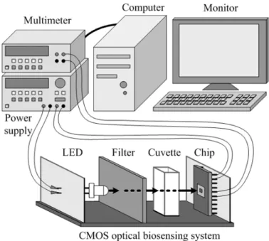
Figure 2-2: The diagram of the miniature CMOS optical biosensing system and the experimental setup.
contribute to the photocurrent, the shallower P+/N
well junction (about 0.2- m deep) was
adopted in this study to accomplish a better responsivity. (N+/Pwell junction is an
alter-native.) Moreover, the interdigitated P+/N
well junctions was used to extend the depletion
regions near the surface and hence increase the photocurrent [25]. Each P+ stripe was 1- m wide with 4- m seperation between stripes, and the stripes were interconnected by metal lines and contacts. The total area of this …nger photodiode was 100 m 100 m. The photodiode was surrounded by double guard rings to keep the substrate noise o¤; the P+ guard ring was connected to ground, and the N+ guard ring was connected to a high potential [26].
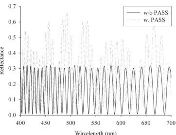
In a standard CMOS technology, the dielectric layers above the active region com-prise an inter-layer dielectric layer, inter-metal dielectric layers, and optional passivation layers (PASS). For a multi-layer structure, the re‡ectance can be calculated by using the impedance-transformation approach [27]. The e¤ective wave impedance Zi at the front
of the ith layer is expressed as
Zi = i
Zi+1+ j itan(kidi) i+ jZi+1tan(kidi)
(2.6)
Figure 2-3: The top view and cross section of P+/N
Figure 2-4: The calculated re‡ectance as a function of wavelength for the device with and without passivation layers.
of the ith layer, respectively; Zi+1 denotes the e¤ective impedance at the front of the
(i + 1)th layer. This recursive calculation starts from the known impedance of the last layer (silicon substrate), Zlast = Si, backward to the e¤ective impedance at the front of
the surface layer, Z1. Then the re‡ectance R of the photodiode can be obtained as
R = Z1 0 Z1+ 0
2
(2.7) where 0 is the intrinsic impedance of air. For the device with and without PASS, the
simulation results of the wavelength-dependent re‡ectance are shown in Figure 2-4. By removing PASS above the active region of the photodiode, simulation results show that the re‡ectance can be reduced from 0.169 to 0.116 for the 430-nm light, and from 0.481 to 0.006 for the 650-nm light.
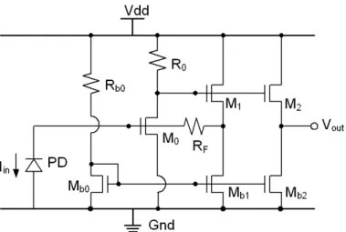
As shown in Figure 2-5, the subsequent circuit included a current source, a current mirror, a TIA, and an output bu¤er. The TIA consisted of a common-source stage M0,
two source followers M1 and M2, and an external feedback resistance RF. M1 served in
the feedback loop to isolate R0 from the loading e¤ect, and M2 drove the load capacitance
to alleviate the stability issue [28]. The gain of the TIA is given as
AT =
RFgm0R0
1 + (RFgm0R0)=RF ' R
Figure 2-5: The con…guration of the subsequent circuit. Device parameters are M0 = (100
m=0:5 m), M1 = M2 = (50 m=0:5 m), Mb0= Mb1 = Mb2= (1 m=0:5 m), R0 = 8
k , and Rb0= 15 k .
where gm0 is the transconductance of M0; gm0R0 was designed large enough to make AT
approximated to RF. The external RF allowed us to adjust the ampli…cation factor and
the dynamic range of the TIA. The input-referred noise current of the TIA is given as
I2 n;in = 4kT RF + 4kT R2 F gm0 + 1 g2 m0R0 + g2 m0gm1R20 (2.9)
where gm1 is the transconductance of M1, and is the excess noise coe¢ cient [28]. The
input-referred noise current were reduced by enlarging gm0, gm1, R0, and RF. In addition,
to prevent the above-mentioned circuits from illumination, these regions were covered with ‡oating metals as optical masks.
2.2.4
Biosensing System Setup
The diagram of the proposed CMOS optical biosensing system is illustrated in Figure 2-2. A narrowband LED is used as the light source, and a bandpass …lter allows the light of a speci…c wavelength to travel through the cuvette, in which the light is partially absorbed by the biochemical materials. The light after passing through the cuvette is detected by the CMOS biochip, which is mainly composed of a photodetector and a transimpedance ampli…er (TIA). The photodetector converts the transmitted optical signals into current signals, and then the TIA converts them into voltage signals. The voltage signals are measured by a multimeter (Agilent 34401A), which is connected to a personal computer
via a general purpose interface bus (GPIB), and an application software (Labview) is used for data acquisition.
2.2.5
Preparation of Biochemical Reagents
The biochemical experiments were assisted by Prof. Yuh-Shyong Yang’s group. ABTS (10 mg/tab), H2O2 (30%, W/W), HRP (250 U/mg), -D-glucose, histamine, and
DAO from porcine kidney (0.06 U/mg) were purchased from Sigma. GOx from Aspergillus Niger was purchased from Fluka. Sodium phosphate powders (monobasic and dibasic) were obtained from J. T. Baker. Other chemical reagents were of analytical grade and were used without further puri…cation.
The HRP, GOx, and DAO stock solutions were prepared in a 100-mM phosphate bu¤er and were stored at -20 C. These stock enzyme solutions were melted in an ice bath just before use and were diluted with a pH 7.0 phosphate bu¤er. The activity assays of HRP, GOx/HRP, and DAO/HRP in the systems containing various concentrations of H2O2,
glucose, and histamine, respectively, were initiated by adding 1-ml colorimetry reagent (30-mM ABTS in a 100-mM phosphate bu¤er, pH 7.0). The reactions were performed at 25 C (for HRP and GOx/HRP) and 37 C (for HRP and DAO/HRP), respectively.
2.3
Experimental Results
2.3.1
Characteristics of the Whole System
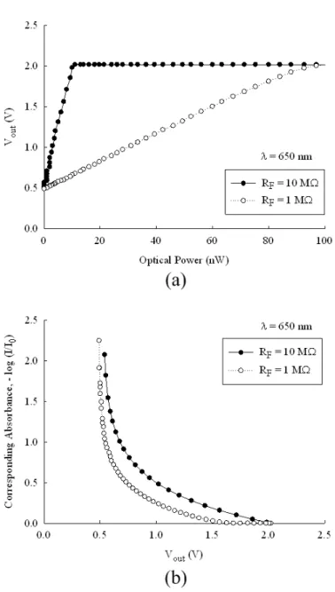
The biochip was manufactured using the TSMC (Taiwan Semiconductor Manufac-turing Company) 0.35- m CMOS technology. The die size (including the photodiode, core circuits, and I/O pads) is 1.35 mm 1.35 mm. The dimensions of the miniature biosensing system shown in Figure 1 are about 8 cm (length) 6 cm (width) 7 cm (height). The …nger photodiode was reverse-biased moderately to ensure that the pho-tocurrent was linearly proportional to the absorbed photons. The phopho-tocurrent was then converted into voltage signal by the subsequent TIA. With a 3-V power supply, the lower bound and upper bound of the output voltage were 0.49 V and 2.02 V, respectively.
Red LEDs (Centenary 31134) and a bandpass …lter (Onset 650FS10-50) were used to produce 650-nm light. When the biochip was illuminated, the output voltage Vout as a
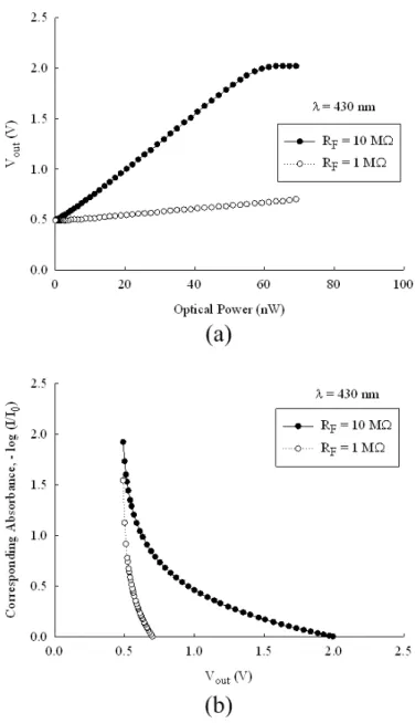
function of the input optical power for a 650-nm wavelength is shown in Figure 2-6(a). For RF =10 M and 1 M , the sensitivities were approximately 145 V/ W and 16 V/ W,
respectively. But the output voltage Vout for RF =10 M would saturate at 2.02 V when
the input optical power was larger than 10 nW. Combining the results of the linear region with (2.1) gives the corresponding relationships between the absorbances and the output voltages for two di¤erent RF’s, as shown in Figure 2-6(b). These relationships would be
bene…cial for the analysis of biochemical experiments since the absorbance of the material is proportional to the target’s concentration.
Similarly, purple LEDs (Centenary 40327) and a bandpass …lter (Newport 20BPF10-430) were used to produce 430-nm light. When the biochip was illuminated, the output voltage as a function of the input optical power for a 430-nm wavelength is shown in Figure 2-7(a). For RF =10 M and 1 M , the sensitivities were approximately 26 V/ W
and 3 V/ W, respectively. The output voltage Vout for RF =10 M would saturate at
2.02 V when the input optical power is larger than 60 nW. The relationships between the absorbances and the output voltages for two di¤erent RF’s are shown in Figure 2-7(b).
The measurement results of the CMOS chip indicate that the sensitivity of 650-nm light is higher than that of 430-nm light. But from the perspective on the biochemical product ABTS+, the absorption of 430-nm light is stronger than that of 650-nm light.
Accordingly, for comparison, the following biochemical experiments were performed with 650-nm light and 430-nm light individually.
2.3.2
H
2O
2Detection
The biochemical equation of the ABTS/H2O2/HRP method is expressed in Equation
(2.3). When the substrate ABTS and the enzyme HRP are su¢ cient, the amount of the product ABTS+ would be proportional to the H
2O2 concentration. For the experiment
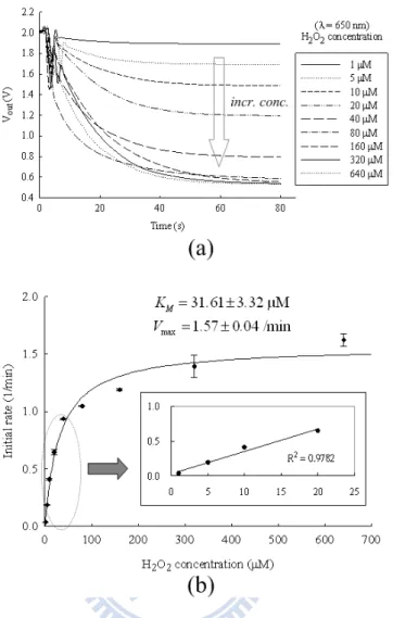
performed using 650-nm light and RF = 1 M , Figure 2-8(a) illustrates the real-time
measured voltages Vout under various H2O2 concentration, with an arrow indicating the
trend of increasing concentration (incr. conc.). The minimum H2O2 concentration was
successfully detected as 1 M, which is one order of magnitude better than the limit re-ported in previous literatures (about 50 M) [4], [5], and is even comparable to the limit obtained from a commercial spectrophotometer (Hitachi U-3310). With the relationship depicted in Figure 2-6(b), the absorbance at each time point for various H2O2
concen-Figure 2-6: Experimental results of the CMOS optical biosensing system with RF = 10
M and RF = 1 M at = 650 nm. (a) The output voltage versus the input optical
Figure 2-7: Experimental results of the CMOS optical biosensing system with RF = 10
M and RF = 1 M at = 430 nm. (a) The output voltage versus the input optical
Figure 2-8: Experimental results of the H2O2 detection with 650-nm light at 25 C. (a)
Real-time measurement of the output voltage for t = 0–80 s. (b) The Michaelis-Menten plot.
tration can be obtained. The Michaelis-Menten plot of H2O2 concentration is shown in
Figure 2-8(b), where the Michaelis constant Km = 20:22 3:31 M was computed by
using a nonlinear regression program (SigmaPlot). For a small [H2O2], the experimental
results demonstrate a good linearity with the coe¢ cient of determination R2 = 0:9782,
as shown in the inset of Figure 2-8(b).
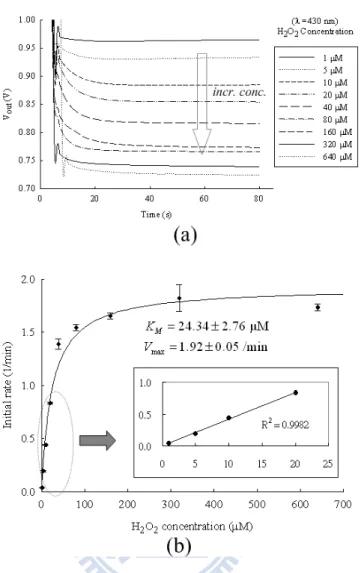
Similarly, for the experiment performed using 430-nm light and RF = 10 M , Figure
2-9(a) illustrates the real-time measured voltages Vout under various H2O2 concentration.
The minimum H2O2 concentration was successfully detected also as 1 M. With the
relationship depicted in Figure 2-7(b), the absorbance at each time point for various H2O2 concentration can be obtained. The Michaelis-Menten plot of H2O2 concentration is
Figure 2-9: Experimental results of the H2O2 detection with 430-nm light at 37 C. (a)
Real-time measurement of the output voltage for t = 0–80 s. (b) The Michaelis-Menten plot.
results demonstrate a good linearity with R2 = 0:9982 as shown in the inset of Figure
2-9(b).
2.3.3
Glucose Detection
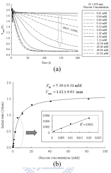
The coupled enzymatic reactions for glucose detection are expressed in (2.3) and (2.4). Su¢ cient ABTS, HRP, and GOx would ensure that the absorbance of the material is proportional to the glucose concentration. For the experiment performed using 650-nm light and RF = 1 M , the real-time measured voltages Vout under various glucose
concentrations are illustrated in Figure 2-10(a). The minimum glucose concentration was successfully detected as 10 M. The Michaelis-Menten plot of glucose concentration is
Figure 2-10: Experimental results of the glucose detection with 650-nm light at 25 C. (a) Real-time measurement of the output voltage for t = 0–200 s. (b) The Michaelis-Menten plot.
shown in Figure 2-10(b), where Km = 4:87 0:99 mM. In order to detect a lower glucose
concentration, the experiment was then performed using RF = 10 M . The obtained
Michaelis-Menten plot is shown in the inset of Figure 2-10(b), where R2 = 0:9851, and
the detection limit of the glucose concentration was improved to 1 M. This detection limit is two orders of magnitude better than the limit reported in previous literatures (about 500 M) [4], [5], and is comparable to the limit obtained from a commercial spectrophotometer (Hitachi U-3310).
Figure 2-11: Experimental results of the histamine detection with 430-nm light at 37 C. (a) Real-time measurement of the output voltage for t = 0–1200 s. (b) The Michaelis-Menten plot.
2.3.4
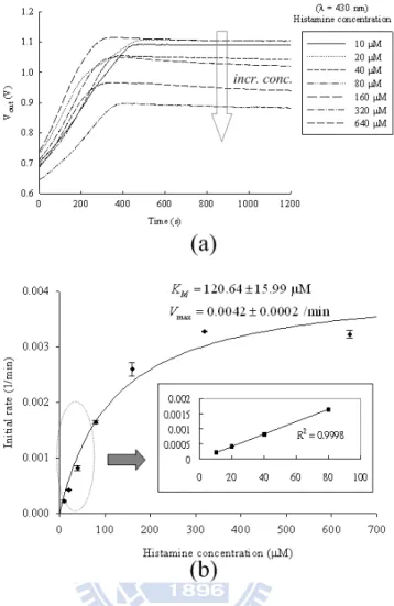
Histamine Detection
The coupled enzymatic reactions for histamine detection are expressed in Equations (2.3) and (2.5). Su¢ cient ABTS, HRP, and DAO would ensure that the absorbance of the material is proportional to the histamine concentration. For the experiment performed using 430-nm light and RF = 10 M , the real-time measured voltages Vout under various
histamine concentrations are illustrated in Figure 2-11(a). The minimum histamine con-centration was successfully detected as 10 M, which is comparable to the limit obtained from a commercial spectrophotometer (Hitachi U-3310). The Michaelis-Menten plot of histamine concentration is shown in Figure 2-11(b), where Km= 125:04 30:17 M. For
a diluted histamine solution, the experimental results demonstrate a good linearity with R2 = 0:9998 as shown in the inset of Figure 2-11(b).
2.3.5
Interfering Agents
For the ABTS/H2O2/HRP system, although HRP, GOx, and DAO are highly speci…c
enzymes, some chemicals in the blood may a¤ect the H2O2 detection. Among the possible
interfering agents in the blood, uric acid and acetaminophen were observed to have limited e¤ects on the H2O2 detection, whereas ascorbic acid (AA) would somewhat a¤ect the
H2O2 detection [29]. For healthy adults, the physiological concentration of AA in the
blood is about 60 M, and the glucose concentration in the blood is about 3–8 mM [30], i.e. the ratio of [AA] to [H2O2] is about 0.01. Since the sensitivity of our system for
glucose detection is in the low M range, the blood sample could be diluted to a 10 2 to
10 3 concentration for detection.
To investigate the e¤ects of AA upon the ABTS/H2O2/HRP system, the experiments
were performed using 10 M H2O2and various AA concentrations in the reaction mixture.
The activity of HRP was determined using the system with 650-nm light and RF = 1M ,
and the experimental results are shown in Figure 2-12. For [H2O2] = 10 M and [AA] < 1
M, the variation in the absorbance A of the reaction mixture was negligible. For [H2O2]
= 10 M and [AA] > 3 M, the signi…cant interference with the ABTS/H2O2/HRP system
due to the large AA concentration can be observed. However, when the diluted blood sample of a healthy adult is used in our detection system, the ratio of [AA] to [H2O2] is
about 0.01 and the expected AA concentration is much less than 1 M. Therefore, the interference from AA is also negligible for the blood examination.
2.4
Summary
An optical biosensing system based on a standard CMOS technology and absorption photometry has been presented. The whole system was assembled into a compact pro-totype, in which the CMOS biochip composed of a photodiode and a TIA demonstrated a high sensitivity and linearity. The quantum e¢ ciency of the P+/Nwell photodiode was
enhanced by adopting the interdigitated structure and removing the passivation layers in the CMOS structure. In addition, the switchable feedback resistance of the TIA allowed a user to adjust the ampli…cation factor and the dynamic range for examining di¤erent concentration levels of an analyte. The ABTS/H2O2/HRP method was introduced as a
Figure 2-12: The absorbance A of the reaction mixture versus the AA concentration. (a) At low concentration. (b) At high concentration.
that produce H2O2. The experimental results reveal that the detection limits of H2O2,
glucose, and histamine concentration are 1 M, 1 M, and 10 M, respectively. The detection limits are at least one order of magnitude better than those of reported CMOS biosensors, and are even comparable to those of a commercial spectrophotometer.
The whole system exhibits a high detection capability, a large dynamic range, a high reproducibility, a short response time, and a low sample volume requirement. Therefore, the development of this CMOS biosensing system is a stepping stone toward a portable, reliable, inexpensive, and convenient home care instruments. In the future, more ad-vanced functions such as rapid screening and automatic monitoring could be realized, and a practical miniature instrument for personalized clinical diagnosis may be reason-ably expected.
Chapter 3
Ring-Shaped Phototransistors for
Biomedical Applications
3.1
Introduction
A conventional CMOS photodiode can easily be formed by utilizing a single N+/P well,
P+/N
well, or Nwell/Psub junction, but the responsivity is low [1]. Avalanche multiplication
is a way to bring an internal current gain. However, the demand for high bias voltage also limits its use in many applications. Circumventing this di¢ culty, a CMOS phototransistor could have a current ampli…cation under moderate bias through the internal transistor action [31].
In this research, a high-sensitivity phototransistor manufactured in a standard CMOS technology is proposed [32]. Based on this phototransistor, a miniature optical biosensing system is developed. The optoelectronic measurements and biochemical experiments are also presented.
3.2
Principles and Methods
3.2.1
Absorption Photometry
The absorbance A of the materials is described by the Beer-Lambert law [6]
A = log I I0
where I0 and I respectively denote the initial light intensity and the light intensity after
passing through the material, is the wavelength-dependent molar absorptivity in units of l mol 1 cm 1, l is the path length in units of cm, and c is the concentration of absorbing
species in the material in units of M (1 M = 1 mol l 1). When the light source and the
path length are …xed, the absorbance would be proportional to the analyte concentration. Therefore, detecting the optical signals modulated by the biochemical reactions is an e¢ cient way to quantitate the analyte of interest.
Regarding a commercial spectrophotometer, the used sample volume and the path length are about 1 ml and 1 cm, respectively. Referring to (3.1), when a shorter path length is used, the change in the absorbance becomes smaller, which makes the detection of concentration more di¢ cult. For a miniature system, in order to further reduce the sample volume as well as the path length, the development of a high-sensitivity optical sensor is of great importance.
3.2.2
Biochemical Reaction
Horse-radish peroxidase (HRP) is a popular enzyme that has been widely used in bio-chemical applications. While an antibody is used to recognize a target protein of interest, HRP can be conjugated to the antibody to serve as a label for determining the amount of the target [33]. HRP is usually used combining with hydrogen peroxide (H2O2) to oxidize
an added substrate that is luminescent or chromogenic. Reported optical methods for HRP detection include the luminol/H2O2/HRP reaction [4], the ABTS/H2O2/HRP
reac-tion [21], and the TMB/H2O2/HRP reaction [34]. The end products of these reactions
can either emit or absorb the light of speci…c wavelengths for analysis.
The TMB/H2O2/HRP reaction is adopted as the basis for biomedical applications in
our system. TMB stands for 3,3’,5,5’-tetra-methyl-benzidine. It is neither mutagenic nor carcinogenic [35] and is a widely used reagent for ELISA (enzyme-linked immuno-sorbent assay).
The oxidation of TMB by H2O2 with HRP can be easily observed for qualitative
analysis. The reactant solution is visually light green, whereas the soluble end product is deep blue. After the addition of sulfuric acid (H2SO4) to the media, this reaction would
Figure 3-1: The top view and cross section of the PMOS phototransistor.
TMB — — — — –> TMBH2O2+ HRP + — — — > TMBH2SO4 2+ (3.2) For quantitative analysis, the analyte concentration can be evaluated by detecting the optical absorbance of the solution. The absorption spectra obtained from a standard spectrophotometer (Hitachi U-3310) show that the reactant TMB has an absorption peak at 280 nm, whereas the blue product TMB+ has absorption peaks at 370 nm and 650 nm. With the presence of H2SO4, the yielded yellow product TMB2+ has an absorption peak
at 450 nm.
3.2.3
Ring-Shaped Phototransistor
The top view and cross section of the proposed PMOS phototransistor are shown in Figure 3-1. The P+ source placed in the center is surrounded by the polysilicon gate and the P+drain, while the N
well bulk (B) is enclosed by the Pwell ring (R). It can be regarded
as a PMOS with a photodiode connected across the bulk (B) and the square ring (R). The PMOS phototransistor leaves the Nwell bulk ‡oating and uses the Nwell/Psub
junc-tion diode for the optical access [38]. The photogenerated carriers driftting into the Nwell
output drain current.
The output drain current ID of a MOSFET operated in the saturation region can be
expressed as ID = 1 2 W L Cox(VGS VT) 2 1 + VDS VA (3.3) where W , L, , Cox, VGS, VT, VDS, and VA are the channel width, the channel length,
the carrier mobility, the oxide capacitance per unit area, the gate-source voltage, the threshold voltage, the drain-source voltage, and the Early voltage, respectively [31]. The shift amount of the threshold voltage due to the bulk charge e¤ect is given by
VT = p 2"sqNB Cox p 2 B+ VSB p 2 B (3.4)
where "s, q, NB, and B are the permittivity of silicon, the unit electric charge, the
doping concentration of the bulk, and the bulk Fermi level from the intrinsic Fermi level, respectively; VSB is the source-bulk voltage resulting from the optical access.
Using the proposed layout style, the sensing area of the outer ring photodiode is enlarged, so as to cause a larger shift amount of the threshold voltage. The channel length is also smaller than that of a conventional PMOS with the same area. Since the output drain current is inversely proportional to the channel length, a larger photocurrent response could be expected.
3.2.4
Biosensing System Setup
The proposed PMOS phototransistor with area of 100 m 100 m was man-ufactured using the TSMC (Taiwan Semiconductor Manufacturing Company) 0.35- m standard CMOS technology. The photograph and the illustrated diagram of the whole biosensing system are shown in Figure 3-2, and its dimensions are about 7 cm (length) 5 cm (width) 5 cm (height). A red LED (Centenary 31134) is used as the light source, and a slide is placed above the PMOS phototransistor to hold the biochemical sample. A sample volume of only 10 l is required for the detection. The path length l through the sample is about 0.1 cm.
The light travelling through the sample is partially absorbed and then detected by the PMOS phototransistor, which converts the transmitted optical signals into current signals. The current signals are measured using a precision semiconductor parameter
Figure 3-2: The phototransistor-based biosensing system: (a) photogragh and (b) illus-trated diagram.
analyzer (HP 4156A), which is connected to a personal computer via a general purpose interface bus (GPIB). An application software (Interactive Characterization Software, ICS) is used for data acquisition.
3.2.5
Preparation of Biochemical Reagents
The biochemical experiments were assisted by Prof. Yuh-Shyong Yang’s group. TMB liquid substrate system, HRP-streptavidin, and phosphate bu¤ered saline (PBS) powders were purchased from Sigma. Other chemical reagents were of analytical grade and used without further puri…cation.
The HRP stock solutions (1 g/ l) were prepared in a PBS bu¤er and stored at 20 C. The stock enzyme solutions were melted in an ice bath just before use and diluted with double distilled water (ddH2O). The reactions were performed at 25 C.
Figure 3-3: The measured I-V charateristics of the PMOS phototransistor.
3.3
Experimental Results
3.3.1
Device Characteristics
While the proposed PMOS phototransistor was without illumination, the measured I-V characteristics are shown in Figure 3-3. The bias conditions were as follows: the source was grounded, the drain voltage swept from 0 V to 3V, the gate voltage stepped from 0 V to 3 V, the bulk was ‡oating, and the ring voltage was …xed at 3V. It can be seen that for VDS = 3 V, the phototransistor was operated in the saturation region.
The larger jVGSj was, the larger jIDSj was.
While the phototransistor was illuminated, the output drain current varied in response to the light intensity. For VDS = 3V, the measured photocurrent responses under
vari-ous illumination intensities of 650-nm light are shown in Figure 3-4(a). The photocurrent response divided by illumination intensity can give the responsivity, and the results are shown in Figure 3-4(b). For VGS = 2 V and 3 V, the phototransistor exhibited a
responsivity higher than 1000 A/W. The responsivity is 2000 folds higher than that of a traditional silicon P/N junction photodiode (about 0.5 A/W) [2].
Even for very small bias voltages such as VDS = 0:1 V and VGS = 0 V, the
photo-transistor can successfully detected the change of illumination intensity and exhibited a responsivity of about 50 A/W.
Figure 3-4: The optoelectronic characteristics of the PMOS phototransistor for VDS = 3
V with various VGS: (a) photocurrent response versus illumination intensities and (b)
Figure 3-5: The photocurrent response versus HRP concentration for VDS = 3 V with
various VGS.
dark current were observed to examine the device stability. For VDS = 3 V and VGS =
2 V, the drift amount of dark current after four months was 29.2 A, which is much smaller than the amplitude of photocurrent response (at least hundreds A). For VDS =
0:1 V and VGS = 0 V, the drift amount of dark current after four months was 0.75 nA,
which is also much smaller than the amplitude of photocurrent response (at least hundreds nA). Hence the stability of the proposed PMOS phototransistor could be acceptable.
3.3.2
HRP Detection
The system setup is illustrated in Figure 3-2. A sample volume of only 10 l was required to be dropped on the slide above the phototransistor. For the experiments per-formed using 650-nm light with di¤erent HRP concentrations, the measured photocurrent responses for VDS = 3V with various VGS are shown in Figure 3-5. The used HRP
con-centration values were 0.0, 2.7, 5.3, 13.3, 26.6, 53.2, and 212.8 pM, respectively. Each data point is the average of …ve measurement results.
For VDS = 3V and VGS = 2V, the highest sensitivity of 2.5 A/pM was achieved,
and the linear relationship ranged from 2.7 pM to 212.8 pM with the coe¢ cient of de-termination R2 = 0:9990 calculated by an application software (Microsoft Excel). The
statistical information of the photocurrent response Iph is summarized in Table 3.1. For
Figure 3-6: The measured I-V characteristics for VGS = 0 V under various HRP
concen-trations.
the 2.7-pM solution, the Iph mean is 893.2 A and the standard deviation is 2.510 A.
Since the di¤erence in the Iph mean is much larger than the standard deviation, the
ex-perimental results indicated that the minimum HRP concentration successfully detected was 2.7 pM. This detection limit is three orders of magnitude better than that of a lately reported silicon biosensor (2.4 nM) [11], and is even comparable to the limit obtained from a commercial spectrophotometer (Hitachi U-3310). The required sample volume of our system is also smaller.
For VGS = 0 V, the phototransistor can still be used for biochemical detection, and
the measured I-V characteristics under various HRP concentrations are shown in Figure 3-6, with an arrow indicating the trend of increasing concentration. When the HRP concentration is increasing, the color of the end product become darker, which implies that more light will be absorbed, and thus the output drain current become smaller and closer to the condition in a darkroom. Even for very small bias voltages such as VDS = 0:1 V,
the experimental results shown in Figure 3-7 also demonstrated a detection limit of 2.7 pM. The di¤erence in Iph mean between the bu¤er and 2.7-pM solution is 3.1 A, which
is much larger than the standard deviation of 0.1 A.
To investigate the corresponding absorbances for various HRP concentration solutions, …rstly the relationship between the absorbance and the photocurrent response can be obtained by combining (2.1) and Figure 4(a), and the results are shown in Figure 3-8(a). Then combining Figure 3-5 and Figure 3-8(a) gives the relationship between the absorbance and HRP concentration. For VDS = 3 V and VGS = 2 V, the obtained
Figure 3-7: The photocurrent response versus HRP concentration for VDS = 0:1 V and
VGS = 0 V.
Table 3.1: The statistical information of the photocurrent response Iphand the absorbance
A for VDS = 3 V and VGS = 2V under various HRP concentration.
Iph ( A) Absorbance
Conc. (pM) mean SD mean SD bu¤er 901.0 1.140 -0.004 0.002 2.7 893.2 2.510 0.017 0.005 5.3 879.2 1.140 0.054 0.002 13.3 857.4 1.643 0.113 0.004 26.6 826.8 1.924 0.195 0.004 53.2 770.8 1.304 0.346 0.003 218.8 414.8 3.194 1.302 0.007 darkroom 0.0 1.342 2.417 0.003 (Conc.: concentration, SD: standard deviation)
results show that the linear detection range was from 2.7 pM to 212.8 pM with R2 =
0:9991, which is depicted in Figure 3-8(b). The statistical information of the absorbance A is summarized in Table 3.1.
3.4
Applications for Screening Skin-Whitening Agents
3.4.1
Motivation
In recent years, abundant candidates of skin whitening agents have been developed. To screen the e¢ ciency of these whitening agents, much attention has been devoted to the development of convenient biosensors.
Figure 3-8: The corresponding absorbance versus (a) photocurrent response and (b) HRP concentration.
increase their production of melanin in response to sun exposure, and that would lead to freckles. For skin-whitening agents, the mechanism of melanogenesis suppression could be divided into two categories: the inhibition of melanin production pathway and the decrease of melanocyte proliferation [39], [40].
In this research, three major methods for evaluating e¤ects of skin whitening agents were applied: melanin, MTT, and tyrosinase assays. The schematic diagram of these assays are shown in Figure 3-9. Melanin assay is related to content of melanin prod-uct; MTT assay is related to viability of melanoma cells; tyrosinase assay is related to tyrosinase activity.
3.4.2
Materials and Methods
Melanin Assay
Murine melanoma B16-F10 cells (ATCC: CRL-6475) were cultured in DMEM (Dul-becco’s modi…ed Eagle’s medium) with 10% heat-inactivated fetal bovine serum, 1.5-g/L sodium bicarbonate, 4.5-g/L glucose, and 1% antibiotics. The cells were seeded in 6-well
Figure 3-9: The schematic diagram of three major assays for evaluating whitening agents.
plates at densities of 2 105, 1 105, 5 104, and 2.5 104 cells/ml, respectively. After
the incubation in a 5% CO2 incubator at 37 C for 5 hours, cells were digested by 0.25%
(w/v) trypsin with 0.52-mM EDTA solution (GIBCO), and washed with PBS (phosphate-bu¤ered saline). Then the supernatant was discarded, and cells were lysed in 200- l 1-N NaOH at 80 C for 1 hour. To evaluate the density of cells, the optical absorbance was measured using the CMOS biosensor.
MTT Assay
Murine melanoma B16-F10 cells were cultured and seeded in 6-well plates at several densities. After the incubation in a 5% CO2incubator at 37 C for 5 hours, 800- l 1-mg/ml
MTT [3-(4,5-dimethylthiazol-2-yl)-2,5-diphenyltetrazolium-bromide] solution freshly pre-pared in PBS was added to each well of cells cultured plate. The cells were incubated at 37 C for 4 hours, and then 800- l DMSO (dimethyl sulfoxide) was added to each well to dissolve the purple MTT-formazan. After the incubation at 37 C for 10 minutes, the optical absorbance was measured using the CMOS biosensor.
Tyrosinase Assay
Murine melanoma B16-F10 cells were cultured and seeded in 6-well plates at several densities. After the incubation in a 5% CO2 incubator at 37 C for 3 days, cells were
digested by 0.25% (w/v) trypsin with 0.52-mM EDTA solution (GIBCO), and washed with PBS (phosphate-bu¤ered saline). Then the supernatant was discarded, and cells were lysed in 150- l 0.1-M sodium phosphate bu¤er (pH6.8) containing 1% Triton X-100 and 0.1-mM PMSF. Then cells were frozen at -20 C for 30 minutes. After thawing and mixing, cellular extracts were clari…ed by centrifugation at 12000 rpm for 30 minutes at 4 C. The 80- l supernatant and 20- l 2-mg/ml L-DOPA were placed in 96-well plates. Speci…c activity was de…ned as the amount of L-dopaquinone formed per cell. Following the incubation at 37 C, the optical absorbance was measured using the CMOS biosensor.
Absorption Photometry
The analyte concentration can be quantitated by detecting the optical absorbance of the product solution. The absorption spectra obtained from a spectrophotometer (Hitachi U-3310) show that the products for melanin assay, MTT assay, and tyrosinase assay have absorption peaks at 470 nm, 520 nm, and 550 nm, respectively.
System Setup
The top view and cross section of the proposed CMOS phototransistor are shown in Figure 3-1, and the illustrated diagram and the photograph of the whole biosensing system are shown in Figure 3-2. A green LED (Centenary 36341) with a peak at 520 nm is used as the light source, and a slide is placed above the CMOS phototransistor to hold the biochemical sample. Only a sample volume of 10 l is required for the detection. The path length through the sample is about 0.1 cm
3.4.3
Experimental Results
Melanin Assay
The experimental Id-Vdcurves of the phototransistor for measuring the melanin assay
are shown in Figure 3-10, in which NaOH represents the reference condition without melanocytes. The results indicate that the density of 5 104 cells/ml can be successfully
Figure 3-10: The measured Id-Vd curves for the melanin assay.
MTT Assay
The measured Id-Vd curves for the MTT assay is shown in Figure 3-11. DMSO is
used as the reference without melanocyte. It indicates that the density of 5 104 cells/ml
can be successfully detected.
Tyrosinase Assay
The measured Id-Vd curves for the tyrosinase assay is shown in Figure 3-12. H2O is
used as the reference without melanocyte. It indicates that the density of 5 104 cells/ml can be successfully detected.
Kojic Acid E¤ect
Kojic acid is a well-known standard in skin whitening used to evaluate the potency of a new drug candidate. This whitening agent can inhibit the tyrosinase activity and reduce the melanin content without in‡uencing the proliferation of B16-F10 cells. The e¤ects of Kojic acid on these three assays was determined at di¤erent concentrations, as shown in Figure 3-13.
Figure 3-11: The measured Id-Vd curves for the MTT assay.
Figure 3-13: The e¤ects of Kojic acid on B16-F10 cells for melanin, MTT, and tyrosinase assays.
3.5
Applications for Ultra-Violet Detection
3.5.1
Motivation
The development of a photodetector with high responsivity for the UV/blue spectral range has attracted much interest for many applications [8], [21], [41], [42]. For bio-chemical analysis, the detection of the optical properties changed by bio-chemical reactions is a competent approach to examine various important biological molecules. Through the chemical reactions, the change of the emitted- or absorbed-light intensity is generally less than 1 W. Regarding the reported methods, the luminol/H2O2/HRP reaction
in-volves the emission of 425-nm light [8], and the ABTS/H2O2/HRP reaction involves the
absorption of 415-nm light [21].
Much work has been devoted to the realization of photodetectors using a standard CMOS technology or CMOS-compatible technologies in the last decade [41]–[49]. The responsivity of a conventional CMOS photodiode for the UV/blue spectral range is low (about 0.2 A/W) [2]. Circumventing this drawback, a phototransistor can have a current ampli…cation under moderate bias through the internal transistor action [31]. However, little work has been conducted on the phototransistor manufactured using a standard CMOS technology for the UV/blue spectral range.
In this research, the proposed CMOS phototransistor exhibited an enhanced respon-sivity for the UV/blue spectral range.
Figure 3-14: The top view, cross section, and equivalent symbol of the proposed (a) PMOS phototransistor and (b) NMOS phototransistor.
3.5.2
Operating Principle
The device structures of the proposed PMOS and NMOS phototransistor based on CMOS technology are shown in Figs. 3-14(a) and 3-14(b), respectively. For the PMOS phototransistor, the P+ source is placed in the center with the ring-shaped poly-silicon
gate and P+drain, while the N
well bulk (B) is enclosed by the Pwell ring (R). For the NMOS
phototransistor, the N+ source is placed in the center with the ring-shaped poly-silicon
gate and N+ drain, while the P
well bulk (B) is enclosed by the Nwell ring (R). In both
cases, the phototransistor can be regarded as a MOSFET with a photodiode connected across the bulk (B) and the square ring (R), as shown in Figure 3-14.
Serving as an optical sensor, the phototransistor leaves the bulk ‡oating and mainly uses the Nwell/Pwell junction to separate photogenerated electron-hole pairs [46]. The
pho-togenerated carriers drifting into the bulk would change the bulk potential, and thereby change the threshold voltage as well as the output drain current.
For the UV/blue incident light, most photogenerated carriers are very close to the surface (within 0.2 m). Using the proposed ring-shaped layout style, the near-surface depletion region of the outer Nwell/Pwell ring-shaped photodiode is enlarged and superior
to that of a conventional MOSFET with the same area, so as to cause a larger shift amount of the threshold voltage. Hence a larger photocurrent response Iph could be expected.
Regarding the proposed phototransistors, the bulk is left ‡oating, while the applied …xed ring-source voltage VRS is negative for PMOS and is positive for NMOS. The
bulk-ring voltage VBRresulting from the illumination can be described by the transposed diode
equation [31] VBR = Vthln 1 + IBR(ph) IBR0 = Vthln 1 + k1Popt IBR0 (3.5) where Vth, IBR(ph), IBR0, and Popt are the thermal voltage, the photocurrent of the
bulk-ring diode, the saturation current of the bulk-bulk-ring diode, and the incident optical power density, respectively; k1 is functions of material parameters, transistor bias voltages, and
the depletion region area of the Nwell/Pwell junctions. Thus the resulted bulk-source
voltage VBS can be expressed as VBS = VBR + VRS. For illuminated PMOS, VBS is
negative since its Nwell bulk accumulates excess electrons; for illuminated NMOS, VBS is
positive since its Pwell bulk accumulates excess holes.
The shift amount of the threshold voltage VT due to the bulk charge e¤ect is given
by [31] VT = p 2"sqNB Cox p 2 B VBS p 2 B (3.6)
where "s, q, NB, Cox, and B are the permittivity of silicon, the unit electric charge, the
doping concentration of the bulk, the oxide capacitance per unit area, and the bulk Fermi level from the intrinsic Fermi level, respectively. When PMOS and NMOS phototransis-tors are illuminated, the absolute value of the threshold voltage jVTj will both become
smaller.
The photocurrent response Iph is the di¤erence in the output drain current, which can
be expressed as
Iph =jID ID0j (3.7)
where ID and ID0denote the output drain current of the phototransistor with and without
illumination, respectively. It implies that Iph of the phototransistor will increase with the
Nwell/Pwell sensing area A, the channel aspect ratio W=L, and the bias voltages jVGSj and
jVDSj.
Figure 3-15: The measured I-V characteristics of the PMOS phototransistor without illumination.
the proposed CMOS phototransistor is expected to perform a better responsivity than conventional CMOS-based photodetectors.
3.5.3
Experimental Results
The proposed PMOS and NMOS phototransistors were respectively duplicated and concatenated to form each 10 10 array with a total area of 100 m 100 m, and they were manufactured using the TSMC (Taiwan Semiconductor Manufacturing Company) 0.35- m standard CMOS technology. To characterize these phototransistors, a UV/blue LED (Centenary 40327) with the peak of 400 nm was used as the light source, while its light intensity was adjusted by a power supply (Agilent E3631A). A reference photodetec-tor and a pinhole were introduced to measure the optical power density for various bias voltages applied to the LED. A precision semiconductor parameter analyzer (HP 4156A) and a test …xture (HP 16058A) were used to characterize the CMOS photodetectors.
Figure 3-15 shows the measured I-V characteristics of the PMOS phototransistor without illumination. The bias conditions were as follows: the source was grounded, the drain voltage swept from 0 V to 3 V, the gate voltage stepped from 0 V to 3 V, the bulk was ‡oating, and the ring voltage was …xed at 3 V.
While the phototransistors were illuminated, the output drain current varied in re-sponse to the light intensity. For the PMOS phototransistor with jVDSj = 3 V, the
Figure 3-16: The optoelectronic characteristics of the PMOS phototransistor for VDS =
3V with various VGS: (a) photocurrent response versus illumination intensities and (b)