行政院國家科學委員會專題研究計畫 成果報告
系統晶片之靜電防護元件模擬、電路模型與參數最佳化之研
究(II)
計畫類別: 個別型計畫 計畫編號: NSC94-2215-E-009-084- 執行期間: 94 年 08 月 01 日至 95 年 07 月 31 日 執行單位: 國立交通大學電信工程學系(所) 計畫主持人: 李義明 報告類型: 精簡報告 處理方式: 本計畫可公開查詢中 華 民 國 95 年 10 月 23 日
行政院國家科學委員會補助專題研究計畫成果報告
※※※※※※※※※※※※※※※※※※※※※※※※※※
※
系統晶片之靜電防護元件模擬、電路模型與參數最佳化之研究(II)
※
※※※※※※※※※※※※※※※※※※※※※※※※※※
計畫類別:5個別型計畫 □整合型計畫
計畫編號:NSC 94-2215-E-009-084-
執行期間:
94 年 8 月 1 日至 95 年 7 月 31 日
計畫主持人:李義明
共同主持人:
計畫參與人員:
執行單位:
交通大學電信系中 華 民 國
95 年 10 月 20 日
系統晶片之靜電防護元件模擬、電路模型與參數最佳化之研究(II)
“Modeling, Simulation and Optimization of ESD Protection Designs for SOC era (II)” 計畫編號:NSC94-2215-E-009-084- 執行期間:94 年 8 月 1 日 至 95 年 7 月 31 日 主持人:李義明 交通大學電信工程系 副教授 一、 中文摘要 運用前一年研究的 ESD 元件模式與 ESD 電路模擬技術,本報告報導一個探討奈米電晶 體架構之靜電放電防護電路的 floating 電荷效 應之研究成果。藉由考慮新穎的全silicided N 型 MOSFETs,模擬與實驗顯示本研究探討的 靜電放電防護電路架構比傳統的silicided 技術 可以承受更好的 ESD 性能。適合解決電路緩 衝級的ESD 相關問題。 英文摘要
In this report, the floating charge effect is considered in the design of new full-silicided NMOSFETs for designing electrostatic discharge (ESD) protection circuit consisting of nanodevices. According to the designed, fabricated, and studied new full-silicided ESD protection nanodevices (e.g., 90 nm CMOS devices), our investigation demonstrates that there is a significant improvement in sustaining ESD robustness than that of the conventional full-silicided device. Furthermore, it has an excellent electrical efficiency than those of drain ballast resistor tied devices. Moreover, our novel design exhibits a higher driving current and better reliability without suffering the off states current of the fully-silicded devices. Those good characteristics are especially suitable for the output buffer design in which both driving capability and ESD robustness have to be considered.
二、 計畫的緣由與目的
Recently, the susceptibility of integrated circuits (ICs) to electrostatic discharge (ESD) has warranted the use of dedicated on-chip ESD protection circuits. Many attentions had been taken in solving the ESD issues; however, design of robust ESD circuits still remains challenging as critical devices dimensions continuously shrinking [1-3]. It is known that the operation speed of integrated circuit will be promoted faster and faster when the geometry of devices becoming smaller and smaller. Unfortunately, a high risk of the ESD damage has also been caused. The consequence is mainly resulted from the fact that a thinning down of gate-oxide will make the turn-on voltage of parasitic bipolar junction transistors (BJT) higher than the breakdown voltage of the gate-oxide; therefore, it increases the possibility of gate-oxide damage the during ESD stressing.
To enhance the robustness of the ESD protection circuit, the drain ballast resistors made from the silicide-blocked diffusion region has long been designed between the drain contacts and polysilicon gates [4-7]. However, this approach requires an additional photo-mask, enlarges the device’s area, and needs an extra device models in VLSI circuit design. The consequence will increase the process cost, lower devices density, and degrade the circuit performance. Therefore, a fully-silicded MOSFET device is an attractive candidate in
ESD protecting circuits. Unfortunately, it suffers a low ESD robustness [8-11]; in particular, for the sub-100 nm device era.
In this report, we propose a novel fully silicided MOSFET structure for robust ESD protection circuit design consisting of sub-100 nm devices. This alternative lets the body electrode in floating state under ESD stress. The experimental results show that the floating body effects reduce the turn on voltage, improve the ESD performance, and have a better robustness for sub-100nm device design. The test devices are fabricated with a standard CMOS process with a gate length of 90 nm and a gate-oxide thickness of 1.2 nm. The ESD characteristics are verified with the TLP systems with a pulse width of 100 ns [3,12-13]. It is found that the new fully silicided device has improved ESD robustness than the conventional one. Reliability of the new fully-silicided device is also taken into consideration. We find that the new device has a relatively better reliability than the conventional approach; moreover, the driving capability of the device is also enhanced. The achievement is significant and suitable for designing output buffer that all of the ESD strength, reliability and driving capability are important elements.
The improvement is caused from the accumulation of impact ionization holes that build up an electrostatic potential at the substrate; consequently, it decreases the turn on voltage of parasitic BJT. A decrement of turn on voltages will suppress the damage of gate oxide and reduces the electric fields at the drain junctions. We indicate that a wider current path exists in the new devices; as a result, the device sustains a better ESD strength than the conventional one does. A constructive alternative is also
demonstrated here for designing a fully-silicided ESD protection circuit. It exhibits an excellent efficiency on both ESD protection and chip area, and is very attractive to sub-100 nm CMOS circuit era. The report is organized as follow. In Sec. 2, we state the experimental characterization and report and discuss the results. Sec. 4 draws the conclusion. Input pad Core CKT Output pad Input ESD protection
Output buffer and ESD protection
Figure 1. The protection schematic used in the IC design. 三、 研究方法及成果
The fully-silicided and silicide-blocked devices are fabricated by using United Microelectronics Corporation (UMC) 90 nm CMOS technology. The manufacture process consists of: (1). Minimum feature size of the process is 90 nm; (2). The oxide thickness of the devices is 1.2 nm; (3). The silicide is formed by using two steps self-align cobalt silicide process that a 30 nm thick cobalt-silcide is formed selectively on the source, drain, and gate region; and (4). The drain ballast resistor is formed by using silicide-blocked process achieved by depositing a 100 nm thicken chemical vapor deposition oxide on the blocked regions prior to the formation of cobalt silicide. TLP measurement is done by using Barth Electronics Model 4002 TLP system. Pulse width of the measurement is 100n second that is highly correlated with the Human Body model (HBM). Finally, HP 4156B semiconductor analyzer does
the quasi-static characteristics of the devices. Accelerated test is performed by applying 3.3 V on both gate and drain electrodes of the device for over 20000 seconds. It should be noticed that the normal operation voltage of those devices is only about 1.2 V, thus we applied almost three times of the normal operation voltage at the accelerated tests. During the accelerated tests, the quasi-static IV characteristics are measured every 1000 seconds in calculating the transconductance (gm) degradation. Based on the numerical solution of a set of semiconductor device equations, the developed device simulator is applied to theoretically explain and investigate the floating charge effects in the proposed fully-silicided device [14-15]. The simulation model includes the Poisson equation, the electron-hole current continuity equations, the impact ionization, and the electron-hole energy conservation equations. p-well drain n+ n+ gate STIp+ p+ drai n body -con tact sour ce p-well drain n+ n+ gate STI STI n+ n+ drai n body -con tact sour ce (a) (b)
Figure 2. (a) A conventional full-silicided N-MOSFET. (b) The proposed full-silicided floating body NMOSFET.
p+ pi c k up n + s our c e n + s our c e n + s our c e n + s our c e n + s our c e n + s our c e n + s our c e n+ dr a in n+ dr a in n+ dr a in n+ dr a in n+ dr a in n+ dr a in gate n+ pi c k u p n+ s o ur c e n+ s o ur c e n+ s o ur c e n+ s o ur c e n+ s o ur c e n+ s o ur c e n+ s o ur c e n+ d ra in n+ d ra in n+ d ra in n+ d ra in n+ d ra in n+ d ra in gate (a) (b)
Figure 3. A top view of (a) the conventional and (b) the floating body full-silicided N-MOSFET.
The pMOSFET and nMOSFET pairs are most used ESD protection devices that prevent the input and output circuit from the ESD current damage. The protection schematic is shown on
Fig. 1 that nMOSFETs and pMOSFETs are tied between the input / output pads to ground line and power line, respectively. A more detailed observation could be drawn that the protection devices putted at the input pads are gate grounded structure for leakage suppression. On the other hand, the protection devices are always functioning as an output buffer at the output pads to have higher driving capability. According to the protection schematic, it will be summarized that an ideal protection device has to include several characteristics; those are the high ESD robustness, short response time, compatibility with the integration circuit process and high driving capability.
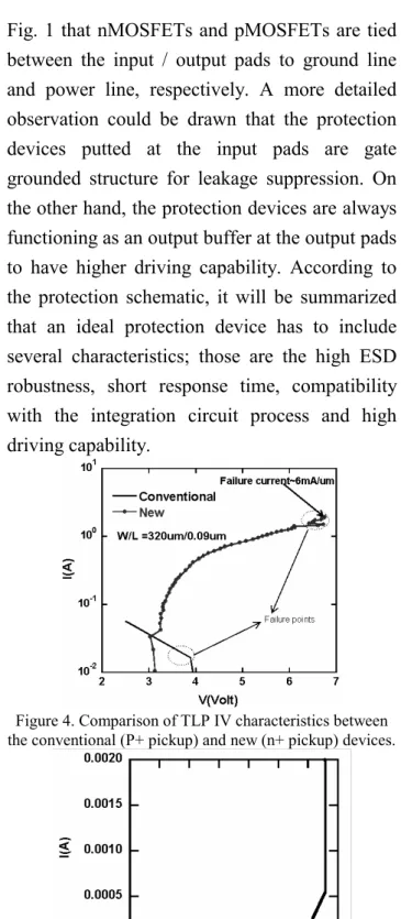
Figure 4. Comparison of TLP IV characteristics between the conventional (P+ pickup) and new (n+ pickup) devices.
Figure 5. The TLP IV characteristics of the thin oxides. In considering the ESD robustness, the fully-silicided devices conventionally do not be taken into ESD protection design for their low ESD robustness. This is mainly caused from the fact that gate-oxide and channel region should be
easily damaged for the over quantity of both current and voltage. Thus, in avoiding the undesired voltage and current distributions, the floating body design is taken into considerations in this work. The difference between the conventional fully-silicded and our proposed fully-silicded devices could be clearly found from the three-dimensional topological views shown in Figs. 2 and 3, respectively. The pickup design is the only difference between the conventional and our proposed device. That is the p+ pickup drawn for the conventional device and the n+ pickup designed for our proposal. The difference between the conventional and our proposed fully-silicded devices is small, but the difference of the ESD robustness between these two structures is significant. The improvement of our proposed device can be easily investigated from Fig. 4 that presents current vs. voltage (IV) characteristics measured from the TLP. A significant result is found that the floating body one sustains a much better ESD robustness than the grounding one. Shown in this figure, we can also demonstrate the problem of the conventional fully-silicided device that failure at the mean time of device turning on. With having the characteristic, we can conclude that an enlargement of device area will do nothing for the enhancement of ESD robustness. The results are highly matched with our theoretical analysis results.
The TLP IV curve of thin gate-oxide is shown in Fig. 5 for ensuring if the protection device can turn on prior to the oxide breakdown. Comparison between Figs. 4 and 5 shows that the proposed fully-silicided devices have a turn on voltage a turn on voltage of about 3.0V, which is 1.0 V lower than the breakdown voltage
of the thin gate oxide. However, the silicide blocked body grounded devices have a turn on voltage very close to the breakdown voltage of the thin gate oxide. Those results indicate that our proposed devices have a better ability to protect gate oxide from ESD damages. Based on our numerical simulation [3, 13-15], it is known that the improvement is due to the accumulation of impact ionization holes at substrate. Those accumulated holes will decrease the turn on voltage of parasitic BJT and finally prevent gate-oxide from damage.
Figure 6. The equivalent circuit of (a) the conventional and (b) the new fully-silicided devices.
1 0-1 1 1 0-9 1 0-7 1 0-5 1 0-3 1 0-1 -0 .5 0 0 .5 1 1 .5 N e w C o n v . I(A ) V g ( V ) 0 .0 5 .0 1 0 1 5 2 0 2 5 3 0 -0 .5 0 0 .5 1 1 .5 N e w C o n v . I( mA ) V g ( V ) (a) (b)
Figure 7. Comparison of the quasi-static transfer characteristics between the conventional (solid line) and floating body (line-symbol) devices. The plots are in (a)
the log and (b) the linear scales, respectively. The holes accumulating in floating body device could be further explained from the equivalent circuit shown in Fig. 6. During the ESD events, a diode series tied at the substrate will build up a potential and turn on parasitic BJT earlier. Moreover, owing to a decrement of turn on voltage, a reduction of drain electric field could be also expected. It is even better that a wider current path should also exist in the body
floating devices and enhance the ESD strength. Besides the much better ESD robustness, the quasi-static characteristics, shown in Fig. 7, present that our proposed device has a higher turn on current than the traditional used fully-silicided devices. The increment of the turn on current is also caused from the floating charge effects. The current enhancement does not affect off state current; it is different from the conventional devices that the leakage current will be enlarged at the same time. The improvement of the proposed device results from the fact that subthreshold swing is lowered by the floating charge. On the other hand, without having the floating charge, the subthreshold swing of the traditional devices keeps unchanged that an increment of on current should degrade leakage current simultaneously.
Figure 8. Comparison of the reliability characteristics between the conventional (solid line) and the new
(line-symbol) devices.
The accelerated stress measurement is also performed to investigate the reliability of the floating body devices. It is easily observed form Fig. 8 that the floating body devices have a smaller gm gradation during the hot carrier stress process. It is to say that the floating charge effect does not lower the reliability of the floating body devices but improve the robustness instead. The significance is simply caused from the
diminution of electric field at the drain region. It could be summarized that the excellence will further make the floating body design more valuable. Due to the success of the fully-silicide ESD protection structure, device area could be greatly saved. The area reduction is shown in Table 1. The new design requires only about one-third of the conventionally used silicide-blocked ESD device. This is very important for the sub-100 nm device and circuit design because each micron of chip area is extremely valuable for modern gigascale IC designer.
Table 1. Comparison of different areas (μm) between the body switch able fully-silicided devices and conventionally
used silicide blocked device. S is equal to the summation of Drain, Source, and Gate. R is the normalized ratio with
respect to the area of the fully-silcided device.
In order to efficiently protect the I/O circuit, the turn on voltage of the protection circuit has to be lower than the breakdown voltage of the gate-oxide. However, it is becoming more and more difficult for the conventionally used silicide-blocked ESD devices to protect gate-oxide since its thickness is being reduced rapidly. As we have mention above, turn on voltage of the parasitic BJT is very close to the breakdown voltage of the gate-oxide. Therefore, when considering process variation, the silicide-blocked ESD protection devices will have a high risk in ESD failure. The proposed structure is expected to have an improved efficiency in protection circuit from ESD damages.
Except the device area and response time, the driving capability is also an important issue in designing the output buffers. The output buffers conventionally are fabricated by using the silicide-blocked devices for ESD robustness. However, the silicide-blocked region will produce a parasitic resistor and lower the driving capability. Our proposed device has a much better driving capability than the conventionally used silicide-blocked ESD protection devices. Furthermore, unlike the silicide-blocked ESD protection devices that require an additional mask and several fabrication processes, the proposal discussed here is totally compatible with the processes of the integrated circuit. A brief summary is drawn that the proposed ESD protection device has a high ESD robustness, low turn on voltage, high driving capability, superior device reliability, and small device area. This promising technique is compatible with the VLSI process using sub-100 nm CMOS devices. 四、 結論與討論
In this report, the floating charge effect has been considered in the design of new full-silicided NMOSFETs for designing ESD protection circuit consisting of nanodevices. Our investigation on the new full-silicided ESD protection nanodevices has demonstrated that there is a significant improvement in ESD robustness compared with the conventional structures. Furthermore, it has an excellent electrical efficiency than those of drain ballast resistor tied devices. Moreover, the proposed methodology has exhibited a higher driving current and better reliability without suffering the off states current of the fully-silicded devices. These electrical characteristics are suitable for
the output buffer design in which both driving capability and ESD robustness have to be considered. Additionally, it reduces processes in IC fabrication. The design is useful in novel IC design; especially, for high density and high-speed circuits. 本研究計畫擬藉由 ESD 的建模與模擬方 法進行研究,由元件逐步進入電路層級,進而 研究 ESD CAD 的方法論,期有機會能用於單一 晶片設計應用整合。在本研究中,系統化的 CAD 方法論,自元件物理機制開始,建立 ESD 的電路等校模式,同時用於 ESD 電路模擬, 盼可有效探討元件到晶片系統 ESD 模擬整合 之流程及環境的建立。本研究群執行此計畫 (第一和第二年)至今已完成三篇以上 SCI 以及 EI 期刊論文發表包括,於 IEEE 期刊發表一篇 論文,同時發表會議論文達5 篇以上,並有多 篇論文投稿審查中。研究的第三年工作將嘗試 把 ESD 模式移植入 SPICE 程式中,盼能於 SPICE 中執行近一步的 ESD 電路設計與模擬 應用分析。 五、參考文獻
[1] W. Fichtner, K. Esmark, and W. Stadler, “TCAD software for ESD on-chip protection design,” in IEDM. Tech. Dig. 2001, pp. 311-314.
[2] A. Salman, R. Gauthier, W. Stadler, K. Esmark, M. Muhammad, C. Putnam, and D. Ioannou,
“Characterization and investigation of the interaction
between hot electron and electrostatic discharge stresses using NMOS devices in 0.13 μm CMOS technology,” in Proc. Int. Reliability Physics Symp., 2001, pp. 219-225.
[3] J.-W. Lee, Y. Li, A. Chao, and H. Tang, “ESD Protection Under Pad Design for Copper-Low-K VLSI Circuits,” Japanese Journal of Applied Physics, vol. 43, no. 4B, pp. 2302-2305, April 2004.
[4] T.-Y. Chen and M.-D. Ker, “Investigation of the gate-driven effect and substrate-triggered effect on ESD robustness of CMOS devices,” IEEE Trans. Device and Materials Reliability, vol. 1, no. 4, pp. 190 -203, Dec. 2001.
[5] T.-Y. Chen and M.-D. Ker, “Design on ESD protection circuit with very low and constant input capacitance,” in Proc. Int. Symp. Quality Electronic Design, 2001, pp. 247-248.
[6] M.-D. Ker and H.-C. Jiang, “Whole-chip ESD protection strategy for CMOS integrated circuits in nanotechnology,” in Proc. IEEE Conf. Nanotechnology, 2001, pp. 325-330.
[7] K.-H. Oh, C. Duvvury, K. Banerjee, and R.W. Dutton, “Investigation of gate to contact spacing effect on ESD robustness of salicided deep submicron single finger NMOS transistors,” in Proc. Int. Reliability Physics Symp., 2002 pp. 148-155.
[8] M.-D. Ker and C.-H. Chuang “ESD implantations in 0.18-μm salicided CMOS technology for on-chip ESD protection with layout consideration,” in Proc. Int. Symp. Physical and Failure Analysis of Integrated Circuits, 2001, pp. 91-96.
[9] M.-D. Ker, C.-H. Chuang, and W.-Y. Lo, “Layout design on multi-finger MOSFET for on-chip ESD protection circuits in a 0.18-μm salicided CMOS process,” in Proc. IEEE Int. Conf. Electronics, Circuits and Systems, 2001, pp. 361-364.
[10] C.-S. Kim, H.-B. Park, B.-G. Kim, D.-G. Kang, M.-G. Lee, S.-W. Lee, C.-H. Jeon, W.-G. Kim, Y.-J. Yoo, and H.-S. Yoon, “A novel NMOS transistor for high performance ESD protection devices in 0.18 μm CMOS technology utilizing salicide process,” in Proc. Electrical Overstress/Electrostatic Discharge Symp., 2000, pp. 407-412.
[11] J. C. Smith, “An anti-snapback circuit technique for inhibiting parasitic bipolar conduction during EOS/ESD events,” in Proc. Electrical Overstress/Electrostatic Discharge Symp., 1999, pp. 62-69.
[12] J.-W. Lee and Y. Li, “Effects of Electrostatic Discharge on Ultrathin Body SOI Devices,” in Proc. IEEE Silicon Nanoelectronics Workshop, 2004, pp. 43-44.
[13] J.-W. Lee and Y. Li, “A Robust Design for Fully-Silicided Electrostatic Discharge Protection Devices in Sub-100 nm CMOS Circuit era,” in Proc. IEEE Conf. Nanotechnology, 2003, pp. 639-642. [14] Y. Li, J.-W. Lee, and S. M. Sze, “Optimization of the
Anti-Punch-Through Implant for ESD Protection Circuit Design,” Japanese Journal of Applied Physics, vol. 42, no. 4B, pp. 2152-2155, April 2003.
[15] Y. Li, S. M. Sze, and T.-S. Chao, “A Practical Implementation of Parallel Dynamic Load Balancing for Adaptive Computing in VLSI Device Simulation,” Engineering with Computers, vol. 18, no. 2, pp. 124-137, Aug. 2002.