Tunable growth of ZnO nanorods synthesized in aqueous solutions at low
temperatures
Chi-Sheng Hsiao, Cheng-Hsiung Peng, San-Yuan Chen, and Sz-Chian Liou
Citation: Journal of Vacuum Science & Technology B 24, 288 (2006); doi: 10.1116/1.2163889 View online: http://dx.doi.org/10.1116/1.2163889
View Table of Contents: http://scitation.aip.org/content/avs/journal/jvstb/24/1?ver=pdfcov Published by the AVS: Science & Technology of Materials, Interfaces, and Processing
Articles you may be interested in
Surface recombination in ZnO nanorods grown by chemical bath deposition J. Appl. Phys. 104, 073526 (2008); 10.1063/1.2991151
Reduction of threading dislocations in ZnO/(0001) sapphire film heterostructure by epitaxial lateral overgrowth of nanorods
J. Appl. Phys. 104, 023533 (2008); 10.1063/1.2957082
Characterization of ZnO nanorod arrays fabricated on Si wafers using a low-temperature synthesis method J. Vac. Sci. Technol. B 24, 2047 (2006); 10.1116/1.2216714
Physical characterization of ZnO nanorods grown on Si from aqueous solution and annealed at various atmospheres
J. Vac. Sci. Technol. B 23, 2347 (2005); 10.1116/1.2102967
Growth mechanism and properties of ZnO nanorods synthesized by plasma-enhanced chemical vapor deposition
at low temperatures
Chi-Sheng Hsiao, Cheng-Hsiung Peng, and San-Yuan Chena兲
Department of Materials Science and Engineering, National Chiao-Tung University, 1001 Ta Hsueh Road, Hsinchu, Taiwan 30050, Republic of China
Sz-Chian Liou
Department of Advanced Failure Analysis Service, Advanced Product Engineering Division, Taiwan Semiconductor Manufacturing Company, Hsinchu, Taiwan 300, Republic of China
共Received 26 April 2005; accepted 12 December 2005; published 20 January 2006兲
Highly arrayed ZnO nanorods were fabricated on the Si substrate buffered with patterned ZnO film 共ZnOf/ Si兲 via wet-chemical process. The growth behavior and morphology of single-crystal ZnO nanorods共ZNs兲 were investigated in terms of the annealing temperatures of the sputtered ZnO film. We found that the growth morphology of ZnO nanorods is strongly dominated by the grain size of the ZnO film on the Si substrate. The ZnOf/ Si substrate was annealed at above a critical temperature to promote the crystallization of ZnO phase, and high-resolution transmission electron microscopy demonstrated that both ZNs and ZnOf on Si substrate are coherent. Furthermore, the ZNs seem to nucleate from the concave tip near the grain boundary between two ZnO grains in the ZnO film because of higher surface energy. However, a higher annealing temperature may lead to the formation of a larger ZnO crystal due to the coplanar coalescence behavior of several individual ZnO nanorods. © 2006 American Vacuum Society. 关DOI: 10.1116/1.2163889兴
I. INTRODUCTION
One-dimensional ZnO nanocrystals have been extensively studied because of their promising chemical and physical properties1and show potential applications in manufacturing electronic and optoelectronic devices.2,3In the past, a variety of methods has been employed, including vapor-phase-transport, metal-organic chemical-vapor deposition to grow arrayed nanorods and nanowires of ZnO from aqueous solu-tions. Recently, many wet-chemical approaches have been developed to prepare oriented arrays of ZnO nanorods on polycrystalline 共or single crystalline兲 substrates from aque-ous solutions. Choy et al. reported that the buffer layer of dip-coated ZnO nanoparticles can effectively reduce the mis-match between the Si substrate and the ZnO nanorods.4Our previous report also suggested that on a Si wafer coated with a ZnO film, well-aligned ZnO nanorods共ZNs兲 with different aspect ratio can be grown along the关0002兴 direction on the Si substrate coated with ZnO film共ZnOf/ Si substrate兲.5All the observations reveal that the undercoating ZnO film plays a very important role in the development of ZNs. However, no systematical studies have been performed up to now. Therefore, in this work, we investigate the effect of anneal-ing treatment of the undercoatanneal-ing ZnO film on the growth behavior of ZNs. Furthermore, it was found that the ZNs can be selectively grown on a patterned ZnO film which can serve as seeds to modify the morphology of ZNs by control-ling the anneacontrol-ling condition of the coated ZnO film on any substrates.
II. EXPERIMENTAL PROCEDURE
Methenamine 共C6H12N4兲 and zinc nitrate hexahydrate 关Zn共NO3兲2· 6H2O兴 were used for preparing the solution to
grow ZnO nanorods 共ZNs兲.6 Following our previous report, the Si substrates were buffered with ZnO film by rf magne-tron sputtering.7 Subsequently, the ZnO film/Si substrates 共designated as ZnOf/ Si兲 were annealed at 400–800 °C in N2
atmosphere to change the crystallinity and morphology of the buffered ZnO films. After that, the annealed ZnOf/ Si substrates were then placed in the aqueous solution of 0.01M at 75 ° C for 10 h to grow the ZnO nanorods. After growth, the substrates were removed from the aqueous solutions, rinsed with distilled water, and dried at room temperature overnight. The structural characteristics of the ZnO nanorods were analyzed by scanning electron microscopy/energy dis-persive x-ray spectroscopy 共SEM/EDS, JEOL-6500F兲 and transmission electron microscopy共TEM兲 共Philips Tecnai 20兲. The crystal structure was determined using x-ray diffraction 共XRD兲 with Cu K␣radiation. Photoluminescence of the ZnO nanorods was performed by the excitation from a 325 nm He–Cd laser at room temperature.
III. RESULTS AND DISCUSSIONS
Figure 1 shows the atomic force microscopy 共AFM兲 im-ages of the ZnO film sputtered on Si substrate共ZnOf/ Si兲 at different annealing temperatures. It was found that the grain size of the ZnO film on Si substrates becomes larger and the surface morphology becomes rough with the increase of an-nealing temperature. Furthermore, it can be observed in Fig. 1共b兲 that many abnormally large ZnO grains were grown on the ZnOf/ Si substrate annealed at 800 ° C. Furthermore, ac-cording to our previous study, it was found that the diameter
a兲Author to whom correspondence should be addressed; electronic mail:
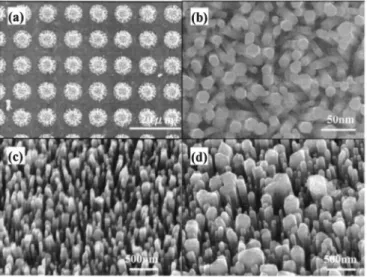
of ZnO nanorods was affected by the concentrations of the aqueous solution. Therefore, the same concentration of the precursors共0.01M兲 was used in this work to avoid the effect of solution concentration. Figure 2 shows the SEM images of the ZNs grown on the patterned ZnOf/ Si annealed at differ-ent temperatures, where the patterned ZnO film on Si sub-strate was fabricated by the photolithography and etching process. As the patterned ZnOf/ Si substrate was placed into the aqueous solution to grow ZNs, well-aligned ZNs are grown on the designed substrate, as shown in Fig. 2共a兲, and this demonstrates the selected growth behavior of the ZNs. Figure 2共b兲 shows the surface images of large-scale arrayed ZnO nanorods grown on the patterned ZnOf/ Si at room tem-perature, and the ZnO nanorods have a well-defined hexago-nal plane with a homogeneous diameter. Although the ZnOf/ Si substrate was patterned, nucleation of the nanorods was not correlated with the substrate patterning and subse-quent growth of the ZnO grains was also unaffected by pat-terning. However, as the patterned substrates were first an-nealed at 600 and 800 ° C, prior to the growth of the ZNs in the solution at 75 ° C, we found that the morphology of the ZNs was markedly changed, as shown in Figs. 2共c兲 and 2共d兲, especially for the ZnOf/ Si annealed at 800 ° C. Furthermore,
the dimension of ZNs increases with increasing annealing temperature. The average dimension of the ZNs is 20 and 300 nm in diameter for the ZnOf/ Si at room temperature and annealed at 800 ° C, respectively. When compared with the AFM images of ZnO film on Si substrate shown in Fig. 1, this seems to imply that the growth behavior of the ZNs is correlated with the grain size of the ZnO film sputtered on Si substrate, as illustrated in Fig. 3. Furthermore, there exists a critical temperature around 400 ° C, and above that, the ZNs are rapidly grown and become larger in diameter.
Figure 4共a兲 shows the TEM bright-field 共BF兲 image of the aligned ZNs grown on the annealed ZnOf/ Si substrate at 600 ° C. It was observed that most of the ZNs were grown along the direction perpendicular to the ZnOf/ Si substrate. The TEM dark-field image marked with arrows in the Fig. 4共b兲 reveals that there exists a close relationship between ZNs and ZnO film. Both ZNs and ZnOfon Si substrate were grown along the same direction of 关0002兴 and are coherent, as demonstrated by the selected-area electron diffraction
FIG. 1. AFM images of共a兲 as-grown ZnO films and 共b兲 annealed ZnO film
at 800 ° C.
FIG. 2. SEM images of the ZnO nanorods 共a兲 grown on the patterned
ZnOf/ Si, 共b兲 grown at room temperature, and grown on the annealed
ZnOf/ Si at共c兲 600 °C and 共d兲 800 °C.
FIG. 3. Both ZN diameter and ZnOf grain size as functions of annealing
temperature.
289 Hsiao et al.: Tunable growth of ZnO nanorods synthesized in aqueous solutions 289
共SAED兲 pattern 关inset of Fig. 4共b兲兴. In addition, as one ob-serves the interface between ZNs and ZnOf/ Si shown in Fig. 4共c兲, the high-resolution TEM 共HRTEM兲 image 关magnified from the marked area in Fig. 4共a兲兴 reveals that both the ZNs and ZnO films have identical parallel lattice fringes. This indicates that the ZNs seem to nucleate from the concave tip near the grain boundary共marked as lines兲 between two ZnO grains in ZnO films because it 共near the concave tip兲 has a higher surface energy. A detailed discussion can be referred to Ref. 5.
As the ZnOf/ Si substrate was annealed at a higher tem-perature of 800 ° C, a low-magnification TEM image of the ZNs was shown in Fig. 5共a兲. The HRTEM image of the ZNs marked with the box in Fig. 5共a兲 was further illustrated in
Fig. 5共b兲 where some nanorods are merged together to form a larger ZN along similar growth direction 关0002兴.8 The selected-area diffraction pattern共SADP兲 关shown in the inset of Fig. 5共b兲兴 reveals that the diffraction spots were split with several different angles. This suggests that the larger ZNs are not perfectly single crystalline and are consist of three ZNs, as illustrated in Figs. 5共c兲–5共e兲, with a slight misalignment between the nanorods. Therefore, the growth behavior of the larger ZnO nanorods can be considered from the direct com-bination of a small number of individual nanorods having a similar orientation.9
IV. CONCLUSIONS
We demonstrated that the growth of patterned ZnO nano-rods can be controlled by changing the annealing conditions of the ZnOf/ Si substrates. When the ZnOf/ Si substrate was annealed above a critical temperature to promote the crystal-lization of ZnO phase, both ZNs and ZnOf on Si substrate were found to become crystallographically matched. In this work, it reveals that the ZNs seem to preferentially nucleate from the cup tip near the grain boundary between two ZnO grains in the ZnO film. However, a higher annealing tem-perature may lead to the formation of a larger ZnO crystal due to coplanar coalescence behavior of several individual ZnO nanorods.
ACKNOWLEDGMENT
The authors gratefully acknowledge the financial support of the National Science Council of Taiwan through Contract No. NSC-93-2216-E-009-005.
FIG. 4. TEM共a兲 bright-field and 共b兲 dark-field images of the aligned ZNs
grown on ZnOf/ Si substrate annealed at 600 ° C. A corresponding
diffrac-tion pattern is shown in the inset of共b兲 for the selected single nanorod. 共c兲
A high-resolution TEM image of共a兲 showing the interface between ZNs and
ZnOf.
FIG. 5. 共a兲 Showing the low-magnification TEM images of ZnO nanorods
grown on the annealed ZnOf/ Si at 800 ° C.共b兲 HRTEM images of the ZnO
nanorods marked in the frame of共a兲 along with split diffraction pattern in
the inset. HRTEM image of the共c兲 left, 共d兲 middle, and 共e兲 right side of the
larger nanorod, showing that the larger ZnO nanorod seems to be composed of three ZNs.
This paper was presented at the First International Workshop on One Dimensional Materials, January 10–14, 2005, National Taiwan University, Taipei, Taiwan.
1D. P. Norton, Y. W. Heo, M. P. Ivill, K. Ip, S. J. Pearton, M. F. Chisholm,
and T. Steiner, Mater. Today 7, 34共2004兲.
2M. H. Huang, S. Mao, H. Feick, H. Yan, Y. Wu, H. Kind, E. Weber, R.
Russo, and P. Yang, Science 292, 1897共2001兲.
3W. I. Park, G.-C. Yi, M. Kim, and S. J. Pennycook, Adv. Mater.
共Wein-heim, Ger.兲 15, 526 共2003兲.
4J. H. Choy, E. S. Jang, J. H. Won, J. H. Chung, D. J. Jang, and Y. W. Kim,
Adv. Mater.共Weinheim, Ger.兲 15, 1911 共2003兲.
5S. C. Liou, C. S. Hsiao, and S. Y. Chen, J. Cryst. Growth 274, 438
共2005兲.
6L. Vayssieres and K. Keis, J. Phys. Chem. B 105, 3350共2001兲.
7C. C. Lin, C. S. Hsiao, S. Y. Chen, and S. Y. Cheng, J. Electrochem. Soc.
151, G285共2004兲.
8B. Liu and H. C. Zeng, J. Am. Chem. Soc. 125, 4430共2003兲.
9J. T. Sampanthar and H. C. Zeng, J. Am. Chem. Soc. 124, 6668共2002兲.
291 Hsiao et al.: Tunable growth of ZnO nanorods synthesized in aqueous solutions 291