國立交通大學
電子工程學系 電子研究所碩士班
碩 士 論 文
應用於無線感測網路之低功率 1.4-GHz
射頻前端接收器與傳送器電路設計
Low-Power 1.4-GHz Transceiver Front-End Circuit Design
for Wireless Sensor Network Application
研究生: 黃暉舜 (Hui-Shun Huang)
指導教授: 郭建男 博士 (Prof. Chien-Nan Kuo)
研究生: 黃暉舜 Student: Hui-Shun Huang
指導教授: 郭建男 教授 Advisor: Chien-Nan Kuo
國立交通大學
電子工程學系 電子研究所碩士班
碩士論文
A Thesis
Submitted to Department of Electronics of Engineering & Institute of Electronics College of Electrical Engineering and Computer Engineering
National Chiao Tung University In Partial Fulfillment of the Requirements
For the Degree of Master of Science
In
Electronic Engineering September 2011
Hsinchu, Taiwan, Republic of China
i 應用於無線感測網路之低功率 1.4-GHz 射頻前端接收器與傳送器電路設計 學生: 黃 暉 舜 指導教授: 郭 建 男 教授 國立交通大學 電子工程學系 電子研究所碩士班 摘要 本篇論文的主要目的在設計應用於無線感測網路之低功率射頻前端接收器 與傳送器電路。此接收器與傳送器被實現於一顆聯電 90 奈米 CMOS 製程的晶片 當中,整顆晶片的大小為 1360μm 1210μm。所設計之接收器為一組操作在 1.4-GHz 的低功率射頻前端接收電路,其包含有一顆低雜訊放大器、I/Q 降頻混 頻器以及一顆用以將此前後兩級交流耦合之變壓器。設計以共源級放大器串疊 架構來實現低雜訊放大器,適用於在低功率操作之下做高效率之訊號放大以及 電壓對電流之轉換。並且,設計三端變壓器將單端訊號轉換成為雙端訊號,進 一步地省去訊號轉換之功率消耗。最後,設計以雙平衡混頻器之架構來實現降 頻混頻器,把訊號降頻後再輸出。論文中針對變壓器的架構以及其共振操作加 以分析與設計,用以提供最大電流轉換增益。所設計之傳送器為一組操作在 1.4-GHz 的低功率射頻前端傳送電路,其包含有一顆升頻混頻器、一顆前級驅 動器以及一顆功率放大器。設計以被動架構來實現升頻混頻器,用以省去升頻 混頻器之功率消耗。並且,設計以反向器架構來實現前級驅動器,其適用於在 低功率操作之下對訊號的電壓擺幅做高效率的驅動。最後,設計以 A 類放大器 架構來實現功率放大器,用以完成高線性度的功率放大器。本論文將低雜訊放 大器之輸入阻抗匹配的電感和功率放大器之輸出阻抗匹配的電感整合於晶片當 中,進一步地在晶片上實現系統整合。此接收器與傳送器不只是針對低功率消 耗還設計其符合無線遠距醫療服務 Wireless Medical Telemetry Service (WMTS) 的 1.4-GHz 頻帶的各項規格。
ii
Low-Power 1.4-GHz Transceiver Front-End Circuit Design for Wireless Sensor Network Application
Student:Hui-Shun Huang Advisor:Prof. Chien-Nan Kuo Department of Electronic Engineering & Institute of Electronics
National Chiao-Tung University
ABSTRACT
This thesis aims to design a low-power 1.4-GHz transceiver front-end circuit for wireless sensor network application. The whole transceiver is implemented on a single chip by using UMC 90-nm CMOS technology, and the chip size is only 1360μm 1210μm. The designed receiver contains a low noise amplifier, I/Q down-conversion mixers, and a transformer which conducts AC coupling between the LNA and the mixers. The LNA is realized in the common-source cascode architecture which has high gain efficiency even in low-power operation. The 3-terminal transformer transfers the single-end signal to the differential form without power consumption. The I/Q down-conversion mixers are in the double-balance structure which is favorable for the direct-conversion receivers. This thesis focuses on the analysis of the transformer resonance operation for realizing the maximal current gain. The designed transmitter is composed of an up-conversion mixer, a pre-amplifier, and a power amplifier. The up-conversion mixer is realized in the passive architecture on the purpose of saving power consumption. The inverter-based pre-amplifier has efficient voltage gain with consuming a little DC current. The PA is realized by a class-A amplifier under the linearity consideration. The two inductances in the LNA input matching and the PA output matching are both integrated on this chip in order to achieve the sub-system integration. This transceiver is designed to not only reduce the power consumption but also meet all specifications of the 1.4-GHz band in Wireless Medical Telemetry Service.
iii
致謝
能完成此論文,首先得感謝我母親羅瑞玉女士和父親黃義昭先生的養育之 恩。感謝我母親多年來細心地照顧我的生活起居,不論是健康或是課業,母親 無微不至的照顧是我奮鬥課業最大的依靠。感謝我父親從我小時後就給我建立 積極正面的人生觀,讓我能勇敢地面對人生各種難題,每當我在成長的道路上 遇到阻礙時,父親不時的提點總是能讓我找到答案克服難題。 在交通大學碩士班的這兩年,首要感謝郭建男博士給我的指導和照顧。郭 教授不只是指導我設計射頻電路的技術,更讓我了解到做為一位理工領域學生 做研究應有的嚴謹態度。郭教授指導學生不遺餘力,當我的研究有困難時,郭 教授甚至是願意犧牲自己用餐的時間和我討論,我更是永遠無法忘記在我晶片 量測出狀況時,郭教授犧牲自己整天的假期,陪著我在實驗室裡一步一步地解 決問題。郭教授更是一位關心學生生活狀況的老師,不論是身體健康或是經濟 狀況郭教授都會不時給我最溫暖的問候。郭教授不只是我碩士班指導老師更是 我成長道路上的心靈導師,感謝郭教授總是在我對人生方向有所疑惑時給我建 議,每次的長談都讓我獲益良多。感謝郭教授在這兩年給我許多自由的空間, 在這兩年時間裡,不論是颱風天南下參與救災、學期中上山帶原住民小朋友功 課、暑假旅行上海以及去印度進行志工服務,老師總是鼓勵我勇往直前,把握 年輕時光體驗人生,讓我有精彩的碩士班生活。郭老師是位真正在乎學生的老 師,老師的對學生的批評與指教都是真正為學生好,感謝老師給予我的每一次 教誨,都提醒著我要更精進自己,不可鬆懈。郭老師的恩惠,終生難忘。 碩士班兩年,實驗室就像我第二個家。在此感謝俊興學長給我的指導與照 顧,俊興學長不只在課業和研究上給我許多的指導和幫助,更是給我許多面對 人生有用的建議。我永遠不會忘記俊興學長在數位通訊期末考前給我看他自己 整理的筆記,讓我順利通過考試。碩士班兩年,子超學長更是我親如手足的好 學長,子超學長不只教導我如何更有效率的做研究,更教我如何以更圓融態度iv 待人處世。我永遠忘不了當我的 VGA 設計有困難時,子超學長在一想到解決方 法時,當下就把點子告訴我,也協助我順利完成後續的設計。 感謝學長姐昶綜、鈞琳、明清、鴻源、燕霖、俊豪、建忠、冠豪、文彥、 勁夫、根生、博文和博一給我的指導與建議。感謝馳光學長給我雜訊量測的許 多協助和指導。也很開心認識第二年加入實驗室家愷和偉智。在此特別要感謝 敬修學長,敬修學長一步一步的帶領者我進行科專計畫,讓我後續接手能更得 心應手地應對。衷心感謝嘉佑和威震兩位學弟和我一起進行科專計畫,感謝兩 位學弟協助我多次地進行電路板的量測,感謝嘉佑學弟多次地協助我進行本篇 論文中的晶片的量測,你們真的辛苦了。感謝同學品全,總是願意在我研究或 是課業有問題時和我討論,並且給我許多有用的建議。感謝同學翰博,總是在 我有困難需要幫忙的時候兩肋插刀,我永遠不會忘記在我的 VGA 要量測時,翰 博多次協助並指導我下針量測的相關事項,我也永遠不會忘記在我和凱翔有困 難時,翰博毫不猶豫地借出八千元幫助我們。感謝同學豐榮在印刷電路板的 layout 部分給我許多有用的建議和幫忙,這也讓我更順利地執行科專計畫。 碩士班兩年多,最後要感謝我的好兄弟凱翔,不論是在課業、研究、生活、 感情、人生和家庭,真的很開心能夠在交大認識這一位無所不談、互相加油打 氣的好朋友,我永遠不會忘記在修習數位通訊時,凱翔多次特別為我補習,協 助我修得學分,碩士班兩年多來,大大小小各種困難,凱翔都給我許多幫助, 暉舜永遠銘記在心。 時光飛逝,轉眼間在風城已經六個寒暑,感謝老天爺指引我進入交通大學, 大學生活精彩充實,碩士班生活更是我人生的重要階段,這兩年多來的研究生 生活確實辛苦但也很紮實,著實讓我成長不少,讓我更有自信面對出社會後的 生活。還有太多需要感謝的人,無法一一答謝,請容暉舜在此一併感恩謝過。 黃暉舜 民國 100 年九月
v
Contents
Abstract (Chinese)………....i
Abstract (English)………ii
Acknowledgement………...iii
Table Captions………....vii
Figure Captions……….viii
Chapter 1 Introduction………....1
1.1 Wireless Sensor Network in Medical Application...………1
1.2 Literature Survey of Low-Power Transceiver………..2
1.3 Thesis Organization……….6
Chapter 2 System Application Scenario, Specification and
Structure………...7
2.1 System Application Scenario………...7
2.2 System Specification………..………..9
2.3 Proposed System Structure……….….………10
Chapter 3 Receiver Circuit Design………...12
3.1 Structure of the Low-Power 1.4-GHz Receiver……….12
3.2 Low Noise Amplifier……….…13
vi
3.4 Transformer Design………...17
3.5 Summary of the Receiver...………....23
Chapter 4 Transmitter Circuit Design……….26
4.1 Structure of the Low-Power 1.4-GHz Transmitter………..………..26
4.2 Up-Conversion Mixer………....27
4.3 Power Amplifier……….………....29
4.4 Pre-Amplifier……….35
4.5 Summary of the Transmitter………...………...37
Chapter 5 Chip Implementation and Measurements…….39
5.1 Chip Implementation……….…39
5.2 Chip Measurement………..………...41
5.3 Summary of the Measurement Results………..47
Chapter 6 Conclusion and Future Work……….49
6.1 Conclusion……….…49
6.2 Future Work……….………..50
Reference………....51
vii
Table Captions
Table 2.1 Transmitter specification……….…...10
Table 2.2 Receiver specification………...………..…………...10
Table 3.1 Transformer realization………..……22
Table 3.2 Summary of the simulated receiver performance……….…….25
Table 4.1 Summary of the simulated transmitter performance………..…....38
Table 5.1 Summary of the measured receiver performance………..……….45
Table 5.2 Summary of the measured transmitter performance…………..…………46
viii
Figure Captions
Fig. 1.1 Wireless body area network………..………..1
Fig. 1.2 Low-power 2.4-GHz direct-conversion (a) receiver (b) transmitter.………..2
Fig. 1.3 Low-power 868/915-MHz transceiver………...3
Fig. 1.4 Current reuse low power PA………...4
Fig. 1.5 Transformer based low power mixer………..4
Fig. 1.6 The proposed equivalent model of the transformer in reference [14]………5
Fig. 2.1 System application scenario of the wireless body area network……....……7
Fig. 2.2 Structure of the wireless sensor node……….………8
Fig. 2.3 RF transceiver front-end circuit blocks of the wireless sensor node………..9
Fig. 2.4 Proposed system structure of the low-power 1.4-GHz transceiver….…….10
Fig. 3.1 Schematic of the receiver core circuit……….……….12
Fig. 3.2 Smith chart of LNA input matching……….…13
Fig. 3.3 Receiver voltage conversion gain versus LO power…….………...16
Fig. 3.4 Block diagram of the receiver……….……….17
Fig. 3.5 (a) Designed 3-terminal transformer (b) Resonator coupling network...17
Fig. 3.6 Resonator coupling network………..………...18
Fig. 3.7 Two-port network of the RCN………..………19
ix
Fig. 3.9 Current gain contour plots mapping k and r (a) n=1(b) n=2(c) n=3(d) n=4.22
Fig. 3.10 Designed transformer………...…………..22
Fig. 3.11 Receiver schematic with C1 and C2………23
Fig. 3.12 Wireless sensor node and the power switch in the bias circuit…………...23
Fig. 3.13 Output buffer of the receiver………...………...…24
Fig. 3.14 Simulated receiver performance (a) Gain versus LO power (b) Frequency response………..24
Fig. 3.15 Simulated receiver performance (a) Noise figure (b) P1dB (c) IIP3 of I path (d) IIP3 of Q path………...25
Fig. 4.1 Schematic of transmitter core circuit………..………..26
Fig. 4.2 Passive CMOS SSB mixer……….………..28
Fig. 4.3 Conversion gain of the passive CMOS SSB mixer………..………29
Fig. 4.4 Signal conduction angle of class-A amplifier………..……….30
Fig. 4.5 I-V curve of 2.5-V RF nMOS (A) ID versus VGS, and (B) ID versus VDS...30
Fig. 4.6 (a) Maximum output power and power consumption versus VBias (b) Gain and efficiency versus VBias.……..………..……..32
Fig. 4.7 Output power matching of the PA……….………...33
Fig. 4.8 (a) Stability simulation setup of the PA without feedback network (b)Stability simulation setup of the PA with feedback network…..……...34
x
Fig. 4.9 Stability simulation results of PA
(a) Source stability circle and input impedance S11 of PA without feedback network (b) Load stability circle and output impedance S22 of PA without feedback network (c) Source stability circle and input impedance S11 of PA with feedback network (d) Load stability circle and output impedance S22 of PA with feedback network..34 Fig. 4.10 AC signal model of the pre-amplifier………..………...35 Fig. 4.11 Voltage gain and the power consumption of the pre-amplifier versus
the transistor size of Mn on the condition of =2/1…...……...36
Fig. 4.12 (a) PA power switch (b) Pre-amplifier power switch…………..………...37 Fig. 4.13 Simulated transmitter performance (a) Conversion gain
(b) Output power….………37 Fig. 5.1Inductance implemented in 3 metal layers………..……….……….39 Fig. 5.2 (a) Q factor of the inductances of 1, 2, and 3 metal layers (b) Noise figure of the receiver with the inductances of 1, 2, and 3 metal layers…….……...40 Fig. 5.3 Chip photo of the low-power 1.4-GHz transceiver………...………...40 Fig. 5.4 Measurement setups of the receiver for (a) Conversion gain (b) IIP3 by tone test (c) Noise figure………..………..41 Fig. 5.5 Laser burning………42 Fig. 5.6 The laser cut of C1’………...43
xi
Fig. 5.7 Peak shifts due to the laser cut of C1’………...43
Fig. 5.8 Measurement results of (a) Conversion gain versus LO power (b) Frequency response (c) Noise Figure (d) P1dB (e) IIP3_I (f) IIP3_Q…..……….44
Fig. 5.9 Measurement setup of the transmitter……...………...46 Fig. 5.10 Measurement results of the transmitter……….…….………46
1
Chapter 1 Introduction
1.1 Wireless Sensor Network in Medical Application
Recently, because the development of modern technology, the wireless sensor network (WSN) are widely used in medical service. In medical application, the WSN is usually employed in health monitoring. This WSN in medical application is called wireless body area network (WBAN), as shown in Fig. 1.1. A number of miniature sensor nodes are installed at human body and connected wirelessly together. The sensor nodes monitor the health conditions of human beings and communicate the biological signals to a center node by electrical signals. The center node collects all data and transmits it to other devices like cell phones by a telecommunication standard such as Wireless Local Area Network.
Hospitals and telemedical centers use the WBAN system to continuously monitor the health conditions of patients and conduct appropriate treatments earlier in emergencies. Because the sensor nodes of the WBAN are made in very small sizes and connected wirelessly together, patients would feel comfortable and their health conditions can be well controlled. To realize the miniature sensor nodes and
2
extend the lifetime of these devices with small batteries carried by patients, the circuits in the sensor nodes should be realized with high integration level, and the power consumption must be reduced.
1.2 Literature Survey of Low-Power Transceiver
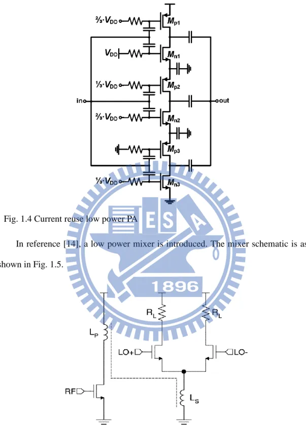
Using passive circuits, current reuse technique, and low supply voltage are three major way to reduce circuit power consumption. In this section, we introduce three low power circuits using these techniques.
In reference [11], a low-power 2.4-GHz direct-conversion RF transceiver is presented. The transceiver schematics are as shown in Fig. 1.3 (a) and (b).
(a)
(b)
3
The mixers in the transmitter and the receiver are both the passive CMOS mixer for saving power consumption. The driver amplifier of the transmitter is composed of two stages which are gain and out stages. The gain stage is the conventional cascode amplifier on the purpose of achieving high gain in low power operation. The folded-cascode architecture is employed in the output stage for higher voltage headroom under low supply voltage, thereby improving the linearity. The passive CMOS mixer is also employed in the transceiver in this thesis for saving power consumption.
In reference [13], a low-power 868/915-MHz transceiver for wireless sensor network is introduced. The transceiver block diagram is as shown in Fig. 1.3.
The most outstanding feature of this transceiver is the PA, as shown in Fig. 1.4. The author cascades three push-pull amplifiers at one current path. This current reuse architecture greatly enhances the PA efficiency. However, the PA output voltage swing is limited because the six cascode transistors. This current reuse architecture is only used in the low output power application.
4
In reference [14], a low power mixer is introduced. The mixer schematic is as shown in Fig. 1.5.
The transformer coupling effect is used between the transconductance stage and the switching stage of the mixer. The transformer based architecture reduces the supply voltage, and further saves the power consumption. The proposed equivalent model
Fig. 1.5 Transformer based low power mixer Fig. 1.4 Current reuse low power PA
5
of the transformer in reference [14] is as shown in Fig. 1.6.
The proposed equivalent model of the transformer in reference [14] is analyzed by the multivariate analysis. The multivariate analysis causes the difficulty to optimize the transformer.
The transformer technique is also used in the transceiver of this thesis for saving the power consumption. We propose a more efficient way to design an optimal transformer.
1.3 Thesis Organization
In Chapter 2, the system application scenario, specification and structure of the low-power 1.4-GHz transceiver are introduced, respectively. In Section 2.1, the system application scenario will be introduced. The system specifications of the transceiver are defined in Section 2.2. The proposed system structure for these specifications especially for low power consumption is presented in Section 2.3.
6
In Chapter 3, the designed structure of the low-power 1.4-GHz receiver and the circuit design of each block are introduced, respectively. Section 3.1 shows the designed structure of the receiver. A LNA in common-source cascade topology with inductive degeneration is introduced in Section 3.2. Section 3.3 presents the double balance down-conversion mixer. The analysis and design of the transformer resonant operation are introduced in Section 3.4. Section 3.5 gives a summary of the designed receiver.
In Chapter 4, the designed structure of the low-power 1.4-GHz transmitter and the circuit design of each block are introduced, respectively. Section 4.1 shows the designed structure of the transmitter. A passive up-conversion mixer is introduced in Section 4.2. Section 4.3 presents a class-A power amplifier. An inverter-based pre-amplifier is introduced in Section 4.4. Section 4.5 gives a summary of the design transmitter.
In Chapter 5, the chip implementation, measurement setups, and measurement results are introduced. Section 5.1 presents the chip implementation. The chip measurement setups and measurement results are putted in Section 5.2.
In Chapter 6, a conclusion and the future work are introduced. Section 6.1 gives a conclusion of this designed transceiver. Section 6.2 presents the future work of this topic.
7
Chapter 2
System Application Scenario, Specification and
Architecture
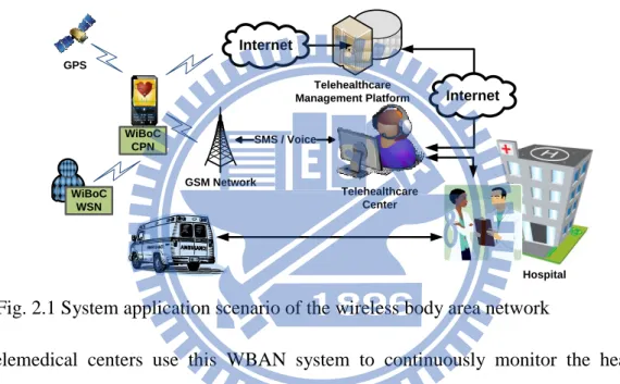
2.1 System Application Scenario
The system application scenario of the WBAN which this transceiver applies to is as showed in Fig. 2.1.
Telemedical centers use this WBAN system to continuously monitor the health condition of patients, especially disabled old persons. This WBAN are composed of wireless sensor nodes, electrocardiogram sensors (ECG sensors), cell phone system, and the expert system algorithm. The wireless sensor nodes are installed at the upper bodies of human beings. The sensor nodes sense the heartbeat, and communicate the electrocardiogram data to a center node by electrical signals. The center node collects all electrocardiogram data and updates it to telemedical centers through cell phone system. The expert system algorithm, which is installed in the cell phone, determines that the current electrocardiogram data is regular or not, and gives an alarm to telemedical centers or hospitals when the heat beat is not regular.
Fig. 2.1 System application scenario of the wireless body area network
Telehealthcare Management Platform Internet Hospital GSM Network SMS / Voice Telehealthcare Center GPS WiBoC CPN WiBoC WSN Internet
8
Telemedical centers use this system to continuously monitor the current electrocardiogram of patients and make appropriate medical treatments earlier for emergencies.
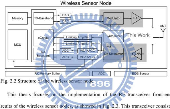
Fig. 2.2 shows the structure of the wireless sensor node this low-power transceiver applies to. The wireless sensor node is composed of an antenna, RF circuits, analog baseband circuits, digital baseband circuits, a micro controller unit (MCU), memories, and an ECG Sensor.
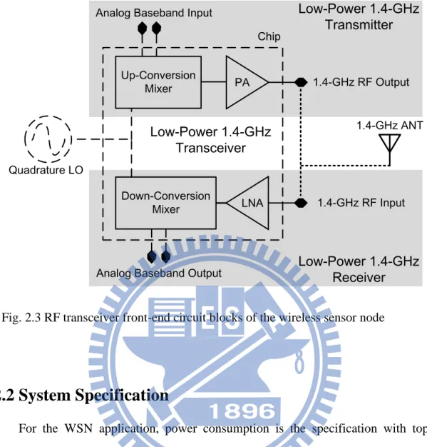
This thesis focuses on the implementation of the RF transceiver front-end circuits of the wireless sensor nodes, as showed in Fig. 2.3. This transceiver consists of an up-conversion mixer, a PA, a LNA, and I/Q down-conversion mixer. All circuits must be integrated and realized on a single chip of 90-nm CMOS process. All circuits except PA operate under 1-V VDD. In the transmitter, the up-conversion
mixer transfers the analog baseband signal to RF signal, and the PA provides the RF signal with power gain and outputs it to the antenna. In the receiver, the LNA amplifies the RF signal, and the I/Q down-conversion mixers transfer the RF signal to analog baseband signal. Both the transmitter and the receiver are direct-conversion structure. De-Modulator LNA Modulator PA ANT Synthesizer VGA+AGC VGA+AGC ADC ADC DAC DAC Limiting Amplifier Limiting Amplifier RX-Baseband TX-Baseband eCrystal MCU Memory
RX Memory Buffer ADC ECG Sensor
Wireless Sensor Node
This Work
9
2.2 System Specification
For the WSN application, power consumption is the specification with top priority. The power consumption specification of the transmitter and the receiver are 25-mW and 6-mW, respectively. The frequency channel is 1395-1400 MHz, which is one band of Wireless Medical Telemetry Service.
In this WBAN system application, the peak output power of the transmitter is 4-dBm, and the average output power of the transmitter is -3 dBm with 7 dB peak to average power ratio. According to the 4 dBm transmitter peak output power and 10% efficiency specification, the power consumption specification of the transmitter is 25-mW.
In this WBAN system application, the conversion gain specification of the receiver is 20 dB. System designer limits the receiver NF referred to the antenna
LNA Down-Conversion Mixer PA Up-Conversion Mixer Quadrature LO
Analog Baseband Input
1.4-GHz RF Output
Analog Baseband Output
1.4-GHz RF Input 1.4-GHz ANT Low-Power 1.4-GHz Transmitter Low-Power 1.4-GHz Receiver Chip Low-Power 1.4-GHz Transceiver
10
terminal to 7 dB with 6-mW power consumption. The linearity specification of the receiver is -25 dBm P1dB. Table 2.1 and Table 2.2 make the summary of the
specifications of the transmitter and the receiver, respectively.
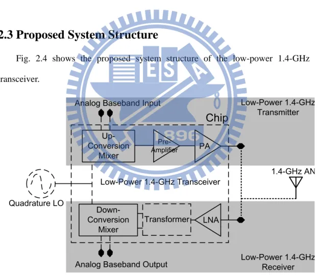
2.3 Proposed System Structure
Fig. 2.4 shows the proposed system structure of the low-power 1.4-GHz transceiver.
In this receiver, the first stage is a LNA which amplifies the 1.4-GHz RF signal and compresses noise of the receiver train, the second stage is a 3-terminal transformer as a passive balun which transfers the single-end signal to differential form without
LNA Down-Conversion Mixer PA Up-Conversion Mixer Pre-Amplifier Transformer Quadrature LO
Analog Baseband Input
Analog Baseband Output
Low-Power 1.4-GHz Transmitter Low-Power 1.4-GHz Receiver 1.4-GHz ANT
Chip
Low-Power 1.4-GHz TransceiverFig. 2.4 Proposed system structure of the low-power 1.4-GHz transceiver Table 2.1 Transmitter specification Table 2.2 Receiver specification
Peak Transmit Power 4 dBm Conversion Gain 20 dB Average Transmit Power -3 dBm Noise Figure 7 dB DC Power Consumption 25mW DC Power Consumption 6 mW
11
power consumption, and the final stage is I/Q down-conversion mixers which transfer the 1.4-GHz RF signal to the analog baseband signal with I/Q output. In the transmitter, the first stage is an up-conversion mixer which transfer the analog baseband signal to the 1.4-GHz RF signal, the second stage is a pre-amplifier which provides the RF signal with efficient voltage gain in order to give enough voltage signal swing to the PA stage, and the final stage is a PA, which provides the RF signal with power gain and outputs it to the antenna. Both the transmitter and the receiver take the off chip quadrature local oscillation (LO) signal source.
12
Chapter 3 Receiver Circuit Design
3.1 Structure of the Low-Power 1.4-GHz Receiver
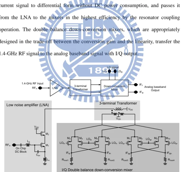
The designed structure of the low-power 1.4-GHz direct-conversion receiver is showed in Fig. 3.1, which is composed of a common source cascade LNA with inductive degeneration, a 3-terminal transformer as a passive balun, and I/Q double balance down-conversion mixers. The LNA completes both the input impedance matching and the noise matching at 1.4-GHz, amplifies the received RF signal and transfers it to current form. The 3-terminal transformer transfers the single-end RF current signal to differential form without DC power consumption, and passes it from the LNA to the mixers in the highest efficiency by the resonator coupling operation. The double balance down-conversion mixers, which are appropriately designed in the trade-off between the conversion gain and the linearity, transfer the 1.4-GHz RF signal to the analog baseband signal with I/Q output.
On Chip DC Block Lg Ls Cex VDD M1 M2 VDD VDD LOIp LOIn LOIn RIoad1 RIoad2 LOqp LOqn LOqn RIoad3 RIoad4 M3 IFIp IFIn IFQp IFQn M4 M5 M6 M7 M8 M9 M10
Low noise amplifier (LNA)
I/Q Double balance down-conversion mixer 3-terminal Transformer
LNA Transformer3-terminal Down-conversionMixer
1.4-GHz RF Input Analog baseband Output LO signal IFQ IFI LOI LOQ RFin RFin
13
3.2 Low Noise Amplifier
The first stage of the receiver is a common source cascode amplifier with inductive degeneration. This LNA is composed of a common source amplifier M1,
two inductances Lg and Ls, an external capacitor Cex, and a common gate amplifier
M2, as shown in Fig. 3-1. This type of amplifier has good gain efficiency which is an
appropriate choice for the low-power application. The source degeneration inductance Ls is in order to generate a real term in the input impedance of the LNA,
and we can choose appropriate value of Ls to generate a 50-Ω real term in the input
impedance. The gate inductance Lg is used to set the resonant frequency after Ls is
chosen in order to produce a pure 50-Ω input impedance matching in which the imaginary term is equal to zero. The external capacitor Cex is used to compensate the
small parasitic capacitor between gate and source of M1 in order to help Lg and Ls to
simultaneously complete the input impedance matching and the noise matching at 1.4-GHz. This type of input impedance matching is a narrow band input matching, as shown in Fig. 3.2. freq (500.0MHz to 2.000GHz) S (1 ,1 ) Readout M1 co nj( S op t) Readout M2 M1 indep(M1)= plot_vs(S(1,1), freq)=0.086 / -117.853 impedance = Z0 * (0.913 - j0.139) 1.400E9 M2 indep(M2)= plot_vs(conj(Sopt), freq)=0.106 / -12.166 impedance = Z0 * (1.231 - j0.056) 1.400E9 M1 & M2 @ 1.4 GHz
14
However, the wireless sensor network application is also a narrow band application. The operation frequency is from 1.395 to 1.400-GHz, so the narrow band input impedance matching is not a limitation. The common gate amplifier M2 provides
low impedance at the output node of common source amplifier M1, and leads to
negligible Miller effect of M1. M2 also provides high impedance at the output node
of M2 itself, which leads the LNA high gain in high frequency. Two inductances Lg
and Ls, and capacitor Cex complete both input impedance matching and noise
matching [6]. The input impedance and noise factor of this type of LNA can be expressed as: (3.1) (3.2)
where represents the parasitic capacitor between gate and source of M1, is
the transconductance of M1, is the series resistance of Lg, is the source
resistance, is a bias-dependent factor, is the zero-bias drain conductance of transistor M1. By eq. (3.1) and (3.2), we can design appropriate values of Vgs, Lg, Cex,
Ls, and the transistor sizes of M1 and M2 for specifications of the receiver. Here we
choose Vgs=0.43 V, Lg=7.6 nH with Q = 5.7, Cex=1.6 pF, Ls=0.7 nH,
,
and for the optimum noise matching and 50-Ω input impedance
matching in 4.5 mW DC power consumption. It can achieve simulated performance of -21.8 dB input insertion loss, 2.5 dB noise figure.
3.3 Down-Conversion Mixer Design
The third stage of the receiver is I/Q double balance down-conversion mixers. In the system application, the receiver has to have I/Q analog based band output, so the
15
I/Q double balance mixers are used here. The I/Q double balance mixers are composed of eight pMOS transistors M3-10 as the switching stage and four resistors
Rload1-4 as loads, as shown in Fig. 3-1. The double balance mixer has advantages of
better port-to-port isolation and less even-order distortion [2]. The letter is especially critical in the direct-down-conversion mixer.
A common mixer such as Gilbert Cell is composed of a transconductance stage, which transfers input RF voltage signal to current form, a current switching stage, which uses local oscillation signal to switching RF current signal and transfers it to analog baseband signal, and a load resistor stage. In this receiver, the LNA and the transconductance stage of mixers are combined together in order to save the DC power consumption of the transconductance stage of the mixers. The LNA amplifies the received RF signal and transfers the voltage signal to current form, and the 3-terminal transformer transfer the single-end RF current signal to differential form and passes it to the switching stage of the mixers. Finally, the current switching stage uses local oscillation signal to switch the RF current signal, and transfers it to the analog baseband signal.
pMOS transistors are employed in the switching stage of mixers, because pMOS transistor has better flicker noise performance as compare to nMOS transistor [6]. The ideal switching stage has that only one transistor of the switching pair is turned ON at the same time, and the current is equal to zero when the switch is turned OFF. Therefore, to make the switching stage more ideal, the transistors with bigger size are used, and the DC gate voltage bias is set to near threshold voltage. The load resistors are related to conversion gain and linearity of the mixers, as shown in Fig. 3.3.
16
In Fig. 3.3, the maximal conversion gain of the receiver is approximately proportional to the value of the load resistors. The bigger load resistors are used, the maximal conversion gain is higher, and the LO power of the maximal conversion gain is lower. However, the linearity of the receiver becomes worse with the increasing of the conversion gain. In the system application, there is a linearity specification of the receiver is -25 dBm P1dB. The appropriate value of the load resistors can be found by
trade-off between the linearity and the conversion gain of the receiver.
In the design of the mixers, each value of each component can be defined by following above design considerations. The transistor sizes of M3-10 is
, the DC gate voltage bias of the switching stage is 0.2-V VSG, and the load
resistors Rload1-4 are 800 Ω. The total DC power consumption of two double balance
mixers is 0.5-mW. The LO power of maximal conversion of the designed receiver is -5 dBm, which is lower than the LO power of the common receivers.
-15 -12 -9 -6 -3 0 3 4 8 12 16 20 24 R e c e iv e r V o lt a g e C o n v e rs io n G a in ( d B ) LO Power (dBm) RIoad=1600 Ω RIoad=1200 Ω RIoad=800 Ω RIoad=400 Ω
17
3.4 Transformer Design
Between the LNA and the mixers, there is a 3-terminal transformer, as shown in Fig. 3.4. The 3-terminal transformer needs to be carefully designed to transfer the single-end RF current signal to differential form with the maximal current gain.
The 3-terminal transformer is composed of two coupled resonators, which is called resonator coupling network (RCN). Under the critical resonance condition, the RCN can provide the maximal current gain at resonance frequency, which is almost equivalent to an ideal transformer [6]. Fig. 3.5 (a) shows the transformer used in the receiver. It can be modeled into the resonator coupling network, as shown Fig. 3.5 (b).
In Fig. 3.5 (b), L1 is the primary coil of the transformer, L2 and L3 are two secondary
coils of the transformer with the same value, and M is the mutual inductance between primary and secondary coils. C1 and L1 form a resonator which connects to the output
node of the LNA, and L2, C2, L3, and C3 form two resonators which connect to the L2 L3 C2 C3 L1 C1 M M (a) (b) Transformer
Fig. 3.5 (a) Designed 3-terminal transformer, (b) Resonator coupling network
LNA Down-conversionMixer
1.4-GHz RF Input Analog baseband output LO signal IFQ IFI LOI LOQ RFin 3-terminal Transformer
18
input nodes of the mixers. The whole receiver is modeled into the equivalent network, as shown in Fig. 3.6. In Fig. 3.6, RLNA and CLNA model the output impedance of the
LNA, L1 and Cp1 model the inductance and parasitic capacitor of the primary coil of
the transformer, L2-3 and Cp2-p3 model the inductances and parasitic capacitors of the
secondary coils of the transformer, and CMixer1-4 and RMixer1-4 model the input
impedance of the mixers. The two parallel capacitors CLNA and Cp1 form the C1 of the
RCN, and Cp2-p3 and CMixer1-4 form the C2 of the RCN.
The transformer connects two identical parallel double balance mixers, so these two mixers can be basically simplified into a mixer with double size. Moreover, because the transformer is symmetric to the virtual ground of secondary coil, the RCN can be analyzed by the two-port network, as shown in Fig. 3.7. Iin represents the RF current
signal from the LNA, C1 includes the parasitic capacitors of the LNA and the primary
coil of the transformer and C2 includes the parasitic capacitors of the mixers and the
secondary coils of the transformer.
CLNA Cp1 L1 RLNA CMixer3 Cp2 L2 CMixer4 Cp3 L3 CMixer1 RMixer1 CMixer2 RMixer3 RMixer2 RMixer4 Equivalent model of the LNA Equivalent model of the Mixers Equivalent model of the
3-end transformer
C1
C2
19
The resonance frequencies of primary and secondary uncoupled resonators are defined as ω1 and ω2, and m is the ratio of these two resonance frequencies.
(3.3)
The mutual inductance between the primary and secondary coils is M, and the coupling coefficient is defined as
k
(3.4) In the coupled network, the resonance frequencies would shift to other two frequencies, as shown in Fig. 3.8. These two resonance frequencies in coupled network can be expressed in term of m, k, and ω2, as shown in eq. (3.5) and (3.6) [6].
(3.5)
(3.6) At these two resonance frequencies ωH and ωL, the transformer passes the RF current
signal from the LNA to the mixers in highest efficiency. Either resonance frequency can be chosen as the operating frequency.
ω
1ω
2ω
Lω
HFig. 3.8 Resonance frequencies of the RCN
C
1L
1-M L
2-M
R
LNAI
inM
C
2RMixer
Z
in1Z
in2Z
in3I
out20
In the two-port analysis, the transfer function from Iin to Iout at the resonance
frequency is derived as
where
(3.7) The k is the coupling coefficient between the primary coil and the secondary coils, and n is the ratio of the inductance of the primary coil to the inductance of one secondary coil. The k and n of the maximal current gain condition can be found by the partial differential equation of eq. (3.7) for k and n. These two partial differential equations are (3.8)
These two partial differential equations lead the result as
(3.9)
Eq. (3.9) means the impedance matching between the LNA and the transformer. The impedance matching also happens at the interface between the transformer and the mixers. Under the critical coupling condition, the RF current signal is coupled from the LNA to the mixer in the highest efficiency. From eq. (3.7) and (3.9), the maximal current gain under the critical coupling condition is
(3.10)
Eq. (3.10) means that the maximal current gain of the transformer is determined by
and . The RCN gets the same result of the maximal current gain like an
ideal transformer as k and n are chosen appropriately. eq. (3.10) also means that the maximal current gain is higher with higher RLNA and lower RMixer. This result
21
low impedance. With the same voltage drop between the high impedance node and the low impedance node, more current is injected when the high-impedance is higher and the low-impedance is lower.
The higher impedance ratio of RLNA/RMixer is design to get the higher maximal
current gain under the critical coupling condition. Under the condition of that all performances of the receiver meet all specifications, the output impedance of the LNA and the input impedance of the mixer are designed to as higher and as lower as possible, respectively. In this receiver, is designed to be 552 Ω and is designed to be 15 Ω. Therefore, maximal current gain
is equal to
about 3. After getting the value of maximal current gain of the RCN, the corresponding ratio of and the ratio of need to be chosen to realize the transformer with the maximal current gain at 1.4 GHz. In the current gain contour plots mapping k and r of n=1~4, as shown in Fig. 3.8, there are two areas of maximal current gain when and in each contour plot, that represents two resonance frequencies of the RCN ωH and ωL. The maximal current gain of
operates at ωH and the other one operates at ωL. The area of the maximal current gain
at ωL is bigger than the other one at ωH, so the RCN is designed at ωL can be more
tolerant of the variation of r and k. Therefore, the RCN at ωL is easier to be realized
22
Here, n is chosen as 3. In Fig. 3.9 (c), the current gain degrades very little when k ranges from 0.4 to 0.6. The designed transformer is as shown in Fig. 3.10, in which W1 = 8 μm, W2 = 10 μm, OD = 400 μm. Table 3.1 shows each parameter of the RCN.
Because the designed RCN needs bigger capacitances C1 and C2 which are
bigger than the total capacitance of the parasitic capacitances of the LNA and primary coils of the transformer and the parasitic capacitance of the secondary coils of the transformer and the mixers. Therefore, there are two additional capacitors C1’ and C2’
Table 3.1 The RCN realization
OD W
2
W1
Fig. 3.10 Designed transformer
L1 11.53 nH L2 1.79 nH C1 0.35 pF C2 3.3 pF n 2.54 k 0.55 k r n=2 2.96 2.6352.31 2.96 2.63 5 2.31 0 0.2 0.4 0.6 0.8 1 0.5 1 1.5 2 2.5 3 0.5 1 1.5 2 2.5 k r n=1 2 .9 6 2.6352.31 2.96 2.63 5 2.31 0 0.2 0.4 0.6 0.8 1 0.5 1 1.5 2 2.5 3 0.5 1 1.5 2 2.5 k r n=3 2.96 2.635 2.31 2.96 2.635 2.31 0 0.2 0.4 0.6 0.8 1 0.5 1 1.5 2 2.5 3 0.5 1 1.5 2 2.5 k r n=4 2.96 2.635 2.31 2.96 2.63 5 2.31 0 0.2 0.4 0.6 0.8 1 0.5 1 1.5 2 2.5 3 0.5 1 1.5 2 2.5 (a) (b) (c) (d)
23
putted between the LNA and the transformer and between the transformer and the mixers in order to compensate the parasitic capacitances to realize the needed C1 and
C2, as shown in Fig. 3.11.
3.5 Summary of the Receiver
The low-power 1.4-GHz receiver can be realized by following the design procedure in Section 3.1, 3.2, and 3.3. Moreover, there is a micro control unit (MCU) in each wireless sensor node which would switch all active circuits ON/OFF by digital signal Vc, as shown in Fig. 3.12. This power switch function can save more power consumption by tuning active circuits OFF when they are not needed. Therefore, there are power switches in the bias circuits of all active circuits which can switch the active circuits by changing the bias, as shown in Fig. 3.12.
De-Modulator LNA Modulator PA ANT Synthesizer VGA+AGC VGA+AGC ADC ADC DAC DAC Limiting Amplifier Limiting Amplifier RX-Baseband TX-Baseband eCrystal MCU Memory
RX Memory Buffer ADC ECG Sensor
Wireless Sensor Node
This Work
VDD
Bias Circuit
VC
Fig. 3.12 Wireless sensor node and the power switch in the bias circuit
On Chip DC Block Lg Ls Cex VDD M1 M2 VDD VDD LOIp LOIn LOIn RIoad1 RIoad2 LOqp LOqn LOqn RIoad3 RIoad4 M3 IFIp IFIn IFQp IFQn M4 M5 M6 M7 M8 M9 M10 RFin C2' C2' C1'
24
After the mixers, there are source follower output buffers, as shown in Fig. 3.13. The output buffers are for the output 50-Ω impedance matching under measurement consideration. The gain of the output buffer is about 8.4 dB in simulation when the loads are 50-Ω resistors.
The receiver can achieve the simulated performance of 27.7 dB conversion gain before buffer, 19.3 dB conversion gain after buffer, -21 dBm P1dB, -13 dBm IIP3, and
3.1 dB noise figure, as shown in Fig. 3.14 and Fig. 3.15. The DC power consumption of the whole receiver is 6 mW. Table 3.2 makes the summary of all simulated performance and the specifications of the receiver.
-15.0 -12.5 -10.0 -7.54 -5.0 -2.5 0.0 2.5 5.0 8 12 16 20 24 28 32 R e c e iv e r C o n v e rs io n G a in ( d B ) LO Power (dBm) 1.0 1.1 1.2 1.3 1.4 1.5 1.6 1.7 1.8 1.9 2.0 8 12 16 20 24 28 32 R e c e iv e r C o n v e rs io n G a in ( d B ) RF Frequency (GHz) (a) (b)
Sim I (before buffer)
Sim Q (before buffer)
Sim I (after buffer)
Sim Q (after buffer)
Sim I (before buffer)
Sim Q (before buffer)
Sim I (after buffer)
Sim Q (after buffer)
Fig. 3.14 Simulated receiver performance (a) Gain versus LO power (b) Frequency response
LNA Transformer Down-conversion Mixer
I/Q LO Signal RF Input Buffer Output Buffer Mixer Output IF I/Q Output 50 Ω Mixer VDD Off-chip DC block
25
Table 3.2 Summary of the simulated receiver performance
Path I Path Q Specification Conversion Gain 27.7 dB 27.8 dB 20 dB
P1dB -21 dBm -23 dBm -25 dBm
IIP3 -13 dBm -14.5 dBm N/A
Noise Figure 3.1 dB 3.1 dB 7 dB Power Consumption Total power consumption = 6 mW 6 mW
-50 -45 -40 -35 -30 -25 -20 -15 -10 4 8 12 16 20 24 28 32 R e c e iv e r C o n v e rs io n G a in ( d B ) RF Power (dBm) 1.0 1.2 1.4 1.6 1.8 2.0 2 3 4 5 6 7 N o is e F ig u re ( d B ) RF Frequency (GHz) (a) (b) (c) (d) 1dB -50 -45 -40 -35 -30 -25 -20 -15 -10 -120 -100 -80 -60 -40 -20 0 20 O u tp u t P o w e r (d B m ) Input RF Power (dBm) -50 -45 -40 -35 -30 -25 -20 -15 -10 -120 -100 -80 -60 -40 -20 0 20 O u tp u t P o w e r (d B m ) Input RF Power (dBm) Sim Q Sim I Sim IF I Sim IF Q Sim 3rd I Sim 3rd Q 1dB
Sim I (before buffer)
Sim Q (before buffer)
Sim I (after buffer)
Sim Q (after buffer)
Fig. 3.15 Simulated receiver performance (a) Noise figure (b) P1dB (c) IIP3 of I
26
Chapter 4 Transmitter Circuit Design
4.1 Structure of the Low-Power 1.4-GHz Transmitter
The designed structure of the 1.4-GHz low-power direct-conversion transmitter is showed in Fig. 4.1, which is composed of a passive CMOS up-conversion mixer, an inverter-based pre-amplifier, and a class-A power amplifier (PA) with resistor feedback network.
The passive CMOS up-conversion mixer transfers the analog baseband signal to 1.4-GHz RF signal without DC power consumption. The dummy transistor
Mdummy is used to make mixer operate more symmetrically. The inverter-based
pre-amplifier amplifies the RF voltage signal and provides sufficient voltage signal swing to PA. The class-A power amplifier with resistor feedback network provides
LOIn LOIn LOIp LOIp IFIp IFIn LOQn LOQn LOQp LOQp IFQn IFQp MN MP MPA Cf Rf LD CD 50 Ω Load VC M2 M4 M1 M3 M6 M8 M5 M7 Mdummy C1 C2 1V VDD 1.7V VDD RX
Passive CMOS up-conversion mixer
Pre-amplifier PA PA Up-conversion mixer Pre-amplifier
Analog baseband input
RFoutput LO Signal RFoutput IFI IFQ LOI LOQ 1.4-GHz RF output Mswitch
27
the RF signal with power gain and outputs it to a 50-Ω load. The on-chip inductance LD is used as a RF choke, CD completes output power matching of the PA, and Rf
and Cf form a feedback network for stability consideration. C1 and C2 are on chip
DC blocks.
4.2 Up-conversion Mixer Design
The first stage of the low-power 1.4-GHz transmitter is a passive CMOS up-conversion mixer. The passive mixer is composed of eight transistors M1~8, as
shown in Fig. 4.1. This mixer modulates the QPSK analog baseband signal to 1.4-GHz RF signal, and suppresses the LO leakage. In order to reduce DC power consumption of the transmitter and put more budget of power consumption into the PA stage for achieving higher signal output power, the passive mixer is employed. In the implementation, CMOS technology is chosen to realize the passive mixer, because of its good switching property [16]. The nMOS transistor is used to realize the passive CMOS mixer, because that nMOS transistor has better switching performance due to the higher mobility of electrons than holes. The up-conversion mixer is composed of two double balance mixers, as shown in Fig. 4.3, so this mixer naturally has the advantages of double balance mixer. The double balance mixers provides good LO leakage suppression, because the good port-to-port isolation.
28
In this transmitter, there is no differential-to-single-end circuit between the mixer and the pre-amplifier for saving power consumption. One path of the mixer differential output is connected to the pre-amplifier, and the other one path is terminal to the dummy transistor Mdummy. The transistor size of Mdummy is designed
to create the similar impedance looking into the pre-amplifier in order to balance the differential output load of the mixer. The mixer operates more symmetrically, the better LO leakage and RF image rejections would be obtained.
The conversion gain and linearity are two critical points which should be considered in the mixer design. Fig. 4.3 shows that the conversion gain of the passive mixer is higher when the bigger switching size is used, but its linearity is worse in the same case. Therefore, there is a trade-off between conversion gain and linearity in the mixer design. The size of the passive CMOS mixer is chosen as 16μm/0.09μm in consideration of both conversion gain and linearity. This mixer achieves the performances of conversion gain Amixer = -6.5 dB, and linearity IP1dB =
0 dBm. LOIp LOIp LOIn LOIn IFIp IFIn LOQp LOQp LOQn LOQn IFQn IFQp M1 M2 M3 M4 M5 M6 M7 M8 RF+ RF
-Double balance mixer I Double balance mixer Q
29
4.3 Power Amplifier
The output stage of the low-power 1.4-GHz transmitter is a class-A power amplifier (PA) with resistor feedback network. The PA is composed of MPA, LD, CD,
Rf, and Cf, as shown in Fig. 4.1. The on chip inductance LD is used as a RF choke,
CD completes output power matching of the PA, and Rf and Cf form a feedback
network for stability consideration. The peak transmit power of the transmitter is 4 dBm, so a high linear PA is needed here. In this transmitter design, a class-A amplifier is employed in the PA stage due to the advantage of high linearity [7], which is critical for this work. The power consumption and the efficiency are other two specifications the transmitter must meet. The maximal total power consumption of the transmitter is 25 mW, and the efficiencyη which is defined in eq. (4.1) of the transmitter must be higher than 10%.
η (4.1) The class-A amplifier is biased in the condition of that the transistor is always
-20 -16 -12 -8 -4 0 4 -12 -10 -8 -6 -4 -2 M ix e r c o n v e rs io n g a in ( d B ) Input IF power (dBm) Mixer size = 8 μm / 90 nm Mixer size = 16 μm / 90 nm Mixer size = 24 μm / 90 nm Mixer size = 32 μm / 90 nm
30
ON and it always conducts the quiescent current. The signal conduction angle of class-A amplifier is 360o, as shown in Fig. 4.4.
There are two types of RF transistors in UMC CMOS 90-nm technology, which are 1-V RF MOS and 2.5-V RF MOS. Under the same current bias condition, 1-V RF MOS has higher transconductance than 2.5-V RF MOS has, but 2.5-V RF MOS has higher linearity than 1-V RF MOS has. For the linearity consideration, the 2.5-V RF nMOS is employed to realize the PA stage. Fig. 4.5 (A) and (B) show the I-V curve of the 2.5-V RF nMOS .
Fig. 4.5 (a) shows ID-VGS curve of the 2.5-V RF nMOS. In the real design
environment, there is no specific corner point of the threshold voltage Vt in the
ID-VGS curves. Here we define that the corner point is located at the cross point of
the extended tangent lines of the pinch-off region and the saturation region. Vt can 0.0 0.5 1.0 1.5 2.0 2.5 3.0 3.5 4.0 0 15 30 45 60 75 90 ID ( m A ) V DS (V) Vt = 0.7 V 0.0 0.2 0.4 0.6 0.8 1.0 1.2 1.4 1.6 0 10 20 30 40 50 60 ID ( m A ) V GS (V) Load Line Vmin VDC VMax Imin Imax VGS = 1.5 V VGS = 1.3 V VGS = 1.1 V VGS = 0.9 V VGS = 0.7 V VGS,max VGS,min IDC (a) (b)
Fig. 4.5 I-V curve of 2.5-V RF nMOS (A) ID versus VGS, and (B) ID versus VDS
VBias Vt 0 π 2π 3π 4π Vin (V) Iquiescent Ipeak 0 π 2π 3π 4π ID (A )
Angular time Angular time
31
be figured out by the above definition, and its value is 0.7 V. Therefore, the gate voltage bias VBias of the class-A PA must be higher than 0.7 V for the 360o signal
conduction angle. Fig. 4.5 (b) shows the ID-VDS curve of the 2.5-V RF nMOS, and
the load line analysis. A linear amplifier always operates in the saturation region which is between the triode region and the breakdown region. In the load line analysis, Vmin, which is defined as Vmin = VGS - Vt, is the lowest output voltage. The
corresponding current of Vmin is the maximum output current Imax. The breakdown
voltage of the 2.5-V RF MOS is very high when VGS is low. ID increases very slowly
as VGS = 0.7 V, as shown in Fig. 4.5 (b), so the transistor breakdown is not the
limitation of linearity. Here we define that Vmax is the VDS with 1 dB increasing of ID
in the saturation region as VGS = Vt = 0.7 V, its value is equal to 2.8 V. The
corresponding current of Vmax is the minimum output current Imin. From the above
definition, the maximum output power of the trasistor can be expressed as
(4.2)
By eq. (4.2), the maximum output power in different cases can be obtain. For example, the output voltage is from 0.9 V to 2.8 V as input voltage Vin is from 1.6 V
to 0.7 V, as shown in Fig. 4.5 (b). The corresponding Imax and Imin are 57.9 mA and
3.1 mA, respectively. Therefore, the maximum output power
is . The corresponding gate
voltage bias VBias is
, and VDS is
. Under this bias condition, the DC current ID can found out in Fig. 4.5 (a), and ID in this case is
26.67 mA. The RF choke used in the PA is a 9.5-nH inductance, and its parasitic resistor is 6 Ω. Therefore, the appropriate VDD is
32
. The efficiency of the PA is η
. Fig. 4.6 (a) and (b) make the summaries of the maximum output power, the DC power consumption, the power gain, the efficiency of the PA as VBias is from
0.75 V to 1.15 V.
Fig. 4.6 (a) and (b) show that the maximum output power is higher with higher DC power consumption. However, the maximum output power is not proportional to the DC power consumption. With VBias increasing, the growth rate of power
consumption increases, but the growth rate of the maximum output power decreases. Therefore, there is a VBias of the highest efficiency can be obtained, as shown in Fig.
4.6 (b). The VBias of the highest efficiency is 0.95 V and the efficiency changes
slowly as VBias is from 0.9 V to 1.0 V. The corresponding VDD of the VBias in this
range is from 1.67 V to 1.8 V, and the same bias condition of high efficiency would be obtained in the different transistor sizes. In this work, the VBias is chosen to be
0.92 V, the corresponding VDD is 1.7, and the transistor size is 288μm/0.36μm. This
PA can achieve the simulated performance of OP1dB = 6 dBm and 19.2% efficiency
with 20.7 mW power consumption.
Fig. 4.7 shows the output power matching by Smith chart in the simulation. S11
0.7 0.8 0.9 1.0 1.1 1.2 0 5 10 15 20 25 30 35 P A E ff ic ie n c y ( % ) VBias (V) 0.7 0.8 0.9 1.0 1.1 1.2 -15 -10 -5 0 5 10 15 V Bias (V) M a x im a l O u tp u t P o w e r (d B m ) 0 10 20 30 40 50 60 P o w e r C o n s u m p tio n ( m W )
Fig. 4.6 (a) Maximum output power and power consumption versus VBias (b) Gain
33
is the output impedance, and maker M1 marks the impedance at 1.4 GHz, which is . S22 is the impedance looking into the matching network, and maker M2 marks the impedance at 1.4 GHz, which is . The value of CD is chosen to be 1.8 pF to achieve the output impedance matching.
Rf and Cf form a feedback network for stability consideration. Fig. 4.9 (a), (b),
(c), and (d) are the stability simulation results of PA by the simulation setup in Fig. 4.8 (a) and (b). Fig. 4.9 (a) shows the source stability circle and input return loss S11 of PA without feedback network. Fig. 4.9 (c) shows the load stability circle and output return loss S22 of PA without feedback network. In Fig. 4.9, the areas inside the blue circles and outside the red circles are the areas of stable input and output impedance at each frequency. The input and output impedance of the PA should be designed in the stable impedance area. In Fig. 4.9 (a), the input impedance points are near the unstable area. In Fig. 4.9 (c), some output impedance points are in the unstable area. Rf = 2.5 kΩ and Cf = 2.7 pF are used to complete the feedback
network to solve the stability issue, as shown in Fig. 4.8 (b). Fig. 4.9 (b) and (d) show the simulation results of stability of the PA with the feedback network. In Fig. 4.9 (b), the input impedance points shift a little bit away from the unstable area. In Fig. 4.9 (d), all output impedance points are in the stable impedance area.
MPA Cf Rf LD CD 50 Ω Load C2 1.7V VDD S11S22 freq (500.0MHz to 3.000GHz) S (1 ,1 ) Readout M1 S (2 ,2 ) Readout M2 M2 freq= S(2,2)=0.510 / -58.340 impedance = 51.051 - j59.892 1.400GHz M1 freq= S(1,1)=0.481 / 55.212 impedance = Z0 * (1.127 + j1.157) 1.400GHz M1 & M2 @ 1.4 GHz
34 indep(S_StabCircle1) (0.000 to 51.000) S_ St a b C irc le 1 freq (8.500GHz to 14.00GHz) S(1 ,1 ) indep(S_StabCircle1) (0.000 to 51.000) S_ St a b C irc le 1 freq (8.000GHz to 14.00GHz) S(1 ,1 ) (a) (b) indep(L_StabCircle1) (0.000 to 51.000) L _ St a b C irc le 1 indep(L_StabCircle1) (0.000 to 51.000) L _ St a b C irc le 1 freq (100.0MHz to 14.00GHz) S(2 ,2 ) (c) (d) freq (100.0MHz to 14.00GHz) S(2 ,2 ) indep(S_StabCircle1) (0.000 to 51.000) S_ St a b C irc le 1 freq (100.0MHz to 7.500GHz) S(1 ,1 ) freq (100.0MHz to 14.00GHz) St a b M e a s1 St a b M e a s1 S(1 ,1 ) indep(S_StabCircle1) (0.000 to 51.000) S_ St a b C irc le 1 freq (100.0MHz to 7.500GHz) S(1 ,1 ) freq (100.0MHz to 14.00GHz) St a b M e a s1 St a b M e a s1 S(1 ,1 ) indep(L_StabCircle1) (0.000 to 51.000) L _ St a b C irc le 1 L _ St a b C irc le 1 freq (100.0MHz to 14.00GHz) S(2 ,2 ) indep(L_StabCircle1) (0.000 to 51.000) L _ St a b C irc le 1 indep(L_StabCircle1) (0.000 to 51.000) L _ St a b C irc le 1 indep(L_StabCircle1) (0.000 to 51.000) L _ St a b C irc le 1 L _ St a b C irc le 1 freq (100.0MHz to 14.00GHz) S(2 ,2 )
Fig. 4.9 Stability simulation results of PA
(a) Source stability circle and input impedance S11 of PA without feedback network (b) Load stability circle and output impedance S22 of PA without feedback network (c) Source stability circle and input impedance S11 of PA with feedback network (d) Load stability circle and output impedance S22 of PA with feedback network
MPA Cf Rf LD CD 50 Ω 1.7V VDD 50 Ω S11 S22 MPA LD CD 50 Ω 1.7V VDD 50 Ω S11 S22 C2 C2 (a) (b)
Fig. 4.8 (a) Stability simulation setup of the PA without feedback network (b) Stability simulation setup of the PA with feedback network
35
4.4 Pre-Amplifier
There is an inverter-based pre-amplifier between the up-conversion mixer and the power amplifier. The pre-amplifier is composed of a pMOS common source amplifier MP, a nMOS common source amplifier MN, a power switch Mswitch, and a
resistor RX, as shown in Fig. 4.1. The pre-amplifier is used to amplify the voltage
swing of the RF signal and provides sufficient signal voltage to the PA. These two common source amplifiers share one DC current path, and the pre-amplifier is self-biased with the 12.5-kΩ resistor RX. Fig. 4.10 shows the AC signal model of the
pre-amplifier.
The and are the transconductance of Mp and Mn, and
r
op andr
on are theoutput resistance of Mp and Mn. The voltage gain of the pre-amplifier is
(4.3)
This type of amplifier has two transconductance gains with one current path, so it can provides signal with efficient voltage gain in low power operation [5]. The DC voltages at Vout and Vin are self biased at VDD/2 for maximum voltage swing.
The mobility ratio of the 1-V RF pMOS to 1-V RF nMOS in UMC 90-nm is about 1:2. Therefore, the transistor size ratio of is chosen as 2/1 to
g
mnV
gsng
mpV
gspr
op// r
onV
outV
inV
gsnV
gsp36
bias the DC voltages at Vout and Vin to VDD/2. The input voltage swing of the PA is
0.26 V as its output power reach OP1dB. Therefore, the pre-amplifier must has
efficient voltage gain to provide sufficient voltage to the PA. The power consumption budget of the whole transmitter is 25 mW and the PA consumes 20.7 mW, so the leaved remained power consumption budget for the pre-amplifier is 4.3 mW. Fig. 4.11 shows the voltage gain and the power consumption of the pre-amplifier versus the transistor size of Mn with =2/1. Both Lp and
Ln always keep the smallest size of 90 nm for maximal voltage gain.
In this work, the transistor sizes of the pre-amplifier are and for optimal voltage self bias at VDD/2. This pre-amplifier
achieves the performances of voltage gain with 3.9 mW DC power consumption. The transistor Mswitch is a DC power switch to control
ON/OFF for saving the power consumption.
10 20 30 40 50 60 70 80 -8 -4 0 4 8 12 16 20 W n (m) V o lt a g e G a in o f P re -A m p li fi e r (d B ) 0 1 2 3 4 5 6 7 P o w e r C o n s u m p ti o n o f P re -A m p li fi e r (m W ) Voltage gain Power consumption
Fig. 4.11 Voltage gain and the power consumption of the pre-amplifier versus the transistor size of Mn on the condition of =2/1

![Fig. 1.6 The proposed equivalent model of the transformer in reference [14]](https://thumb-ap.123doks.com/thumbv2/9libinfo/8469092.183458/18.892.137.748.167.761/fig-proposed-equivalent-model-transformer-reference.webp)