無電鍍沉積二氧化釕與釕複合薄膜之特性研究
學生:陳境妤 指導教授:吳樸偉 博士
國立交通大學材料科學與工程學系
摘要
35–300 nm 非晶形二氧化釕及釕之複合薄膜已成功地以一新開發
的鍍液配方,用無電鍍沉積的方式沉積在銅基板上。其無電鍍液之成
份為:K
2RuCl
5·xH
2O、NaNO
2、NaOH、NaClO。不同鍍液製備步驟、
三種不同濃度之 NaNO
2、及不同沉積時間為本研究之操作變因。本
研究討論其反應方程式來說明無電鍍液之沉積機制。紫外光-可見光
光譜圖之最大吸收波長的窄小分佈,顯示無電鍍液之穩定程度。此
外,利用能量散佈光譜儀、掃描式電子顯微鏡、原子力顯微鏡、X 光
光電子譜儀、拉曼散射光譜儀來研究二氧化釕與釕複合薄膜之特性。
結果顯示,以 0.06 M NaNO
2(aq)為配方之無電鍍液為最佳之參數。另
外,藉由 2 小時氫氣還原在 200
℃下還原其複合薄膜
,可得到結晶之
金屬釕薄膜。而非晶形之複合薄膜,在 2 小時的氬氣高溫退火 400
℃的環境下可得結晶之二氧化釕與釕之複合薄膜。
Electroless Deposition of Composite Ruthenium
Oxide and Ruthenium Films
Student: Jing-Yu Chen Advisor: Dr. Pu-Wei Wu
Department of Materials Science and Engineering
National Chiao Tung University
Abstract
A 35–300 nm amorphous ruthenium oxide and ruthenium composite film has been deposited by electroless plating on a Cu substrate. The plating solution contained compounds of K2RuCl5·xH2O, NaNO2, NaOH, and NaClO. Variables including
different mixing steps, concentrations of NaNO2(aq), and plating time were
investigated. The reaction steps for the electroless plating were indentified. Stability of the plating solution was confirmed by UV-Vis absorption spectra with narrow maximum wavelength distribution. EDX, SEM, AFM, XPS, and Raman spectroscopy were employed to characterize the as-deposited films. It was concluded that the plating solution with 0.06 M NaNO2(aq) delivered the desirable film qualities. A
crystalline Ru film was obtained by H2 reduction for the as-deposited film at 200℃
for 2 hr. In addition, we were able to produce a crystalline RuO2 and Ru composite
Acknowledgements
To begin with, I would express my appreciation to Department of Materials Science and Engineering, Library, and Center for Nanoscience and Technology in National Chiao Tung University.
Second, I would like thank my advisor, Prof. Pu-Wei Wu. Because of his guidance and suggestions during my M.S. research, I could finish this study. Besides, I would like express my appreciation to my oral committees, Prof. Fu-Ming Pan and Prof. Fu-Hsiang Ko.
Third, I am much obliged to my co-workers and those who have helped me. I am thankful for Rachel’s experience in Ru electroless plating, Lawrence’s help for EDX measurement, and Robert’s assistance for XPS detection. In addition, I would like thank Yunmin’s discussion for drawing figures and Evan’s favor for Ar annealing. Furthermore, I acknowledge to Matt’s favor for AFM measurement, Hedy’s assistance for UV-Vis spectra recording, and Alan’s discussion for stress.
On the other hand, I would also like to express my appreciation to my friends, Frida, Fanny, and Monica. Because of their kindness and interesting personality, I can get enjoyment from my leisure time.
最後我要感謝我的父母和家人對我的支持與鼓勵。謝謝我的父親
陳靖田先生與我的母親王麗霞女士,感謝他們對我在教育上的栽培與
Contents
摘要 ... i
Abstract... ii
Acknowledgements ... iii
Contents ... iv
List of Tables ... vii
List of Figures ... viii
Chapter 1 Introduction... 1
Chapter 2 Literature Review... 4
2.1 Physical and chemical properties of RuO2 and Ru ... 4
2.2 Applications of RuO2 films ... 5
2.3 Fabrications of RuO2 films... 5
2.3.1 Vacuum deposition ... 5 2.3.2 Solution deposition... 7 2.3.3 Other methods... 7 2.4 Applications of Ru films ... 8 2.5 Fabrications of Ru films... 8 2.5.1 Vacuum deposition ... 8 2.5.2 Solution deposition... 10 Chapter 3 Experimental ... 16 3.1 Experimental design... 16 3.2 Materials ... 17
3.3 Plating bath preparation ... 17
3.4 Instruments and characterization ... 20
Chapter 4 Results and Discussion I: Development of Ru electroless plating solution ... 22
4.1 Development of plating bath components... 22
4.2 Deposition mechanism ... 24
4.3 Stability of plating solution ... 25
Chapter 5 Results and Discussion II: Characterization of composite RuO2 and Ru films ... 30
5.1 Characterization of composite RuO2 and Rufilms ... 30
5.1.1 The existence of Ru element in the deposited films ... 30
5.1.2 Morphology observation and thickness measurement of the deposited films ... 32
5.1.3 Thickness at different plating time ... 38
5.1.4 Roughness measurement for the deposited films ... 39
5.1.5 Characterization of the oxidation states for the deposited films ... 41
5.1.6 Phase and crystallinity characterization for the deposited films ... 47
5.1.7 Raman spectroscopy characterization for the deposited films ... 48
5.2 Characterization of the composite RuO2 and Ru films after hydrogen reduction ... 52
5.2.1 Morphology observation of the deposited films after hydrogen reduction. 52 5.2.2 Phase and crystallinity characterization for the deposited films after hydrogen reduction ... 56 5.2.3 Characterization of the oxidation states for the deposited films after
hydrogen reduction ... 58 5.2.4 Raman spectroscopy characterization for the deposited films after
hydrogen reduction ... 60
5.3 Characterization of composite RuO2 and Ru films after argon annealing ... 63
5.3.1 Morphology observation of the deposited films after argon annealing ... 63 5.3.2 Phase and crystallinity characterization for the deposited films after argon annealing... 65
Chapter 6 Conclusions... 67 References ... 69
List of Tables
Table 2.1 Physical and chemical properties of RuO2 and Ru... 4
Table 2.2 Components of the electroless Ru plating bath A [15]. ... 13
Table 2.3 Components of the electroless Ru plating bath B [18]. ... 14
Table 2.4 Components of the electroless Ru plating bath C [16]. ... 14
Table 2.5 Components of the electroless Ru plating bath D [9, 17]. ... 15
Table 3.1 Materials used in this research. ... 17
Table 4.1 The distribution of the maximum absorption wavelength between 300 nm and 500 nm. ... 29
Table 5.1 Rq of the deposited films under selective plating time in different concentrations of NaNO2(aq)... 39
Table 5.2 Relative amounts of Ru in different forms from XPS spectra from Figure 5.10 to Figure 5.12. ... 46
List of Figures
Figure 3.1 Experimental flowchart. ... 16
Figure 3.2 Structures of the substrate for electroless plating. ... 18
Figure 3.3 The adding steps of the plating bath. ... 19
Figure 4.1 Four different adding steps for the plating bath... 23
Figure 4.3 Evolution of the absorbance from the maximum absorption wavelength of UV-Vis spectra in various time under different temperatures; (a) at 40℃, and (b) at room temperature... 28
Figure 5.1 EDX results from the deposited films with 0.06 M NaNO2(aq) at various plating time; (a) 30, (b) 60, and (c) 240 min, respectively. (d)–(f) were the corresponding spectrum. ... 31
Figure 5.2 Planar views for the deposited films at various plating time with 0.6 M NaNO2(aq); (a) 30, (b) 60, (c) 120, (d) 240, and (e) 480 min, respectively. ... 34
Figure 5.3 Planar views for the deposited films at various plating time with 0.06 M NaNO2(aq); (a) 30, (b) 60, (c) 120, (d) 240, and (e) 480 min, respectively. ... 35
Figure 5.4 Planar views for the deposited films at various plating time with 0.03 M NaNO2(aq); (a) 30, (b) 60, (c) 120, (d) 240, and (e) 480 min, respectively. ... 36
Figure 5.5 Cross-sectional views for the deposited films at various plating time with
0.06 M NaNO2(aq); (a) 30, (b) 60, (c) 120, (d) 240, and (e) 480 min,
respectively; and (f) the smaller scope of (e)... 37
Figure 5.6 Thicknesses for the deposited films versus various plating time with
different concentrations of NaNO2(aq)... 38
Figure 5.7 Roughness of the deposited films at three different concentrations of
NaNO2(aq) in various plating time; (a)–(c) are at 10 min, and (d)–(f) are at
120 min; (a) 0.6, (b) 0.06, (c) 0.03, (d) 0.6, (e) 0.06, and (f) 0.03 M NaNO2(aq). ... 40
Figure 5.8 XPS spectra for the Ru 3p3/2 line from the deposited films with 0.06 M
NaNO2(aq) at various plating time; (a) 30, (b) 120, and (c) 480 min,
respectively. ... 44
Figure 5.9 XPS spectra for the O 1s line from the deposited films with 0.06 M
NaNO2(aq) at various plating times, (a) 30, (b) 120, and (c) 480 min,
respectively. ... 44
Figure 5.10 XPS spectra for the Ru 3p3/2 line including both experimental and curve
fitting of the deposited film with 0.6 M NaNO2(aq) for 30 min plating
time. ... 45
Figure 5.11 XPS spectra for the Ru 3p3/2 line including both experimental and curve
fitting of the deposited film with 0.06 M NaNO2(aq) for 30 min plating
time. ... 45
fitting of the deposited film with 0.03 M NaNO2(aq) for 30 min plating
time. ... 46
Figure 5.13 XRD patterns for the as-deposited films with various concentrations of
NaNO2(aq) for 480 min plating time versus the standard pattern; (a) 0.03 (b) 0.06, and (c) 0.6 M, respectively. ... 48
Figure 5.14 Raman spectra for the composite films with 0.6 M NaNO2(aq) at various
plating time; (a) Cu substrate as a blank, (b) 30, (c) 60, (d) 120, (e) 240, and (f) 480 min, respectively. ... 50
Figure 5.15 Raman spectra for the composite films with 0.06 M NaNO2(aq) at various
plating time; (a) Cu substrate as a blank, (b) 30, (c) 60, (d) 120, (e) 240, and (f) 480 min, respectively. ... 50
Figure 5.16 Raman spectra of the composite films with 0.03 M NaNO2(aq) at various
plating time; (a) Cu substrate as a blank, (b) 30, (c) 60, (d) 120, (e) 240, and (f) 480 min, respectively. ... 51
Figure 5.17 Planar views for the deposited films at various plating time with 0.6 M
NaNO2(aq) after H2 reduction at 200℃ for 2 hr; (a) 30, (b) 60, (c) 120, (d)
240, and (e) 480 min, respectively. ... 53
Figure 5.18 Planar views for the deposited films at various plating time with 0.06 M
NaNO2(aq) after H2 reduction at 200℃ for 2 hr; (a) 30, (b) 60, (c) 120, (d)
240, and (e) 480 min, respectively. ... 54
Figure 5.19 The planar views of deposited films at various plating time with 0.03 M
240, and (e) 480 min, respectively. ... 55
Figure 5.20 XRD patterns for the as-deposited films with various concentrations
NaNO2(aq) for 480 min plating time and followed by H2 reduction at 200
℃ for 2 hr versus the standard pattern; (a) 0.03, (b) 0.06, and (c) 0.6 M, respectively. ... 57
Figure 5.21 XPS spectra for the Ru 3p3/2 line from the deposited films with 0.06 M
NaNO2(aq) at various plating time followed by H2 reduction at 200℃ for
2 hr; (a) 120 and (b) 480 min, respectively. ... 59
Figure 5.22 XPS spectra for the O 1s line from the deposited films with 0.06 M
NaNO2(aq) at various plating time followed by H2 reduction at 200℃ for
2 hr; (a) 120 and (b) 480 min, respectively. ... 59
Figure 5.23 Raman spectra for the composite films with 0.6 M NaNO2(aq) at various
plating times after H2 reduction; (a) Cu substrate as a blank, (b) 30, (c)
60, (d) 120, (e) 240, and (f) 480 min, respectively... 61
Figure 5.24 Raman spectra for the composite films with 0.06 M NaNO2(aq) at various
plating times after H2 reduction; (a) Cu substrate as a blank, (b) 30, (c)
60 , (d) 120, (e) 240, and (f) 480 min, respectively... 61
Figure 5.25 Raman spectra for the composite films with 0.03 M NaNO2(aq) at various
plating times after H2 reduction; (a) Cu substrate as a blank, (b) 30, (c)
60, (d) 120, (e) 240, and (f) 480 min, respectively... 62
Figure 5.26 Planar views for the deposited films at various plating time with 0.06 M
and (c) 480 min, respectively. ... 64
Figure 5.27 XRD patterns for the as-deposited films with various concentrations
NaNO2(aq) for 480 min plating time followed by Ar annealing at 400℃
for 2 hr versus the standard pattern; (a) 0.03, (b) 0.06, and (c) 0.6 M, respectively. ... 66
Chapter 1 Introduction
Ruthenium, as one of the platinum groups metals (PGMs), is a relatively inexpensive element compared with others in PGMs. In addition, because of its unique physical and chemical properties, such as low resistivity and excellent chemical stability, ruthenium has attracted considerable interests as electrocatalysts [1] or diffusion barriers [2-6]. In addition, ruthenium oxide (RuO2), the most stable oxide
form of ruthenium, demonstrates high conductivity and excellent electrochemical reversibility. Therefore, in recent years, researchers have become increasingly devoted to the in deposition of ruthenium oxide for supercapacitors application [7-14].
So far, many deposition methods for ruthenium and ruthenium oxide thin films have been developed. However, as technology requirements increase, so do demand for better films quality control. For example, films uniformity and step coverage are of particular concern. The fabrications of ruthenium and ruthenium oxide films can be divided into two categories; vacuum deposition and solution deposition. Vacuum deposition can be subdivided into three fabrication routes; physical vapor deposition, chemical vapor deposition, and atomic layer deposition. On the other hand, solution deposition is mainly composed of electrodeposition and electroless deposition. However, thin films containing ruthenium deposited by vacuum deposition require low pressure equipment. Besides, excess waste from sputtering or evaporation is an unavoidable concern in thin films deposited by vacuum deposition. In contrast, solution deposition can be performed under atmospheric pressure with relatively low cost. Moreover, the area by solution route can be much larger than that by vacuum deposition.
Electroless deposition, which is often called autocatalytic deposition, was first introduced by Brenner and Riddell in 1946. In comparison to electrodeposition, electroless deposition can be operated without an external current. In addition, many unique properties can be obtained via the electroless deposition as opposed to the electrodeposition. For example, electroless plating can deposit metals on subjects with sophisticated shapes and as well as high aspect-ratio holes. Deposits by autocatalytic deposition are typically denser and exhibits better properties for corrosion and electronics applications. Furthermore, electroless deposition is particularly suited to non-conductive surface and selective coverage on the catalyzed areas of the substrates.
In general, the composition in an electroless plating formulation consists of several components; metal ions, complexing agents, reducing agents, stabilizers, and inhibitors. Metal ions are provided by metal precursors. Complexing agents, stabilizers, and inhibitors are used to prepare an appropriate plating solution. In addition, reducing agents are employed to provide the necessary electron to reduce the metal ions during the autocatalytic deposition. It is to be noted that the selection of complexing agents and reducing agents depends on the condition of plating solution, such as pH value and metals to be deposited.
Owing to the pioneering contribution from Brenner and Riddell, the electroless nickel deposition has been the most well-established chemistry in electroless deposition. In addition to nickel, cobalt, copper, silver, gold, and palladium are also studied. The platinum group metals, whose positions are near these metals mentioned above in the periodic table, have been received significant attention by researchers in the past two decades in the field of electroless deposition. However, most publications
related the electroless plating of PGMs primarily focus on palladium and platinum. Other four metals in this group, ruthenium, osmium, rhodium, and iridium, have been less investigated.
Ruthenium is relatively inexpensive among PGMs compared with palladium, platinum, and other three metals in this group. However, because of its presence in multiple oxidation states and possible disproportionation reactions in solutions, electroless deposition of ruthenium metal is more difficult to achieve compared with platinum and palladium in PGMs.
To our best knowledge, only a few publications have documented in ruthenium electroless deposition [9, 15-18]. Despite that the specific qualitative characterizations were not mentioned in these investigations. The details for plating solution preparation and deposition mechanism of ruthenium were not be discussed carefully by the researchers. Therefore, the objective for this research is to develop a practical ruthenium electroless plating solution with a unique recipe corresponding mechanism properly explained. In addition, the properties of deposited films containing ruthenium are investigated.
Chapter 2 Literature Review
Many fabrication techniques for ruthenium oxide and ruthenium films have been developed. They can be mainly divided into two categories; vacuum deposition and solution deposition. Vacuum deposition includes physical vapor deposition (PVD), chemical vapor deposition (CVD), and atomic layer deposition (ALD). Solution deposition includes electrodeposition and electroless deposition.
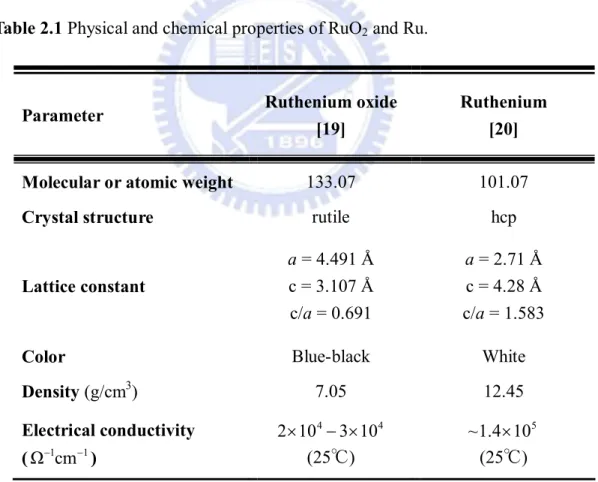
2.1 Physical and chemical properties of RuO
2and Ru
Table 2.1 Physical and chemical properties of RuO2 and Ru.
Parameter Ruthenium oxide
[19]
Ruthenium [20]
Molecular or atomic weight 133.07 101.07
Crystal structure rutile hcp
Lattice constant a = 4.491 Å c = 3.107 Å c/a = 0.691 a = 2.71 Å c = 4.28 Å c/a = 1.583
Color Blue-black White
Density (g/cm3) 7.05 12.45 Electrical conductivity (Ω cm1 1 ) 4 4 2 10 3 10 (25℃) ~1.4 10 5 (25℃)
2.2 Applications of RuO
2films
The RuO2 films can be used in Cu interconnection and capacitor electrodes [14].
The ruthenium oxide films are used in Cu interconnection because of its properties, such as low bulk resistivity, good thermal stability, and diffusion barrier capability. Furthermore, the RuO2 films demonstrate some additional advantages like a wide
potential window of reversible redox potentials, relatively high specific capacitance, and a very long cycle life. These attributes make them suitable capacitor electrodes [11]. Moreover, amorphous ruthenium oxide films have been widely used for supercapacitors owing to their high specific capacitance, high conductivity, and good electrochemical reversibility [8].
2.3 Fabrications of RuO
2films
2.3.1 Vacuum deposition
Physical Vapor Deposition (PVD)
Ruthenium oxide films have been deposited by reactive sputtering [21] and r.f. magnetron sputtering [2] instead of dc sputtering. It is because the dc sputtering can only be used to deposit conductor. In addition to typical drawbacks of PVD such as low pressure deposition condition and unnecessary waste of target, the exact control of composition is another challenge for the PVD to deposit RuO2 films.
Chemical Vapor Deposition (CVD)
Compared with RuO2 films by the PVD, the RuO2 films fabricated via the
chemical vapor deposition (CVD) have many advantages, including low cost, easy compositions control, excellent step coverage, and compatibility to large-scaled processing [22]. Unfortunately, the deposition temperature in the CVD is relatively high. In 1993, Yuan et al. used RuO4 as a precursor to deposit ruthenium oxide films
by CVD [23]. At the same year, Si et al. reported Ru(Cp)2 as a precursor to produce
polycrystalline RuO2 films by metal-organic chemical vapor deposition (MOCVD) on
three different substrates [22]. Until recently, needle-like structures of ruthenium dioxide films have been deposited with ozone-mediated CVD by Hashaikeh et al. [24]. Ozone was used to produce mixture of RuO4(g), air, and O3(g) in that research.
However, the coverage and roughness of the deposited films in that study need further improvement.
Atomic Layer Deposition (ALD)
The advantage of RuO2 films by the atomic layer deposition is that ultra thin
films can be deposited. In 2007, Jin-Hyock Kim et al. deposited ruthenium oxide films by a modified ALD with Ru(EtCp)2 precursor [14]. In comparison to the
conventional ALD for RuO2 films, polycrystalline RuO2 were deposited by this new
2.3.2 Solution deposition
Electrodeposition
In comparison to the fabrication methods mentioned above, the electrodeposition is a relatively simple, one-step, and cost-effective approach. Moreover, the electrodeposition provides advantages in preparation of uniform thin films for ruthenium oxide on substrates with complicated shapes and nanoporous structures. In 1999, Hu et al. used electrodeposition to deposit amorphous ruthenium oxide films on titanium substrates [7]. Later in 2007, the same group improved further using anodic deposition to produce amorphous ruthenium oxide films on identical substrates [13]. Similar work was done by Il-Hwan Kim et al., where ruthenium oxide films on three different substrates were obtained by electrodeposition [12]. However, roughness and denseness of the deposited films in their study were not optimized yet.
2.3.3 Other methods
In addition to vacuum deposition and solution deposition, some other methods have been reported in RuO2 films fabrication, such as organic precursor method [8],
thermal decomposition [25], and electrostatic spray deposition [11]. In 2001, Fang et
al. developed a novel organic precursor method to deposit amorphous ruthenium
oxide films under 200℃, however, the deposits become crystalline once temperature was raised above 200℃ [8]. Besides, roughness of the deposited films needs to be improved. Furthermore, Rochefort et al. used the thermal decomposition to produce RuO2 film on a Ti substrate with 150 nm thickness for 2 hr at 400℃ in 2003 [25].
Later in 2004, Il-Hwan Kim et al. took advantage of electrostatic spray deposition to produce crystalline ruthenium oxide films on different substrates [11]. However, from the cross-sectional image of the deposited films, the deposits does not seem to be sufficiently dense.
2.4 Applications of Ru films
Ruthenium films can be used as the bottom electrode and common plate materials in dynamic random access memories (DRAMs) capacitors because of their low resistivity, excellent chemical stability, and reasonable dry etching property [26]. In addition, the ruthenium has low solubility with copper. Therefore, ruthenium films are of potential to be a diffusion barrier in Cu-metallization [27].
2.5 Fabrications of Ru films
2.5.1 Vacuum deposition
Physical Vapor Deposition (PVD)
Ruthenium is a conductive metal, so most reports related to the ruthenium films deposited by PVD used a sputtering approach [3, 6, 28, 29]. In 2003, Josell et al. used the PVD to fabricate Ru films on titanium adhesion layer trenches [3]. However, the deposited films were discontinuous, and the step coverage and films continuity required optimization. On the other hand, a 5 nm amorphous ruthenium film was deposited on a silicon planar substrate by Arunagiri et al. with sputtering in 2005 [28].
Later in 2007, Jia et al. reported ruthenium films fabricated by dc sputtering [29]. Nevertheless, the deposits were oxidized to form ruthenium dioxide at elevated temperature under oxygen atmosphere. Recently, Onogawa et al. [6] have reported amorphous ruthenium/polycrystalline ruthenium on silicon oxide with sputtering.
Chemical Vapor Deposition (CVD)
Compared with ruthenium deposited by the PVD, using the CVD to deposit ruthenium film has several advantages such as ultra thin, highly conformal, and continuous ruthenium films [4]. In ruthenium films from CVD technique, the MOCVD was used with different ruthenium precursors to produce desirable deposits. In addition, the most common substrate used in this method was silicon oxide substrate. In 2004, Cho et al. used Ru(EtCp)2 as a precursor to deposit polycrystalline
Ru films on silicon oxide [4]. Besides, in 2005, Kang et al. used RuCp(i-PrCp) precursor with CVD to deposit ruthenium films on five different substrates [5]. Moreover, Kawano et al. used Ru(DMPD)(EtCp) as a precursor to produce polycrystalline ruthenium films on SiO2 substrates in both planar and trenched forms
[26]. Recently in 2007, Shin et al. used cis-RuH2(PMe3)4 to produce amorphous Ru-P
alloy films on SiO2 [30].
Although the CVD has some advantages to deposit ruthenium films, undesirable long incubation time and substrates specific dependency are two primary challenges in the CVD to produce ruthenium films [31].
Atomic Layer Deposition (ALD)
ruthenium films such as better step coverage and thickness control [27]. In 2003, Aaltonen et al. grew polycrystalline ruthenium films on borosilicate glass substrates
with RuCp2 precursor [32]. Another precursor,
2,4-(dimethylpentadienyl)(ethylcoclopentadienyl)Ru, which is also called DER, was used by Seong Keon Kim et al. with the ALD on four different substrates in 2007 [27]. However, the ALD process exhibited poor nucleation at the initial stage of the film growth. Therefore, recently Heo et al. took advantage of the UV-O3 surface treatment
to overcome this problem using identical precursor [31].
2.5.2 Solution deposition
Electrodeposition
Some research results have been reported for ruthenium films by the electrodeposition method. In 1997, Chen et al. used RuCl3 as a precursor to deposit
three monolayer ruthenium by electrodeposition [33]. Recently in 2006, Young-Soon Kim et al. took advantage of a N-bridged complex of ruthenium(IV) nitrosyl chloride formed in the plating solution to deposit ruthenium films on Ti and TiNx patterned substrates [34]. From XRD results in their study, diffraction peaks of ruthenium with broad widths suggested the deposited films were poor crystallinity. Later in the same year, this group also reported a 30 nm ruthenium thin film with grain size less than 10 nm was deposited on a titanium substrate with root mean square roughness of 8.3 nm [35]. Unfortunately, roughness for the deposited ruthenium film needed further improvement. In 2008, Thambidurai et al. used electrochemical method to deposit ruthenium films with surface limited redox replacement on Au substrates. Pb atomic layers were used in the surface limited redox replacement to control the thickness of
ruthenium nanofilms [36].
Electroless plating (ELD)
The components for the electroless Ru plating bath have been described in several studies. Table 2.2 provides the component of electroless Ru plating bath A, which was the earliest literature report for electroless Ru deposition [15]. It described four different recipes for the ruthenium plating baths. Take solution A–1 for example, the Ruthenium electroless deposition was performed in basic condition under 40℃ on copper sheet. In addition, other examples for the plating solutions were listed in Table 2.2 as well. Table 2.3 presents recent research in 2008 by Lasczek et al. for components in their ruthenium electroless plating bath [18], which we defined as the plating bath B. The components for plating bath B were similar to that of plating bath A–1 but differed in substrates. Though functions for individual component were explained carefully, relevant deposition mechanism and qualitative measurements were lacking in their study.
Another recipe for the ruthenium electroless plating was proposed by Okuno in 1990, as listed in Table 2.4 (plating bath C) [16]. The components for electroless Ru plating bath revealed negligible variation from what were listed in Table 2.2 and Table 2.3. The properties of the deposited films were examined after exposure to corrosive gases or solutions. However, qualitative characterization for the as-deposited films was still not performed.
Later in 1991, Chang et al. reported ruthenium electroless deposition with a novel plating bath recipe on silicon substrates, as shown in Table 2.5 (plating bath D) [17]. Despite reactions between the components were verified as electroless
deposition by measurement of mixed potentials, specific compounds for the addition agent was absent in Table 2.5. Moreover, we reckon that the deposition mechanism and qualitative measurement can be further investigated. On the other hand, in 2001, Ramani et al. used identical recipe except adding the addition agent in Table 2.5 described previously to deposit ruthenium particles on carbon substrates [9]. Therefore, it can be concluded that ruthenium is successfully deposited without addition of the addition agent.
Table 2.2 Components of the electroless Ru plating bath A [15]. Soln. A–1 Soln. A–2 Soln. A–3 Soln. A–4 RuCl3·3H2O 2.6 g 2.6 g – – K2[Ru(NO)Cl5] – – 3.8 g – Metal precursors [Ru(NO)(NH3)5]Cl3 – – – 3.2 g
Sodium natrite NaNO2 2.5 g 2.5 g – –
Ammonium hydroxide NH4OH (28 wt% NH3) 20 mL 20 mL 20 mL – Hydroxylamine hydrochliride NH2OH·HCl – 1.0 g 1.0 g 1.5 g Hydrochloric acid HCl – 1.0 g 1.0 g 1.5 g Hydrazine hydrate N2H4 40 wt% 0.5 mL – – 5 mL
pH 12 buffer 0.1 M NaOH plus
0.1 M Na2CO4 – – – 30 mL pH 11.8 – – 12 Temperature 40℃ – – 40 – 50 ℃ Substrate Cu ABS plastic – –
Soln. A–1 Dissolve RuCl3·3H2O in 50 mL H2O. Add a few drops of HCl and NaNO2
in small increments and boil. Add NH4OH and heat to boil. Dilute to 500
mL after cooling.
Soln. A–2 As above, except that NH4OH and hydroxylamine are added at the same
time instead of NH4OH alone.
Soln. A–3 Add hydroxylamine after boiling mixture of Ru-salt and NH4OH. Then
dilute to 500 mL.
Soln. A–4 Add Ru-salt in the buffer and heat for dissolution. Add hydroxylamine and dilute to 500 mL.
Table 2.3 Components of the electroless Ru plating bath B [18].
Ruthenium chloride RuCl3·xH2O 0.208 g/80 mL
Sodium natrite NaNO2 0.2 g/80 mL
Ammonium hydroxide NH4OH, (28 wt% NH3) 30 mL/80 mL
Sodium hydroxide NaOH 1 g/80 mL
Hydrochloric acid HCl 0.04 mL/80 mL
Hydrazine hydrate N2H4 0.75 mL/80 mL
pH 12.8
Temperature 55℃
Substrate Pd-InGaAs
Table 2.4 Components of the electroless Ru plating bath C [16].
Ruthenium salt 2.0 g/L
Ammonium hydroxide NH4OH, (28 wt% NH3) 37.5–150 mL/L
Sodium hydroxide NaOH 5–60 g/L
Hydrazine hydrate N2H4 1–6.5 g/L
pH 12.6–13.6
Temperature 55–65℃
Table 2.5 Components of the electroless Ru plating bath D [9, 17].
Reference [17] [9]
RuCl3·xH2O (40.88 wt%) 0.014 M 0.014 M
C6H14N2O7 0.014 M 0.014 M
H4NOCOCOONH4·H2O 0.07 M 0.07 M
NaOH Small amount Small amount
NaH2PO2·H2O 0.27 M 0.27 M
Addition agent Small amount –
pH 9.5 9.5
Temperature 85℃ 90℃
Chapter 3 Experimental
3.1 Experimental design
3.2 Materials
Table 3.1 Materials used in this research.
Materials
Purity
K2RuCl5·xH2O (Alfa Aesar) Ru: 25.4 wt%
NaNO2 (SHOWA) 97 wt%
NaClO (SHOWA) active Cl: 5–6 wt%
NaOH (Mallinckrodt) 99 wt% PdCl2 (Aldrish) >99 wt% HCl (SHOWA) 35–37 wt% H2 99.999 wt% Ar >99 wt% Cu substrate
3.3 Plating bath preparation
Cu specimen was used as the substrate during Ru electroless plating process. The
structures and thickness of Cu substrate is shown in Figure 3.2. First, the Cu substrate
was rinsed with acetone and water to remove impurities. Before immersing into the
plating bath, the specimen was dipped into PdCl2 aqueous solution for 10 sec at 40℃
for activation process. The components of PdCl2 aqueous solution included 0.1 wt%
plating bath was 30 mL aqueous solution which including K2RuCl5·xH2O, NaNO2,
NaOH, and NaClO. The formulation was listed in Table 3.1.
Figure 3.2 Structures of the substrate for electroless plating.
Table 3.2 Bath components and operating condition for the electroless plating.
Materials Amount Corresponding
Concentrations
Metal precursor K2RuCl5·xH2O 0.0186 g / 30 mL 1.73 10 3M
Reducing agent NaNO2
0.7038 g / 30 mL 0.0704 g / 30 mL 0.0352 g / 30 mL 0.34 M 0.034 M 0.017 M Stabilizer NaOH 0.04 g / 30 mL 0.033M
Oxidizing agent NaClO 2 mL / 30 mL
pH 11–12
The Ru plating solution was prepared by following procedure. Figure 3.3 illustrates the adding process. To begin with, NaNO2 (aq), NaOH(aq), and NaClO(aq)
were mixed together into one solution. Then the mixture was added into the Ru precursor solution at room temperature. After mixing 3 min, the plating bath turned yellow. And it gently turned orange after another 4 min. Once the plating bath turned orange, the plating bath was ready for deposition. At this moment, the pH value of the plating bath was in range from 11 to 12. And then the activated Cu substrate was dipped into the plating bath for ruthenium electroless plating with a variety of plating time at 40℃ under water bath environment. The deposition temperature was 40℃ instead of room temperature because the deposition rate at room temperature was slower than that at 40℃. After finished the plating process, the sample was moved to room temperature for 40 min in air cooling to prevent film failure by thermal stress.
3.4 Instruments and characterization
UV-Vis spectrometer
UV-Visible spectrometer (UV-Vis: Agilent 8453) was used to measure the absorption spectra of the deposition solution.
EDX
Specimens were examined by Energy Dispersive Spectrometer (EDX: JSM6500F) to check if the Ru was successfully deposited.
SEM
The morphology and thickness of the deposited thin films were obtained by a field emission scanning electron microscope (FESEM: JSM6500F or JSM6700). Ag conductive layer was coated by evaporation on the deposited films to prevent charging during measurements.
AFM
The grain size and roughness of the deposited films were measured by an atomic force microscope (AFM: Vecco Dimension 5000 Scanning Probe Microscopy).
XPS
The oxidation states of ruthenium and oxygen on the deposited films were identified by X-ray Photoelectron Spectrometer (XPS: Thermo Microlab 350).
XRD
X-ray diffractometer (HRXRD: BedeD1) was used to determine relavent phase and crystallinity of the deposited films.
Raman
Raman spectrometer was used to characterize the deposited films (Raman spectrometer LabRAM HR800).
4pp
The resistivity of the deposited films was measured by a four-point probe (CMT-SR2000N).
Chapter 4 Results and Discussion I:
Development of Ru electroless plating solution
4.1 Development of plating bath components
K2RuCl5·xH2O, and RuCl3·xH2O were the most common chloride-containing
compounds among ruthenium precursors. Between them, RuCl3·xH2O was widely
used in ruthenium related reactions. However, in most cases using the RuCl3·xH2O, a
small amount of hydrochloride acid (HCl) was added to promote RuCl3·xH2O
dissolution in water. Therefore, in our study, the K2RuCl5·xH2O was used instead to
formulate the plating bath because of its direct dissolution in water.
Figure 4.1 depicts four different mixing steps and corresponding color change for the plating baths. In Figure 4.1, all the solutions turned orange once preparation steps were complete. In comparison to Figure 3.3, these results suggested that during the plating solution preparations, the adding sequence of NaNO2(aq), NaOH(aq), and
NaClO(aq) bears negligible effect. However, the adding steps described in Figure 4.1
were much more complicated than that in Figure 3.3. Therefore, the adding steps in Figure 3.3 were selected in this study because of their relative simplicity.
Figure 4.1 Four different adding steps for the plating bath.
It is known that a pale yellow RuO4(aq) can be formed by reaction between
ruthenium precursor and sodium hypochlorite (NaClO) [37, 38]. However, because of relatively instability in sodium hypochlorite, a small amount of sodium hydroxide (NaOH) was added in sodium hypochlorite solution to prevent the dissociation of sodium hypochlorite [20]. The molar ratio for sodium hydroxide and sodium hypochlorite was fixed at 0.28 in this research because of results from previous investigation in our group [39]. Previously, the sodium nitrite (NaNO2) was used as a
complex agent [15]. However, earlier work also used hydrazine hydrate (N2H4) as a
nitrite, NaNO2(aq) was found to possess promising ability to serve as a reducing agent
in addition to a complexing agent.
To figure out the role of sodium nitrite in the plating bath, three different concentrations of NaNO2 were selected to develop plating solutions in 0.6, 0.06, and
0.03 M, respectively.The corresponding molar ratio for NaClO and NaNO2 was 0.35,
3.5, and 7, respectively.
4.2 Deposition mechanism
The deposition mechanism was proposed by the following equations, which can be further divided into two stages;
The first stage: 2
( ) 5 ( ) ( ) 4( ) ( ) 2 ( )
6OHaq 2RuCl aq 5ClOaq 2RuO aq 15Claq 3H Ol (1)
The second stage:
2 2 ( ) 4( ) 2 ( ) 4 ( ) 3 ( ) 2 ( ) 2 4 ( ) 2 ( ) 4 ( ) 2( ) ( ) 2 ( ) 4 ( ) 2 2 + (2) 3 2 2 4 (3) 2 3 aq aq aq aq aq l H O aq l OH aq aq aq l aq OH RuO NO RuO NO H O
RuO H O RuO RuO OH
H O RuO NO ( ) ( ) 2( ) 3 ( ) 2 ( ) 4 ( ) 2 ( ) ( ) ( ) 3 ( ) 2 3 (4) 2 7 2 7 (5) aq aq s aq l aq aq aq s aq OH RuO NO H O RuO NO OH Ru NO
At the first stage, during the initial 3 min right after mixing, the solution turned yellow because of the formation of dissoluble RuO4, as shown in equation (1).
However, at the second stage during the following 4 min, the solution turned orange slowly. The change of solution color resulted from the reaction between RuO4
and NaNO2, as shown in equation (2). Although the NaNO2 was commonly used as an
oxidizing agent in industry, the RuO4 has been reported as a strong and poorly-
selective oxidant [40]. Compared with the standard reduction potentials of RuO4 and
that of NaNO2, the reaction between RuO4 and NaNO2 was spontaneous in
thermodynamic, in which the RuO4 was an oxidizing agent and NaNO2 behaved as a
reducing agent. In addition, the orange RuO42– ion was one of the products in equation
(2), and its existence has been confirmed by a UV-Visible spectrum. The spectra of RuO42– ions will be further discussed in next section (section 4.3).
In addition, the RuO42– ion would underwent a disproporationation reaction to
produce RuO2 deposits and RuO4– ions, as shown in equation (3) [38]. Furthermore,
following the disproporationation in equation (3), the excess NaNO2 continued to
react with the RuO4– ions to produce RuO2 and Ru deposits, as shown in equation (4)
and equation (5), respectively.
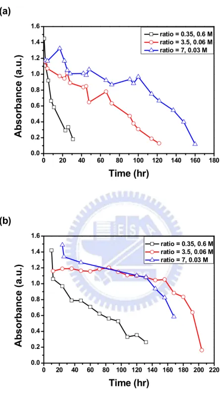
4.3 Stability of plating solution
To figure out the stability of the plating solution, a UV-Visible spectrometer was used to record the characteristic absorption peaks and the changes of absorption spectra as time progressed. Figure 4.2 displays the UV-Vis absorption spectra under the plating temperature (40 ℃ ) and room temperature with three different
concentrations of NaNO2. Take Figure 4.2 (b) for example, two absorption peaks in
the spectra were clearly observed, one was located between 350 and 375 nm (peak A), and the other was ranged from 460 to 470 nm (peak B). In addition, the absorbance of these two primary absorption peaks in Figure 4.2 (b) was decreased with longer time. Moreover, the absorbance of peak A decayed more rapidly than that of peak B as time progressed.
The curve and the position of absorption peaks from the spectra were consistent with that of RuO42– [38]. The position of peak B was consistent with the color of
plating bath, which was orange. Furthermore, the absorbance ratios of peak A and peak B were different with different concentrations of sodium nitrite. This result was attributed to the unreacted NaNO2. It was because the sodium nitrite aqueous solution
revealed an absorption peak at 350 nm which was near peak A in UV-Visible spectrum [41].
Table 4.1 summarizes the distribution of the two maximum absorption wavelengths in Figure 4.2 for the entire plating bath lifetime. The narrow distribution of the maximum absorption wavelength in the entire plating solution lifespan suggested that the species were stable rather than transforming into other species in the solution. Moreover, the lifetime of stability in Figure 4.2 (b) at 40℃ was relatively shorter compared to that in Figure 4.2 (e) at room temperature.
Figure 4.3 demonstrates the absorbance at 468 nm in UV-Visible spectra with various time under 40℃ and room temperature. With the same concentration of sodium nitrite, the absorbance in Figure 4.3 (a) decreased more rapidly than that in Figure 4.3 (b). This result indicated that the plating rate at 40℃ was faster in comparison to that at room temperature.
Figure 4.2 UV-Vis spectra of plating baths in three different ratios at various
time under 40℃ and room temperature; (a)–(c) are at 40℃, and (d)–(f) are at room temperature; (a) 0.6, (b) 0.06, (c) 0.03, (d) 0.6, (e) 0.06, and (f) 0.03 M NaNO2(aq).
200 300 400 500 600 700 800 0 1 2 3 4 A b s o rb an ce (a. u .) Wavelength (nm) 0.5 hr 2 11 23 36 (a) 200 300 400 500 600 700 800 0.0 0.2 0.4 0.6 0.8 1.0 1.2 1.4 (c) A b s o rb a n c e ( a .u .) Wavelength (nm) 2 hr 45 114 137 160 200 300 400 500 600 700 800 0.0 0.2 0.4 0.6 0.8 1.0 1.2 1.4 (b) A b s o rb a n c e ( a .u .) Wavelength (nm) 2 hr 25 66 95 122 200 300 400 500 600 700 800 0.0 0.2 0.4 0.6 0.8 1.0 1.2 1.4 1.6 (f) A b s o rb a n c e ( a .u .) Wavelength (nm) 24 hr 120 156 168 180 200 300 400 500 600 700 800 0 1 2 3 4 (d) A b s o rb a n c e ( a .u .) Wavelength (nm) 10 min 12 hr 48 96 132 200 300 400 500 600 700 800 0.0 0.2 0.4 0.6 0.8 1.0 1.2 1.4 (e) A b s o rb a n c e ( a .u .) Wavelength (nm) 10 min 48 hr 144 192 204 209
0 20 40 60 80 100 120 140 160 180 0.0 0.2 0.4 0.6 0.8 1.0 1.2 1.4 1.6 A b s o rb a n c e ( a .u .) Time (hr) ratio = 0.35, 0.6 M ratio = 3.5, 0.06 M ratio = 7, 0.03 M (a) 0 20 40 60 80 100 120 140 160 180 200 220 0.0 0.2 0.4 0.6 0.8 1.0 1.2 1.4 1.6 (b) A b s o rb a n c e ( a .u .) Time (hr) ratio = 0.35, 0.6 M ratio = 3.5, 0.06 M ratio = 7, 0.03 M
Figure 4.3 Evolution of the absorbance from the maximum absorption
wavelength of UV-Vis spectra in various time under different temperatures; (a) at 40 ℃, and (b) at room temperature.
Table 4.1 The distribution of the maximum absorption wavelength between 300 nm
and 500 nm.
Concentrations of NaNO2(aq)
(at 40℃) 300–400 (nm) (Peak A) 400–500 (nm) (Peak B) 0.03 M 368–373 462–468 0.06 M 357–365 465–468 0.6 M 349–357 463–467
Chapter 5 Results and Discussion II:
Characterization of composite RuO
2and Ru
films
5.1 Characterization of composite RuO
2and Ru
films
5.1.1 The existence of Ru element in the deposited films
The results from energy dispersive spectrometer for the deposited films with 0.06 M NaNO2(aq) at various plating time are shown in Figure 5.1. The plating time in
Figure 5.1 were 30, 60, and 240 min, respectively. In this research, when the plating time exceeded more than 30 min, the signals from ruthenium were detected by the energy dispersive spectrometer. The atomic percentage of ruthenium in EDX result increased with the plating time. As the plating time was 30 min, the atomic percentage of Ru was 0.77%. When the plating time reached 60 and 240 min, respectively, the atomic percentages of ruthenium increased up to 1.66% and 3.95%. The results suggested a sustained growth of Ru.
Figure 5.1 EDX results from the deposited films with 0.06 M NaNO2(aq) at
various plating time; (a) 30, (b) 60, and (c) 240 min, respectively. (d)–(f) were the corresponding spectrum.
(b)
(c)
(d)
(f)
(a)
(e)
5.1.2 Morphology observation and thickness measurement of
the deposited films
Figure 5.2 presents the planar views of deposited films at various plating time with 0.6 M NaNO2(aq). The plating time were 30, 60, 120, 240, and 480 min,
respectively. For instance, in Figure 5.2 (a), when the plating time was 30 min, the planar view was uniform with small particles. The existence for these small particles inferred that the deposited films grew continually. This finding was consistent with the results from EDX as described previously. The deposited films remained uniform as the plating time was increased up to 120 min. However, when the plating time was further up to 240 min, films with cracks were easily observed in the SEM image, as shown in Figure 5.2 (d). It was worth noting that the position of cracks was near the location of particles. In addition, the deposited film cracked as the plating time reached 480 min, as shown in Figure 5.2 (e). This finding indicates the cracking on the deposited film is attributed to the internal stress rather than thermal stress because temperature gradient in all samples remains unchanged, which is from 40℃ to room temperature. The results described above were similar to the deposited films with lower concentrations of sodium nitrite, 0.06 and 0.03 M, as shown in Figure 5.3 and Figure 5.4, respectively.
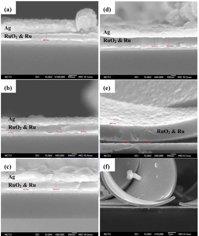
Figure 5.5 provides the cross-sectional views of the deposited films at various plating time with 0.06 M NaNO2(aq). In order to observe the deposited films with
cross-sectional views, a silver conducting layer was deposited by evaporation on the deposited films in Figure 5.5 (a) to (d) to prevent the edge charging of SEM. Figure
5.5 (e) was not deposited with a conducting layer because of the crack of deposited film. In addition, Figure 5.5 (f) was the smaller scope of Figure 5.5 (e) for the same sample, in which the deposited film was bended because of a larger internal stress. In Figure 5.5 (a), for example, the cross-sectional view for the deposited film was smooth and the thickness of that was uniform. Besides, the thickness of the deposited films increased with the plating time. It is important to note that the deposited films remain relatively smooth even though the thickness of the deposited films increased with the plating time.
Figure 5.2 Planar views for the deposited films at various plating time with 0.6
M NaNO2(aq); (a) 30, (b) 60, (c) 120, (d) 240, and (e) 480 min, respectively.
(a)
(b)
(c)
(d)
Figure 5.3 Planar views for the deposited films at various plating time with 0.06
M NaNO2(aq); (a) 30, (b) 60, (c) 120, (d) 240, and (e) 480 min, respectively.
(a)
(b)
(c)
(d)
Figure 5.4 Planar views for the deposited films at various plating time with 0.03
M NaNO2(aq); (a) 30, (b) 60, (c) 120, (d) 240, and (e) 480 min, respectively.
(a)
(b)
(c)
(d)
Figure 5.5 Cross-sectional views for the deposited films at various plating time
with 0.06 M NaNO2(aq); (a) 30, (b) 60, (c) 120, (d) 240, and (e) 480 min, respectively;
and (f) the smaller scope of (e).
(a)
(b)
(c)
(d)
(e)
Ag RuO2 & Ru Ag RuO2 & Ru Ag RuO2 & Ru Ag RuO2 & Ru RuO2 & Ru(f)
5.1.3 Thickness at different plating time
The thicknesses of the deposited films versus various plating time with different concentrations of sodium nitrite are shown in Figure 5.6. The thickness of the deposited film ranged from 35–300 nm at the selected plating time. In addition, the slope in Figure 5.6 revealed the deposition rate at various periods of time with different concentrations of sodium nitrite. As the plating time was increased, the deposition rate gradually decreased. This result was attributed to the reduction of diffusion rate of ruthenium-containing ions in the plating solutions. In other words, the concentration of ruthenium-containing ions decreases with the increasing time, which leads to the reduction of diffusion rate. As a result, the deposition rate is decreased as well. 0 100 200 300 400 500 0 50 100 150 200 250 300 T h ic k n e s s (n m ) Time (min) ratio = 0.35, 0.6 M ratio = 3.5, 0.06 M ratio = 7, 0.03 M
Figure 5.6 Thicknesses for the deposited films versus various plating time with
5.1.4 Roughness measurement for the deposited films
The roughness for the deposited films at three different concentrations of NaNO2(aq) with various plating time are showed in Figure 5.7. The values of root
mean square of the roughness (Rq) in the deposited films under selective plating time
with various concentrations of NaNO2(aq) were listed in Table 5.1. From Table 5.1, as
plating time was increased, the Rq values of the deposited films were increased as
well. In addition, when the deposition time was 120 min, the uniformity of the deposited films was decreased with increase of the concentrations of NaNO2(aq), as
shown in Table 5.1. Moreover, the uniformity at 120 min plating time with various concentrations of NaNO2(aq) were 2.05%, 4.59%, and 6.70%, respectively. Therefore,
combining the results of plating solution lifetime and that of roughness, it is concluded that the recipe for the plating solution with 0.06 M NaNO2(aq) is more
applicable than other two concentrations.
Table 5.1 Rq of the deposited films under selective plating time in different
concentrations of NaNO2(aq).
Plating time
Concentration of NaNO2(aq)
10 min 120 min Uniformity at
120 min
0.6 M 2.358 nm 3.427 nm 2.05%
0.06 M 3.121 nm 4.593 nm 4.59%
Figure 5.7 Roughness of the deposited films at three different concentrations of
NaNO2(aq) in various plating time; (a)–(c) are at 10 min, and (d)–(f) are at 120 min; (a)
0.6, (b) 0.06, (c) 0.03, (d) 0.6, (e) 0.06, and (f) 0.03 M NaNO2(aq).
(a)
(b)
(c)
(d)
(e)
(f)
5.1.5 Characterization of the oxidation states for the deposited
films
The oxidation states for the deposited films were determined by the electron spectroscopy for chemical analysis (ESCA), which was measured by a X-ray photoelectron spectrometer. We selected the ruthenium and oxygen to measure, using their spectral lines of 3p3/2 and 1s, respectively. Figure 5.8 provides the XPS spectra of Ru 3p3/2 line for the deposited films with 0.06 M NaNO2(aq) with various plating
time, 30, 120, and 480 min, respectively. Similarly, Figure 5.9 displays the corresponding XPS spectra for the O 1s line.
Figure 5.8 exhibits the XPS spectra for the Ru 3p3/2 line from the deposited films at various plating time with 0.06 M NaNO2(aq). From XPS spectra in Figure5.8,
a signal of Ru 3p3/2 line was observed, which suggested the presence of ruthenium element in the deposits. This observation was consistent with the results from EDX in Figure 5.1.
In Figure 5.8, the positions of binding energy with maximum intensity in Ru 3p3/2 line were nearly the same. They were located at 464, 464, and 464.2 eV, respectively. This result indicates that the oxidation states for ruthenium from the deposits during the entire plating procedure are identical regardless of the length for the deposition process. The corresponding binding energies with maximum intensity in Figure 5.9 for the O 1s line were at 531.3, 531.1, and 531.2 eV, respectively. This finding suggested that the composition for oxygen in the deposits remained unchanged at different deposition time with the same sodium nitrite concentration.
However, these findings are limited to surface of the deposited films because of shallow depth resolution of XPS. The change of the deposits below depth resolution of XPS during the plating process requires further investigation, such as depth profiling by Auger electron spectrometer (AES).
Furthermore, the entire spectrum for the O 1s line, shown in Figure 5.9 as a shoulder at higher binding energy ranging from 540 to 535 eV, was observed. This result confirms the presence of metal oxides in the deposited films because a shoulder in the O line spectrum is a character for metal oxide. Therefore, this finding indicates that the ruthenium oxides are likely to exist in the deposited films.
To determine the exact compositions for the deposited films, a curving fitting was performed to decide relatively percentage of Ru materials. Figure 5.10 shows the XPS spectra of Ru 3p3/2 line for both experimental and curve fitting lines from the deposited film with 0.6 M NaNO2 for 30 min plating time. From the results of curving
fitting, we determined Ru metal, RuO2·nH2O, and RuO3 simultaneous existed in the
deposited film. The positions for the binding energy for these three materials were assigned to 462.2, 463.8, and 466.9 eV, respectively. Relative percentages of ruthenium containing materials after the curve fitting in Figure 5.10 were described as follows. The amounts of Ru, RuO2·nH2O, and RuO3 in the deposited film after curve
fitting were 11.72%, 68.97%, and 19.31%, respectively, as listed in Table 5.2. The existence of Ru and RuO2·nH2O confirms that the deposited film is a Ru and
RuO2·nH2O composite film. However, the existence of RuO3 in the composite film
was a pressing problem. The existence of RuO3 was attributed to two possible reasons.
One possibility for the presence of RuO3 was that the RuO3 was formed by surface
deposited film, acting as an impurity trapped by RuO2·nH2O in the composite film
[10].
In comparison to Figure 5.10, Figure 5.11 and Figure 5.12 were the XPS spectra for the Ru 3p3/2 line of experimental and curve fitting from the deposited films for the same plating time with different concentrations of NaNO2(aq), 0.06 and 0.03 M,
respectively. The results of curve fitting for the percentage of ruthenium compounds were listed in Table 5.2.
Table 5.2 provides the relative amounts of Ru in different forms in XPS spectra from Figure 5.10 to Figure 5.12. In Table 5.2, as the concentration of NaNO2(aq) was
increased, the percentage of RuO3 was decreased. The result was attributed to the rate
of deposition. The deposition rate was increased with increasing concentration of NaNO2(aq). As the concentration of NaNO2(aq) was increased, the concentration
gradient was increased in the diffusion layer within the plating solution. Therefore, the ions refilling rate is enhanced with the concentration of NaNO2(aq). In other words,
a higher concentration of NaNO2(aq) leads to much less amount of RuO3 because the
475 470 465 460 2.4x10⁴ 2.7x10⁴ 3.0x10⁴ 3.3x10⁴ 3.6x10⁴ 475 470 465 460 1.8x10⁴ 2.1x10⁴ 2.4x10⁴ 475 470 465 460 2.4x10⁴ 2.7x10⁴ 3.0x10⁴ 3.3x10⁴ 464.2
Binding Energy (eV)
(c) 480 min 464 In te n s it y ( c o u n ts /s ) (b) 120 min (a) 30 min 464
Figure 5.8 XPS spectra for the Ru 3p3/2 line from the deposited films with 0.06
M NaNO2(aq) at various plating time; (a) 30, (b) 120, and (c) 480 min, respectively.
540 535 530 525 3.2x10⁴ 4.0x10⁴ 4.8x10⁴ 5.6x10⁴ 540 535 530 525 2.4x10⁴ 3.2x10⁴ 4.0x10⁴ 4.8x10⁴ 540 535 530 525 3.2x10⁴ 4.0x10⁴ 4.8x10⁴ 5.6x10⁴ 531.2 531.1 531.3
Binding Energy (eV)
(c) 480 min In te n s it y ( c o u n ts /s ) (b) 120 min (a) 30 min
Figure 5.9 XPS spectra for the O 1s line from the deposited films with 0.06 M
474 472 470 468 466 464 462 460 458 456 0 4.5x10⁴ 5.0x10⁴ 5.5x10⁴ 6.0x10⁴ 6.5x10⁴ In te n s it y ( c o u n t/ s )
Binding Energy (eV)
(a) Background (b) Experimental (c) Ru (d) RuO2 nH2O (e) RuO3 (f) Curve fitting
Figure 5.10 XPS spectra for the Ru 3p3/2 line including both experimental and
curve fitting of the deposited film with 0.6 M NaNO2(aq) for 30 min plating time.
474 472 470 468 466 464 462 460 458 456 0.0 2.4x10⁴ 2.6x10⁴ 2.8x10⁴ 3.0x10⁴ 3.2x10⁴ In te n s it y ( c o u n t/ s )
Binding Energy (eV)
(a) Background (b) Experimental (c) Ru (d) RuO2 nH2O (e) RuO3 (f) Curve fitting
Figure 5.11 XPS spectra for the Ru 3p3/2 line including both experimental and
474 472 470 468 466 464 462 460 458 456 0.0 2.2x10⁴ 2.4x10⁴ 2.6x10⁴ 2.8x10⁴ 3.0x10⁴ 3.2x10⁴ 3.4x10⁴ In te n s it y ( c o u n t/ s )
Binding Energy (eV)
(a) Background (b) Experimental (c) Ru (d) RuO2 nH2O (e) RuO3 (f) Curve fitting
Figure 5.12 XPS spectra for the Ru 3p3/2 line including both experimental and
curve fitting of the deposited film with 0.03 M NaNO2(aq) for 30 min plating time.
Table 5.2 Relative amounts of Ru in different forms from XPS spectra from Figure
5.10 to Figure 5.12.
Materials RuO3 RuO2·nH2O Ru
(466.9 eV) (463.8 eV) (462.2 eV)
0.6 M 19.31% 68.97% 11.72%
0.06 M 21.29% 64.52% 14.19%
5.1.6 Phase and crystallinity characterization for the deposited
films
Figure 5.13 displays the XRD pattern for the as-deposited films with various concentrations NaNO2(aq) for 480 min plating time versus Ru (JCPDS No: 060663)
and RuO2 (JCPDS No: 401290). Because the compositions during the deposition
process were identical, the composite films with 480 min plating time for different NaNO2(aq) concentrations were selected to undergo XRD analysis. From Figure 5.13
(a) to Figure 5.13 (c), we did not observe typical crystalline diffraction peaks. Instead, a broad diffraction peak from 30 to 40 was appearing. In addition, in comparison to the standard XRD patterns, we did not observe ruthenium or ruthenium oxide peaks. These results indicated that the as-deposited composite films with different amounts of NaNO2(aq) were amorphous in nature.
20 30 40 50 60 70 0 50 100 150 20 30 40 50 60 70 0 100 200 20 30 40 50 60 70 0 100 200 20 30 40 50 60 70 0 100 200 (1 0 0 ) (0 0 2 ) (101) (211) (101) (110) Ru RuO2 In te n s it y ( a .u .) 2
(a) 0.03 M In te n s it y ( c p s ) (b) 0.06 M (c) 0.6 MFigure 5.13 XRD patterns for the as-deposited films with various concentrations
of NaNO2(aq) for 480 min plating time versus the standard pattern; (a) 0.03 (b) 0.06,
and (c) 0.6 M, respectively.
5.1.7 Raman spectroscopy characterization for the deposited
films
Raman spectra for the composite films with 0.6 M NaNO2(aq) at various plating
time is shown in Figure 5.14. Also displayed is the signal from the Cu stbstrate. As the previous research had suggested, stretching modes of RuO2 in Raman spectra were
located at 515 and 626 cm–1, respectively [33, 42]. From Figure 5.14 (a) and Figure 5.14 (b), a broad peak around 500 cm–1 was observed for the composite film with 30
![Table 2.2 Components of the electroless Ru plating bath A [15]. Soln. A–1 Soln. A–2 Soln](https://thumb-ap.123doks.com/thumbv2/9libinfo/8598587.190029/25.892.154.792.165.719/table-components-electroless-plating-bath-soln-soln-soln.webp)