* Corresponding author. Fax: #1-480-965-7954. E-mail address: [email protected] (K.T. Tsen)
Physica B 272 (1999) 416}418
Ballistic electron transport in InP observed by subpicosecond
time-resolved Raman spectroscopy
K.T. Tsen
!,*, D.K. Ferry", Jye-Shyang Wang#, Chao-Hsiung Huang#,
Hao-Hsiung Lin
#
!Department of Physics and Astronomy, Arizona State University, Tempe, AZ 85287, USA "Department of Electrical Engineering, Arizona State University, Tempe, AZ 85287, USA #Department of Electrical Engineering, National Taiwan University, Taipei, Taiwan, ROC
Abstract
Electron ballistic transport in an InP-based p}i}n nanostructure under the application of an electric "eld has been studied by time-resolved Raman spectroscopy at ¹"300 K. The time evolution of electron distribution, electron drift velocity has been directly measured with subpicosecond time resolution. Our experimental results show that, for a photoexcited electron}hole pair density of n+5]1016 cm~3, electrons travel quasi-ballistically} electron drift velocity increases linearly with time, during the "rst 150 fs. After 150 fs it increases sublinearly until reaching the peak value at about 300 fs. The electron drift velocity then decreases to its steady-state value. ( 1999 Elsevier Science B.V. All rights reserved.
Keywords: Ballistic transport; Raman spectroscopy; Electron distributions
As the size of semiconductor devices becomes smaller than 1lm, the time scale important for device operation becomes quite short. In these short time regimes, which is typically in the order of subpicosecond, the transport properties of elec-trons are known to be very di!erent from those observed under steady-state conditions. One of the interesting phenomena arising is the so-called `electron velocity overshoota, where electron drift velocity overshoots its steady-state value. This po-tential for greatly enhancing the operating speed of a semiconductor device has attracted a lot of
atten-tion [1,2]. With the advent of ultrafast pulsed laser sources, it is now possible to directly observe such a transient electron transport phenomenon in semi-conductors. Theoretically, the transient electron transport properties have been extensively studied by Ruch [3], and Maloney and Frey [4] in Si and GaAs. Experimentally, several research groups [5}12] have developed di!erent experimental tech-niques in an attempt to observe such a novel transi-ent transport phenomenon in Si, GaAs and GaAs quantum wells. Recently, Grann et al. [13] have studied electron velocity overshoot and LO phonon dynamics in a GaAs-based p}i}n nanos-tructure semiconductor by using subpicosecond Raman spectroscopy. Non-equilibrium electron distributions, LO phonon populations and electron
0921-4526/99/$ - see front matter ( 1999 Elsevier Science B.V. All rights reserved. PII: S 0 9 2 1 - 4 5 2 6 ( 9 9 ) 0 0 3 1 3 - 0
Fig. 1. Electron distribution for an InP nanostructure taken at ¹"300 K, n+5]1016 cm~3, an electric "eld intensity of
E"15 kV/cm and at a time delay of*t"120 fs.
drift velocities as a function of electron density and electric "eld intensity in GaAs were directly measured. In this paper, we demonstrate that time-resolved Raman spectroscopy can also be used to study ballistic electron tranport. We have observed that in InP nanostructures, for electric "eld inten-sity of E"15 kV/cm, and electron}hole pair
den-sity of n+5]1016 cm~3, electrons travel
ballistically during the "rst 150 fs of their transient. The InP p}i}n nanostructure sample investi-gated in this work was grown by molecular beam epitaxy on a (0 0 1)-oriented InP substrate. The p-type layer was made up of a 100 As -thick Be-doped (+1017 cm~3) InP layer. The i-type region was a 1lm-thick intrinsic InP. This was the active volume probed by our experiment. The n-type layer consisted of a 1000 As -thick Si-doped (+1017 cm~3) InP layer. The p-type and n-type layers served as plates of a capacitor which provided a uniform electric "eld across the intrinsic InP layer. The mesa-like nanostructure p}i}n sample had a circu-lar opening of diameter +500 lm. This opening made the light scattering experiments possible.
The laser used in this experiment had a photon energy of 1.51 eV and a pulse width of +100 fs. These ultrashort pulses were generated by a cw
mode-locked Ti}sapphire laser. The probe
pulses consist of a train of pulses having photon energy+u"1.51 eV; whereas the pump pulses are
derived from their second harmonic, i.e.,
+u"3.02 eV. The photoexcited electron}hole pair density was estimated from the power density per laser pulse, the laser spot size on the sample and the penetration depth of the laser under our experimental conditions. This experimental ar-rangement is to make sure that no electrons escape from the probe region during the transient measurements.
The single-particle scattering (SPS) experiments were carried out in the backscattering geometry with Z(X, >)ZM scattering con"gurations for the probe pulses; where X"(1 0 0), >"(0 1 0) and
Z"(0 0 1). Since the SPS cross section is inversely
proportional to the e!ective mass of the carriers [14,15], our experiment primarily probes electron transport in the C-valley, even though holes are simultaneously present. We note that, under re-verse-biased conditions, our backscattering
ge-ometry probes the electron distribution along the direction of !Eo . All of the experimental data re-ported here were performed at ¹"300 K. The scattered light was collected and analyzed by a double spectrometer and a photomultiplier tube. The e!ective average electric "eld intensity during the transient was determined by using Franz}Kel-dysh e!ect [16].
Fig. 1 shows a typical electron distribution func-tion for an InP nanostructure taken at n+5] 1016 cm~3, an electric "eld intensity of E" 15 kV/cm and at a time delay of*t"120 fs. Elec-tron distribution shifts toward !Eo direction, as expected. A sharp cut-o! in the velocity distribu-tion around 1.4]108 cm/s is observed, indicating the onset of electron intervalley scattering pro-cesses in InP. The distribution clearly cannot be "t by a shifted Fermi}Dirac function which re#ects the extremely non-equilibrium nature of electron distribution under the application of an electric "eld. The electron drift velocity for a given electron distribution function was calculated in a straight-forward way by taking a weighted average over the electron velocity distribution.
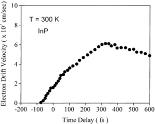
Fig. 2 shows electron drift velocity as a function of the time dealy for an InP nanostructure taken at
n+5]1016 cm~3 and at an electric "eld intensity of E"15 kV/cm. We have found that, for a
Fig. 2. Electron drift velocity as a function of the time delay for an InP nanostructure. The linearly increased velocities between 0 and 150 fs were attributed to the ballistic transport of electrons during the transient.
photoexcited electron}hole pair density of n+5] 1016 cm~3, electrons travel quasi-ballistically } electron drift velocity increases linearly with time, during the "rst 150 fs. After 150 fs it increases sublinearly until reaching the peak value of about 8]107 cm/s at about 300 fs. The electron drift velocity then decreases to its steady-state value. Apparently, for the "rst 150 fs of the transient, electrons su!er very minimal scattering. As a result the drift velocity increases linearly with the elapsed time.
In conclusion, we demonstrate that time-res-olved Raman spectroscopy can also be used to directly study ballistic electron tranport. We have observed that in InP nanostructures, for electric "eld intensity of E"15 kV/cm, and electron} hole pair density of n+5]1016 cm~3, electrons travel ballistically during the "rst 150 fs of their transient.
Acknowledgements
This work was supported by the National Sci-ence Foundation under Grant No. DMR-9301100.
References
[1] D.K. Ferry, H.L. Grubin, G.J. Iafrate, in: R.R. Alfano (Ed.), Semiconductors Probed by Ultrafast Laser Spectroscopy, Vol. 1, Academic Press, New York, 1984, p. 413. [2] E. Constant, in: L. Reggiani (Ed.), Hot Electron Transport
in Semiconductors, Springer, Berlin, 1985, p. 227. [3] J.G. Ruch, IEEE Trans. Electron. Devices ED-19 (1972)
652.
[4] T.J. Maloney, J. Frey, J. Appl. Phys. 48 (1977) 781. [5] M.S. Shur, L.H. Eastman, Solid State Electron. 24 (1981)
11.
[6] C.V. Shank, R.L. Fork, B.I. Greene, F.K. Reinhart, R.A. Logan, Appl. Phys. Lett. 38 (1981) 104.
[7] K.E. Meyer, M. Pessot, G. Mourou, R.O. Grondin, S.N. Chaoun, Appl. Phys. Lett. 53 (1988) 2254.
[8] J. Son, W. Sha, J. Kim, T.B. Norris, J.F. Whitaker, G.A. Mourou, Appl. Phys. Lett. 63 (1993) 923.
[9] E.D. Grann, S.J. Sheih, C. Chia, K.T. Tsen, O.F. Sankey, S.E. Guncer, D.K. Ferry, G. Maracas, R. Droopad, A. Salvador, A. Botcharev, H. Morkoc, Appl. Phys. Lett. 64 (1994) 1230.
[10] E.D. Grann, K.T. Tsen, O.F. Sankey, D.K. Ferry, A. Salva-dor, A. Botcharev, H. Morkoc, Appl. Phys. Lett. 67 (1995) 1760.
[11] E.D. Grann, S.J. Sheih, K.T. Tsen, O.F. Sankey, S.E. Gun-cer, D.K. Ferry, A. Salvador, A. Botcharev, H. Morkoc, Phys. Rev. B 51 (1995) 1631.
[12] E.D. Grann, K.T. Tsen, D.K. Ferry, A. Salvador, A. Botcharev, H. Morkoc, Phys. Rev. B 53 (1996) 9838. [13] E.D. Grann, K.T. Tsen, D.K. Ferry, A. Salvador, A.
Botcharev, H. Morkoc, Phys. Rev. B 56 (1997) 9539. [14] M.V. Klein, in: M. Cardona, G. Guntherodt (Eds.), Light
Scattering in Solids I, Springer, Berlin, 1983, p. 147. [15] G. Abstreiter, M. Cardona, A. Pinczuk, in: M. Cardona, G.
Guntherodt (Eds.), Light Scattering in Solids IV, Springer, Berlin, 1983, p. 5.
[16] K.T. Tsen, R.P. Joshi, A. Salvador, A. Botcharev, H. Morkoc, J. Appl. Phys. 81 (1997) 406.