memory applications. In contrast to other methods of forming DL metal NC, the IB technique is a relatively simple fabrication method and completely compatible with the current IC man-ufacturing technologies. Using the IB technique, a high-quality ultrathin interlayer between top and bottom layered NCs can be easily formed and controlled. Compared with the control sample, the IB-induced DL Ni NC memory exhibits superior performance in terms of faster program and erase (P/E) speeds, longer data retention, better endurance, negligible program disturbance, and great potential for a multilevel operation. In addition, the IB-induced DL Ni NC device also shows higher P/E efficiency as well as similar excellent reliability by comparison with other conventional DL metal NC memories due to the high-quality ultrathin interlayer.
Index Terms— Double-layer metal nanocrystal, ion bombard-ment (IB), nickel, nonvolatile memory (NVM).
I. INTRODUCTION
R
ECENTLY, floating-gate nonvolatile memory (NVM) has been actively investigated and widely applied to portable electronic productions, such as smart phone, tablet PC, and global positioning system. As the device size is continuously shrunk, however, the conventional floating-gate structure will face serious reliability challenges [1]–[6]. To smoothly promote NVM scaling down, various discrete storage layers have been proposed to replace a continuous poly-Si storage layer in the floating-gate structure, such as high-k trapping layer [7]–[9], semiconductor dots [10]–[12], and metal nanocrystals (NCs) [13]–[15]. Among various discrete storage layers, double-layer (DL) metal NC has attracted Manuscript received May 16, 2013; revised July 3, 2013; accepted August 16, 2013. Date of publication September 5, 2013; date of current version September 18, 2013. This work was supported in part by the National Science Council of Taiwan under Contract NSC-101-2221-E-035-035 and the Nano Device Laboratories. The review of this paper was arranged by Editor K. Roy.S.-H. Liu is with the Ph.D. Program of Electrical and Communica-tions Engineering, Feng Chia University, Taichung 40724, Taiwan (e-mail: [email protected]).
W.-L. Yang is with the Department of Electronic Engineering, Feng Chia University, Taichung 40724, Taiwan (e-mail: [email protected]).
Y.-H. Lin is with the Department of Electronic Engineering, National United University, Miaoli 36003, Taiwan (e-mail: [email protected]).
C.-C. Wu is with the Graduate Institute of Biomedical Materials and Tissue Engineering, the College of Oral Medicine, Taipei Medical University, Taipei 11031, Taiwan (e-mail: [email protected]).
T.-S. Chao is with the Department of Electrophysics, National Chiao Tung University, Hsinchu 30010, Taiwan (e-mail: [email protected]).
Color versions of one or more of the figures in this paper are available online at http://ieeexplore.ieee.org.
Digital Object Identifier 10.1109/TED.2013.2279156
several fabrication methods have been proposed, such as repeating dip-coating process (RDCP) [16], thermal silicida-tion reacsilicida-tion (TSR) [17], and multistep deposisilicida-tion (MSD) [18]–[21]. For the RDCP, it employs a poly (styrene-b-methyl methacrylate) diblock copolymer as an etching mask to form fillisters in the dielectric layer for self-aligned DL metal NC. The symmetry between top-layered (TL) and bottom-layered (BL) metal NCs can be easily controlled, but the NC size is not easily shrunk. Moreover, this process is very complex and incompatible with the standard CMOS process. For the TSR, it utilizes silicidation reaction between silicon and silicide metal atoms to directly embed DL metal-silicide NC in the dielectric. During formation of DL metal NC, a large thermal budget is required for silicidation reaction and diffusion between silicon and silicide metal atoms. This method limits the selection of metal NC materials. For the MSD, it uses a repeating single-layer (SL) metal NC process. So far, this method has been the most popular and direct fabrication method. The MSD has been developed to realize various DL metal NCs, but complex processes and a high manufacturing cost are unavoidable due to repeating and interlaced physical vapor deposition (PVD), chemical vapor deposition (CVD), and thermal-annealing processes.
To improve the above drawbacks, a novel ion bombardment (IB) technique is presented to fabricate a DL metal NC. Compared with other fabrication methods, the IB technique is a relatively simple process. Using the IB technique, complex and high-cost processes can be avoided. Also, the IB technique is completely compatible with the current IC manufacturing technologies. On the other hand, the IB-induced DL metal NC memory possesses a high-quality and ultrathin interlayer between TL and BL NCs. Due to the high-quality ultrathin interlayer, the IB-induced DL metal NC memory has higher program and erase (P/E) efficiency and similar excellent reliability by comparison with other DL metal NC memories fabricated by general method.
In this paper, a TaN/Al2O3/Si3N4/SiO2/Si (TANOS) NVM with embedded IB-induced DL metal NC was fully studied. We employed the Ni element as the material of DL metal NC. This is because, in contrast to other metal NC materials, the Ni material has been completely compatible with the current IC manufacturing technologies and widely used in the semiconductor industry [22]–[25]. In addition, the Ni NC also has a great storage capability due to the high work function [26]. The sizes and densities of the IB-induced DL 0018-9383 © 2013 IEEE
Fig. 1. Process flow diagrams of the SL, IB-induced DL, and conventional DL metal NCs.
Ni NC were analyzed by high-resolution transmission electron microscopy (HR-TEM). The performance and reliability of the IB-induced DL Ni NC memory, including P/E speeds, data retention, device endurance, and program disturbance properties, were also investigated in this paper.
II. DEVICEFABRICATION
The samples were prepared on <100> p-type silicon wafers. After local oxidation of silicon formation, a 3-nm thick tunneling SiO2 film was thermally grown by vertical furnace in N2O ambient, and then a 5.4-nm thick bottom Si3N4 film was deposited by low pressure CVD. Subsequently, a 5-nm thick Ni film was deposited by E-gun evaporation. Next, an Ar IB treatment for 5 s was performed on the Ni thin film by high density plasma CVD. The RF and DC were set at a power of 200 and 20 W, respectively. After the Ar IB process, partial Ni atoms of the Ni film sank into the bottom Si3N4film due to physical impact. Afterward, a 500 °C for 30-s thermal annealing was used for forming a DL Ni NC. A 3-nm thick top Si3N4and 12-nm thick blocking Al2O3were sequentially deposited by plasma enhanced CVD and metal organic CVD, respectively. A TaN control gate was then deposited by sputter. Finally, the standard n-MOSFET process was followed to complete a TANOS NVM device with embedded IB-induced DL Ni NC. In addition, a device without Ar IB treatment was also prepared as a control sample, namely, SL Ni NC memory. The channel width and length of the devices were 10 and 0.35µm, respectively. The structural analyses of Ni NCs were performed by HR-TEM, and the electrical characteristics were demonstrated by Keithley 4200 system.
III. RESULTS ANDDISCUSSION
Fig. 1 shows process flow diagrams of the SL, IB-induced DL, and conventional DL metal NCs. It is observed that a SL metal NC can be obtained by an ultrathin metal film and competent thermal-annealing process. As processed by thermal annealing, an ultrathin metal film self-assembles into a SL
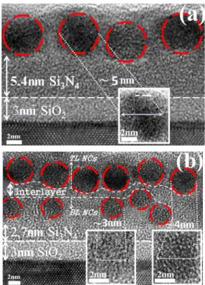
Fig. 2. Cross-sectional HR-TEM images of 5-nm thick Ni films (a) without and (b) with Ar IB treatment after 500 °C for 30-s thermal annealing. metal NC [14]. However, the conventional DL metal NC is fabricated by repeating the formation method of SL metal NC [18]–[21]. Repeating and interlaced PVD, CVD, and thermal-annealing processes would increase the manufacturing cost and decrease the processing stability. Additionally, the MSD and thermal stresses easily cause a large number of shallow deficiencies around NCs during formation of DL metal NC to result in serious charge loss problems, especially in high-temperature environment [27]–[29]. Using the IB technique, however, this complex and high-cost fabrication method of DL metal NC can be improved. While an ultrathin metal film is treated by Ar IB treatment, partial metal atoms of the metal film could sink into the bottom dielectric due to physical impact of Ar plasma. Subsequently, a DL metal NC can be formed after thermal annealing. As can be observed easily, by comparison with the conventional fabrication method, the IB technique is a relatively simple fabrication method. Also, the IB technique is completely compatible with the standard CMOS process [30]. On the other hand, it is worth noting that the interlayer between the IB-induced TL and BL NCs is from the original bottom dielectric. For the conventional DL metal NC, however, the formation of the interlayer between TL and BL NCs must rely on additional CVD deposition.
Fig. 2 shows the HR-TEM images of 5-nm thick Ni films with and without IB treatment after 500 °C for 30-s thermal annealing, respectively. From Fig. 2(a), it is shown that a 5-nm thick Ni film without IB treatment directly transforms into a SL Ni NC after 500 °C for 30-s thermal annealing. The size of the SL Ni NC is estimated to be ca. 5 nm. Meanwhile, a 5-nm thick Ni film with IB treatment transforms into a DL Ni NC after 500 °C for 30-s thermal annealing, as shown in Fig. 2(b). The sizes of the TL and BL Ni NCs are estimated
Fig. 3. (a) Program and (b) erase characteristics of the TANOS memories with embedded SL and IB-induced DL Ni NCs under different applied voltages. As to the erase measurement, the devices were initially operated at the program state, that was, Vth–initial Vth = 3 V. The fresh threshold voltages (Vth) of the TANOS memories with embedded SL and IB-induced DL Ni NCs are 0.9 and 0.74 V, respectively. The Vthis defined as the applied gate voltage when the drain current is 100 nA during operation mode.
to be ca. 4 and 3 nm in diameter, respectively. In addition, the average thickness of the interlayer between the TL and BL Ni NCs is smaller than 2 nm. As can be observed easily, a DL metal NC can be realized by the IB technique. On the other hand, because all of the Ni NCs are almost sphere, the densities of the TL and BL Ni NCs can be calculated from the 1-D TEM image. The 1-D densities of the TL and BL Ni NCs are estimated to be ca. 2.07× 10⁶and 1.62× 10⁶#/cm, respectively. Consequently, the 2-D densities of the TL and BL Ni NCs can be further obtained to be ca. 4.28× 10¹²and 2.62× 10¹²#/cm2, respectively. For the SL Ni NC, likewise, the 2-D NC density can be estimated to be ca. 2.9× 10¹² #/cm2.
Fig. 3 shows the P/E characteristics of the TANOS mem-ories with embedded SL and IB-induced DL Ni NC. The memory window is defined as a threshold voltage change (Vth shift) of a device between P/E states. The Fowler– Nordheim tunneling was employed for programming and erasing. From Fig. 3, it is shown that the P/E speeds and memory windows are increased with increasing the applied voltage for the TANOS memories with an embedded Ni NC. As can be observed in Fig. 3(a), the IB-induced DL Ni NC device exhibits a faster program speed and larger memory window than the SL Ni NC sample. Under VP = 17 V
the same erasing condition for the SL Ni NC sample. These improvements in P/E efficiency are attributed to an increase in the number of NCs, 3-D distribution of NCs, and DL metal NC-induced strong coupling with conduction path [31]. On the other hand, as compared with other DL metal NC memories fabricated by general method [16]–[21], the IB-induced DL Ni NC has superior P/E efficiency. This is due to the ultrathin interlayer between TL and BL NCs of the IB-induced DL Ni NC. As the thickness of interlayer becomes thinner, the electric-field intensity between TL and BL NCs becomes stronger under the applied-voltage situation. This implies the decrease of interlayer thickness would significantly improve the efficiency on charge injecting into and escaping from TL NC and further increase P/E efficiency. By the conventional method of DL metal NC [18]–[21], it is difficult for an ultrathin interlayer between TL and BL NCs to be controlled due to limitation of the conventional CVD process. Using this IB technique, however, an ultrathin interlayer between TL and BL NCs can be easily controlled and realized.
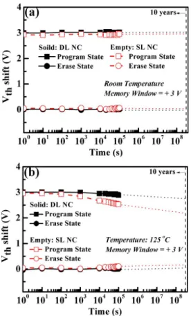
Fig. 4 shows the data retention characteristics of the TANOS memories with an embedded SL and IB-induced DL Ni NCs at room temperature (RT) and 125 °C, respectively. At RT, they both show stable data retention properties without any apparent change in memory window, as shown in Fig. 4(a). As the test temperature is increased to 125 °C, the SL Ni NC sample shows ordinary high-temperature retention properties with a 33% charge loss at extrapolation up to 10 years, as shown in Fig. 4(b). By contrast, the IB-induced DL Ni NC device exhibits better high-temperature retention properties with an only 9% charge loss at extrapolation up to 10 years at 125 °C. This improvement in data retention is attributed to the coulomb blockade effects between TL and BL NCs [17], [31]. As stored in the TL NC, charges are prevented from leaking out at high temperature by the coulomb repulsion effects of charges stored in the BL NC. On the other hand, previous reports indicated that the data retention characteristics of DL metal NC memory and the thickness of the interlayer between TL and BL NCs are closely interactive [32]. With decreasing the thickness of the interlayer between TL and BL NCs, the charge retention capability of DL metal NC memory is degraded. It is easy for charge stored in the TL NC to leak to BL NC via an ultrathin interlayer between TL and BL NCs. Even so, the IB-induced DL Ni NC device with the ultrathin interlayer still shows good data retention properties by comparison with other DL metal NC memories fabricated by general method [16]–[21]. This is attributed to the high-quality interlayer of the IB-induced
Fig. 4. Data retention characteristics of the TANOS memories with embedded SL and IB-induced DL Ni NCs at (a) RT and (b) 125 °C, respectively. As to the data retention measurement, the devices were initially tested at program state, that was, Vth–initial Vth= 3 V.
DL Ni NC. For the IB-induced DL metal NC, it employs the original bottom dielectric as the interlayer. For DL metal NC formed by the conventional method [18]–[21], however, the interlayer is obtained by an additional CVD process, as shown in Fig. 1. The heteromaterial deposition processes easily cause a large number of natural shallow deficiencies around the interface between two kinds of materials. After formation of DL metal NC, a large number of shallow defects exist around the interlayer. This would cause serious charge loss problems, especially in high-temperature environment [27]–[29]. This implies the interlayer quality of the conventional DL metal NC is difficultly controlled. As can be observed easily, the interlayer quality of the IB-induced DL metal NC is certainly better than that of the conventional DL Ni NC. This also explains that why the IB-induced DL Ni NC memory can has such good retention properties, although the interlayer is ultrathin. According to the above results, it is confirmed that the IB-induced DL Ni NC memory possesses wide memory window as well as strong data retention characteristics. For this reason, the IB-induced DL Ni NC memory should be suitable to be applied to multilevel operation. Fig. 5 shows the multilevel-operation data retention characteristics of the TANOS memories with embedded SL and IB-induced DL Ni NCs at 125 °C. For the SL Ni NC sample, a 23% memory narrowing is found at 125 °C for 104 s. By contrast, the IB-induced DL Ni NC device exhibits great multilevel data retention properties with an only 11% change in memory
Fig. 5. Multilevel data retention characteristics of the TANOS memories with embedded SL and IB-induced DL Ni NCs at 125 °C.
Fig. 6. Endurance characteristics of the TANOS memories with embedded SL and IB-induced DL Ni NCs. The conditions of programming and erasing were (VP = 16 V at 100 µs, VE = −17 V at 1 ms) and (VP = 15 V at 100 µs, VE = −16 V at 1 ms) for the SL and IB-induced DL Ni NCs devices, respectively.
window at 125 °C for 104 s. This demonstrates that the IB-induced DL metal NC memory has good potential for multilevel storage. This good potential is attributed to the high-quality ultrathin interlayer between TL and BL NCs induced by the IB technique.
Fig. 6 shows the endurance characteristics of the TANOS memories with embedded SL and IB-induced DL Ni NCs. For the SL Ni NC sample, it is observed that the memory window is seriously degraded after 105 P/E cycles with a 39% narrowing. The shifts of Vth in erase and program states are, respectively, dominated by different physical mechanisms. The upward shift of Vth in erase state is due to NC-induced strong coupling of conduction path [27]. After frequent P/E cycles, it is easy for injection charge to be trapped around the top dielectric due to the NC-induced strong coupling of conduction path. It is difficult for charge stored around the top dielectric to be removed during erasing operation. On the other hand, the downward shift of Vth in program state is ascribed to the damage of the dielectric between BL NC and Si-sub caused by frequent P/E cycles [27]. This damage results in immediate charge losses during pro-gramming process. By contrast, the IB-induced DL Ni NC device exhibits better endurance properties with no apparent
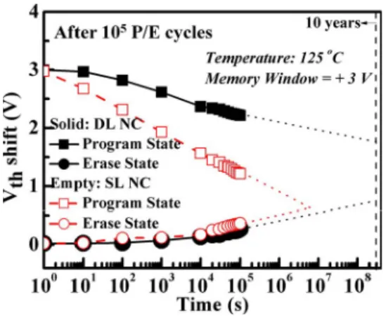
Fig. 7. Postcycled data retention characteristics of the TANOS memories with embedded SL and IB-induced DL Ni NCs at 125 °C. As to the postcycled data retention measurement, the devices were initially tested at program state, that was, Vth–initial Vth= 3 V.
memory window narrowing. This improvement in endurance is attributed to the increase on P/E efficiency and data retention capability. The high P/E efficiency decreases programming and erasing operation voltages to significantly reduce the damage caused by frequent P/E cycles. The excellent data retention suppresses the immediate charge losses. For the IB-induced DL Ni NC device, furthermore, the upward shifts of Vth in erase and program states are both ascribed to the DL metal NC-induced strong coupling of conduction path. Using a decrease of program voltage, however, the upward shifts of Vth can be suppressed. On the other hand, it is found that the IB-induced DL Ni NC device shows the roughly same endurance properties as other DL metal NC memories fabricated by general method [18]. It is worth noting, in contrast to other DL metal NC memories fabricated by general method, the IB-induced DL metal NC device can use relatively low operation voltages to P/E memory window due to the IB-induced ultrathin interlayer between TL and BL NCs. The low operation voltage can significantly decrease the P/E cycles-induced damage and suppress the upward shifts of Vth to improve endurance characteristics. Fig. 7 shows the postcy-cled data retention of the TANOS memories with embedded SL and IB-induced DL Ni NCs at 125 °C. As can be observed, the SL Ni NC sample shows disappointing postcycled data retention properties at 125 °C. The memory window of the SL Ni NC sample is extrapolated to near zero at 6× 10⁶s. The P/E cycles-induced damage and external thermal energy cause fast charge losses. Compared with the SL Ni NC sample, the IB-induced DL Ni NC device exhibits better postcycled high-temperature retention properties. After 105P/E cycles, a 1 V memory window is still maintained at extrapolation up to 10 years at 125 °C. This demonstrates again that the IB-induced DL Ni NC memory has excellent reliability characteristics. On the other hand, the IB-induced DL Ni NC device shows the best postcycled high-temperature retention properties than other multilayer Ni-based NC memories [19], [31]. This is also attributed to the IB-induced high-quality ultrathin interlayer.
Due to an array of arrangements in the practicalNAND-type memory design, a continuous stress on a device may influence the states of surrounding devices [30]. However, so far the related studies have been lacking for DL metal NC memory.
Fig. 8. Program disturbance characteristics of the TANOS memories with embedded SL and IB-induced DL Ni NCs.
To ensure the devices’ reliability, therefore, the disturbance phenomena have to be investigated. Fig. 8 shows the program disturbance characteristics of the TANOS memories with an embedded SL and IB-induced DL Ni NCs. For the SL and IB-induced DL Ni NCs memories, the shifts of Vth on the program disturbance are both< 0.1 V under Vdisturb= 16 V for 103s. As can be observed easily, the program disturbance can be ignored for this IB-induced DL Ni NC memory.
IV. CONCLUSION
The TANOS memory with an embedded IB-induced DL Ni NC has been successfully fabricated and investigated. Compared with the control sample, the SL Ni NC memory, the IB-induced DL Ni NC device exhibits superior electrical characteristics in terms of faster P/E speeds, larger memory window, more stable data retention, and better endurance properties. These improvements in performance are attributed to the 3-D arrangement of DL Ni NC. Additionally, the IB-induced DL Ni NC memory also demonstrates great poten-tial for multilevel operation and high resistance to program disturbance. In contrast to other methods of forming DL metal NC, the IB technique is a relatively simple fabrication method and completely compatible with the current IC manufacturing technologies. Using the IB technique, complex and high-cost processes can be avoided. The IB-induced DL Ni NC memory can combine the properties of high P/E efficiency and excellent reliability simultaneously due to the high-quality ultrathin interlayer between TL and BL NCs. For the conventional fabrication method of DL metal NC, it is difficult for a high-quality ultrathin interlayer to be achieved and controlled. On the contrary, using the IB technique, a high-quality ultra-thin interlayer can be easily formed and controlled owing to elimination of the additional CVD deposition. This is why the IB-induced DL Ni NC device reveals higher P/E efficiency as well as similar excellent reliability by comparison with other DL metal NC memories fabricated by general method. We believe that the IB-induced metal DL NC is a potential technique to be applied to specific NVM products, such as thin-film transistor flash NVM which the cell size is a minor concern for these devices. In addition, the IB technique could be possible to be integrated to 3-D package technology of through silicon via in the future.
ACKNOWLEDGMENT
The authors would like to thank Nano Device Laboratories for the processing support.
REFERENCES
[1] A. Kolodny, S. T. K. Nieh, B. Eitan, and J. Shappir, “Analysis and mod-eling of floating-gate EEPROM cells,” IEEE Trans. Electron Devices, vol. 33, no. 6, pp. 835–844, Jun. 1986.
[2] S. T. Wang, “Charge retention of floating-gate transistors under applied bias condition,” IEEE Trans. Electron Devices, vol. 27, no. 1, pp. 297–299, Jan. 1980.
[3] G. Molas, D. Deleruyelle, B. D. Salvo, G. Ghibaudo, M. Gely, L. Perniola, D. Lafond, and S. Deleonibus, “Degradation of floating-gate memory reliability by few electron phenomena,” IEEE Trans. Electron Devices, vol. 53, no. 10, pp. 2610–2619, Oct. 2006.
[4] R. Shirota, Y. Sakamoto, H. M. Hsueh, J. M. Jaw, W. C. Chao, C. M. Chao, S. F. Yang, and H. Arakawa, “Analysis of the correlation between the programmed and threshold-voltage distribution spread of NAND flash memory device and floating-gate impurity concentra-tion,” IEEE Trans. Electron Devices, vol. 58, no. 11, pp. 3712–3719, Nov. 2011.
[5] M. F. Beug, N. Chan, T. Hoehr, L. M. Meskamp, and M. Specht, “Inves-tigation of program saturation in scaled interpoly dielectric floating-gate memory devices,” IEEE Trans. Electron Devices, vol. 56, no. 8, pp. 1698–1704, Aug. 2009.
[6] S. Mahapatra, S. Shukuri, and J. Bude, “CHISEL flash EEPROM— Part I: Performance and scaling,” IEEE Trans. Electron Devices, vol. 49, no. 7, pp. 1296–1301, Jul. 2002.
[7] G. Zhang, X. P. Wang, W. J. Yoo, and M. F. Li, “Spatial distribution of charge traps in a SONOS-type flash memory using a high-k trapping layer,” IEEE Trans. Electron Devices, vol. 54, no. 12, pp. 3317–3324, Dec. 2007.
[8] Y. N. Tan, W. K. Chim, W. K. Choi, M. S. Joo, and B. J. Cho, “Hafnium aluminum oxide as charge storage layer and blocking-oxide layers in SONOS-type nonvolatile memory for high-speed operation,” IEEE Trans. Electron Devices, vol. 53, no. 4, pp. 654–662, Apr. 2006. [9] X. Wang and D. L. Kwong, “A novel high-k SONOS memory using TaN/Al2O3/Ta2O5/HfO2/Si structure for fast speed and long retention operation,” IEEE Trans. Electron Devices, vol. 53, no. 1, pp. 78–82, Jan. 2006.
[10] T. Y. Chiang, Y. H. Wu, W. C. Y. Ma, P. Y. Kuo, K. T. Wang, C. C. Liao, C. R. Yeh, W. L. Yang, and T. S. Chao, “Characteristics of SONOS-type flash memory with in-situ embedded silicon nanocrystals,” IEEE Trans. Electron Devices, vol. 57, no. 8, pp. 1895–1902, Aug. 2010.
[11] D. W. Kim, T. Kim, and S. K. Banerjee, “Memory characteriza-tion of SiGe quantum dot flash memories with HfO2 and SiO2 tunneling dielectrics,” IEEE Trans. Electron Devices, vol. 50, no. 9, pp. 1823–1829, Sep. 2003.
[12] J. H. Chen, Y. Q. Wang, W. J. Yoo, Y. C. Yeo, G. Samudra, D. S. Chan, A. Y. Du, and D. L. Kwong, “Nonvolatile flash memory device using Ge nanocrystals embedded in HfAlO high-k tunneling and control oxides: Device fabrication and electrical performance,” IEEE Trans. Electron Devices, vol. 51, no. 11, pp. 1840–1848, Nov. 2004.
[13] J. J. Lee and D. L. Kwong, “Metal nanocrystal memory with high-k tunneling barrier for improved data retention,” IEEE Trans. Electron Devices, vol. 52, no. 4, pp. 507–511, Apr. 2005.
[14] Z. Liu, C. Lee, V. Narayanan, G. Pei, and E. C. Kan, “Metal nanocrystal memories–Part I: Device design and fabrication,” IEEE Trans. Electron Devices, vol. 49, no. 9, pp. 1606–1613, Sep. 2002.
[15] Z. Liu, C. Lee, V. Narayanan, G. Pei, and E. C. Kan, “Metal nanocrystal memories—Part I: Electrical characteristics,” IEEE Trans. Electron Devices, vol. 49, no. 9, pp. 1614–1622, Sep. 2002.
[16] Q. Hu, T. K. Eom, S. H. Kim, H. J. Kim, H. H. Lee, Y. S. Kim, D. Y. Ryu, K. B. Kim, and T. S. Yoon, “Vertically and laterally self-aligned double layer of nanocrystals in nanopatterned dielectric layer for nanocrystal floating gate memory device,” Electrochem. Solid-State Lett., vol. 13, no. 11, pp. H366–H369, Aug. 2010.
[17] F. M. Yang, T. C. Chang, P. T. Liu, P. H. Yeh, U. S. Cheng, Y. C. Yu, J. Y. Lin, S. M. Sze, and J. C. Lou, “Using double layer CoSi2 nanocrystals to improve the memory effects of nonvolatile memory devices,” Appl. Phys. Lett., vol. 90, no. 21, pp. 212108-1–212108-3, May 2007.
[18] P. K. Singh, G. Bisht, K. Auluck, M. Sivatheja, R. Hofmann, K. K. Singh, and S. Mahapatra, “Performance and reliability study of single-layer and dual-layer platinum nanocrystal flash memory devices under NAND operation,” IEEE Trans. Electron Devices, vol. 57, no. 8, pp. 1829–1837, Aug. 2010.
[19] S. W. Ryu, J. W. Lee, J. W. Han, S. Kim, and Y. K. Choi, “Designed workfunction engineering of double-stacked metal nanocrystals for nonvolatile memory application,” IEEE Trans. Electron Devices, vol. 56, no. 3, pp. 377–382, Mar. 2009.
[20] P. K. Singh, G. Bisht, R. Hofmann, K. Singh, N. Krishna, and S. Mahapatra, “Metal nanocrystal memory with Pt single-and dual-layer NC with low-leakage Al2O3blocking dielectric,” IEEE Electron Device
Lett., vol. 29, no. 12, pp. 1389–1391, Dec. 2008.
[21] S. K. Samanta, P. K. Singh, W. J. Yoo, G. Samudra, Y. C. Yeo, L. K. Bera, and N. Balasubramanian, “Enhancement of memory window in short channel non-volatile memory devices using double layer tung-sten nanocrystals,” in IEEE IEDM Tech. Dig., Dec. 2005, pp. 170–173. [22] D. B. Farmer and R. G. Gordon, “High density Ru nanocrystal deposition for nonvolatile memory applications,” J. Appl. Phys., vol. 101, no. 12, pp. 124503-1–124503-5, Jun. 2007.
[23] C. H. Chen, T. C. Chang, I. H. Liao, P. B. Xi, C. T. Tsai, P. Y. Yang, J. Hsieh, J. Chen, U. S. Cheng, and J. R. Cheng, “Tungsten nanocrystal memory devices improved by using supercritical fluid treatment,” Appl. Phys. Lett., vol. 91, no. 23, pp. 232104-1–232104-3, Dec. 2007. [24] K. S. Seol, S. J. Choi, J. Y. Choi, E. J. Jang, B. K. Kim, S. J. Park,
D. G. Cha, I. Y. Song, J. B. Park, and S. H. Choi, “Pd-nanocrystal-based nonvolatile memory structure with asymmetric SiO2/HfO2tunnel barrier,” Appl. Phys. Lett., vol. 89, no. 8, pp. 083109-1–083109-3, Aug. 2006.
[25] C. Cabral, J. Kedzierski, B. Linder, S. Zafar, V. Narayanan, S. Fang, A. Steegen, P. Kozlowski, R. Carruthers, and R. Jammy, “Dual work-function fully silicided metal gates,” in Symp. VLSI Technol. Tech. Dig., Jun. 2004, pp. 184–185.
[26] J. J. Lee, Y. Harada, J. W. Pyun, and D. L. Kwong, “Nickel nanocrystal formation on HfO2 dielectric for nonvolatile memory device appli-cations,” Appl. Phys. Lett., vol. 86, no. 10, pp. 103505-1–103505-3, Mar. 2005.
[27] S. H. Liu, W. L. Yang, Y. P. Hsiao, and T. S. Chao, “Robust data retention and superior endurance of silicon–oxide–nitride–oxide–silicon-type nonvolatile memory with NH3-plasma-treated and Pd-nanocrystal-embedded charge storage layer,” Jpn. J. Appl. Phys., vol. 51, no. 4, pp. 04DD05-1–04DD05-4, Apr. 2012.
[28] C. C. Lin, T. C. Chang, C. H. Tu, W. R. Chen, C. W. Hu, S. M. Sze, T. Y. Tseng, S. C. Chen, and J. Y. Lin, “Improved reliability of Mo nanocrystal memory with ammonia plasma treatment,” Appl. Phys. Lett., vol. 94, no. 6, pp. 062106-1–062106-3, Feb. 2009.
[29] T. K. Kang, T. C. Liao, C. L. Lin, and W. F. Wu, “Effect of nitro-gen plasma treatment on electrical characteristics for Pd nanocrys-tals in nonvolatile memory,” Jpn. J. Appl. Phys., vol. 49, no. 8, pp. 086202-1–086202-5, Aug. 2010.
[30] S. H. Liu, W. L. Yang, C. C. Wu, and T. S. Chao, “A novel ion-bombarded and plasma-passivated charge storage layer for SONOS-type nonvolatile memory,” IEEE Electron Device Lett., vol. 33, no. 10, pp. 1393–1395, Oct. 2012.
[31] W. R. Chen, T. C. Chang, J. L. Yeh, S. M. Sze, and C. Y. Chang, “Formation and nonvolatile memory characteristics of multilayer nickel-silicide NCs embedded in nitride layer,” J. Appl. Phys., vol. 104, no. 9, pp. 094303-1–094303-6, Nov. 2008.
[32] S. W. Ryu, Y. K. Choi, C. B. Mo, S. H. Hong, P. K. Park, and S. W. Kang, “A thickness modulation effect of HfO2 interfacial layer between double-stacked Ag nanocrystals for nonvolatile memory device applications,” J. Appl. Phys., vol. 101, no. 2, pp. 026109-1–026109-3, Jan. 2007.
Sheng-Hsien Liu received the B.S. degree in electronic engineering from Feng Chia University, Taichung, Taiwan, in 2007, where he is currently pursuing the Ph.D. degree in the Ph.D. Program of Electrical and Communications Engineering.
versity, Hsinchu, Taiwan, in 2006.
He is currently an Associate Professor with National United University, Miaoli, Taiwan.
University, Hsinchu, Taiwan, in 1992.
He is currently a Professor with National Chiao-Tung University.