A Filtering Microstrip Antenna Array
Chin-Kai Lin and Shyh-Jong Chung, Senior Member, IEEE
Abstract—A new filtering microstrip antenna array is presented.
The antenna elements, together with the very compact feeding work, function as a third-order bandpass filter. The feeding net-work, which consists of one power divider and two baluns, vides the first two stages, and the microstrip antenna elements pro-vide the last stage in the filter design. The equivalent lumped cir-cuit model is analyzed, and the detail synthesis procedure is pre-sented. A third-order filtering 2 2 microstrip antenna array is designed at a center frequency of 5 GHz with 3% fractional band-width and Chebyshev 0.3-dB equal-ripple broadside antenna gain response. The results from circuit model, full-wave simulation, and measurements agree well. Compared to the conventional patch an-tenna array, the proposed filtering microstrip anan-tenna array suc-cessfully suppresses the unwanted signals in out-of-band, preserves good selectivity at band edges, and retains the flatness of the pass-band broadside antenna gain response.
Index Terms—Balun, bandpass filter (BPF), filtering antenna,
microstrip antenna array, power divider.
I. INTRODUCTION
A
S THE development of wireless communication tech-nologies grows rapidly, integration among components has become a significant issue. In a wireless communication system, the antenna is an essential component for receiving and transmitting signals, while the bandpass filter (BPF) is another crucial component for selecting signals in the required band and rejecting the unwanted signals. Generally, a BPF is composed of resonators with the same resonant frequency as the antenna so it leads to interferences on the return loss and the antenna gain responses, especially at the band edges. Usually the impedance bandwidth of the antenna is different from that of the BPF. The I/O ports of a BPF are typically designed for 50- terminations. However, the input impedance of the antenna may not be perfectly matched to 50 at the band edges. The degradation due to mismatch thus occurs. Since both of these components are generally arranged at the very front-end of a communication system, integration of the antenna and the BPF is considered for enhancing the overall performance and reducing circuit area.Recently, quite a few antennas in different forms were de-signed through the filter synthesis process, in which the antenna acts as one of the resonators in the filter design. Coupled circular Manuscript received April 21, 2011; accepted May 02, 2011. Date of publi-cation August 04, 2011; date of current version November 16, 2011. This work was supported in part by the National Science Council, R.O.C., under Contract NSC 97-2221-E-009-041-MY3.
The authors are with the Institute of Communications Engineering, National Chiao Tung University, Hsinchu 300, Taiwan (e-mail: [email protected]. tw).
Color versions of one or more of the figures in this paper are available online at http://ieeexplore.ieee.org.
Digital Object Identifier 10.1109/TMTT.2011.2160986
patches were introduced for multiple mode operation in [1]–[4]. Several antennas in different forms, such as slot dipole antennas [5], [6], monopole antennas [7], microstrip antennas [8]–[11], and substrate integrated waveguide (SIW) slot antennas [12] are also integrated with BPFs.
Additionally, over the last few decades, the microstrip an-tenna array has become one of the most popular candidates for highly directive antenna applications because of its characteris-tics of low profile, light weight, low cost, and easy fabrication. For the requirement of high directivity, the number of antenna elements tends to increase, and the feeding network must be more complicated. As the feeding network becomes complex, some unexpected resonances occur and result in spurious pass-bands at unwanted frequencies. Intuitively, the spurious signals can be suppressed by a BPF placed right after the antenna array. However, as mentioned previously, a BPF interacts with the an-tenna array and degrades the performance, especially at the band edges. In order to solve this dilemma, one of the possible solu-tions is to replace the antenna elements by the filtering antennas [8]–[11]. If antenna elements act as the first/last stage of the receiver/transmitter have the filtering function, then the signals received/transmitted by the system will no longer be interfered by the noises in unwanted bands.
Traditionally, the feeding network of the antenna array only has the function of transmitting the signals with proper magnitudes and phases to the antenna elements. The feeding network is usually a combination of transmission lines, power dividers, and baluns (balanced-to-unbalanced transformers). Therefore, the filtering power dividers [13] and the filtering baluns [14]–[16] utilizing coupled resonators can be applied for designing the feeding network so that the feeding network has both the functions of power division and band selection.
In this paper, we go a step further by combining the filtering antenna elements and the filtering feeding network so that the circuitry has the return loss and the antenna gain response just like a BPF. A 2 2 antenna array is implemented with a third-order Chebyshev BPF response. Functioning as the last stage of the filter, the radiating patch in [11] is adopted for the array el-ements, while the feeding network contributes to the first two stages. This paper is organized as follows. Section II illustrates the layout and the equivalent lumped circuit of the filtering mi-crostrip antenna array. Section III describes the design proce-dure and exhibits the simulation results. Section IV presents the comparison between the proposed filtering microstrip antenna array and nonintegrated conventional patch antenna array with BPF. Section V shows the measured results and is followed by conclusions in Section VI.
II. STRUCTURE ANDEQUIVALENTCIRCUIT
The layout, components, and equivalent circuit of the pro-posed filtering microstrip antenna array are investigated in this 0018-9480/$26.00 © 2011 IEEE
TABLE I
THIRD-ORDERCHEBYSHEVFILTERPROTOTYPESPECIFICATIONS
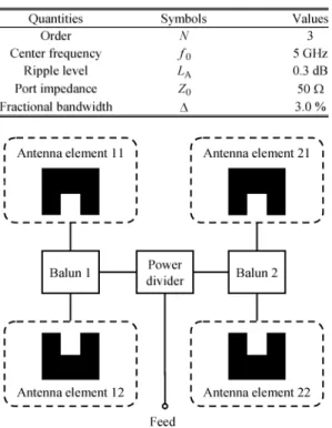
Fig. 1. Functional block diagram of the filtering micristrip antenna array.
section. This design is at a center frequency of 5 GHz, with third-order Chebyshev equal-ripple broadside antenna gain response, 0.3-dB ripple level, 3% fractional bandwidth, and 50- port impedance. The BPF specifications are summarized in Table I.
A. Topology of the Filtering Microstrip Antenna Array
The functional block diagram of the filtering microstrip an-tenna is illustrated in Fig. 1. At the four corners, four array el-ements are placed a half free-space wavelength apart from the adjacent ones for minimizing sidelobes. For focusing the main beam in the broadside direction, the feeding network need to be properly designed so that the signals on these four antenna ele-ments are synchronized [17]. The antenna eleele-ments 11 and 12 are arranged back to each other for saving the circuit area and reducing the layout complexity. Linked by a balanced- to-un-balanced transformer (balun 1), the antenna elements 11 and 12 have the same phase. The same applies to antenna elements 21 and 22. In order to connect baluns 1 and 2, a power divider is placed at the center to equally split the signal into these two baluns, while the input port of the power divider is connected to the antenna array feeding point.
The physical layout of the proposed filtering microstrip an-tenna array is depicted in Fig. 2. It is printed on a piece of RT/Duroid 5880 substrate with a dielectric constant of 2.2 and a thickness of 0.508 mm. The filtering microstrip antenna array consists of four parts: four radiating patches, two vertical half-wavelength resonators, one inverted E-shape resonator, and one section of feeding microstrip line with the interdigital coupler.
At the bottom of Fig. 2 is a 50- microstrip feed line of width . At the top end of the feed line is the interdigital coupler for
Fig. 2. Topology of the filtering microstrip antenna array.
feeding the first stage, the E-shape resonator. The E-shape res-onator is essentially a half-wavelength resres-onator;
is about half a guiding wavelength. At the sides next to the E-shape resonator, there are two vertical half-wavelength res-onators, which act as the second-stage resonators. Since the ge-ometry is symmetrical, the couplings for these two half-wave-length resonators are equal. Thus, the first- and second-stage resonators together can be treated as an power and equal-phase power divider, which corresponds to the power divider in Fig. 1.
Observing the left-hand side of Fig. 2, the half-wavelength resonator and two radiating patches are all operated at their fun-damental modes at the same resonant frequency, . Around the resonant frequency, suppose that at some instance in one pe-riod, the current flows on the half-wavelength resonator in the -direction. Through the gap coupling, the current induced on the radiating patches must be in -direction as well, but with 90 phase difference to the current of the half-wavelength res-onator. However, the currents on these two radiating patches are synchronized. Thus, they radiate coherently in broadside ( -) direction. These are the baluns in Fig. 1, which is the similar operation principle inspired by [14]–[16].
On the four corners of Fig. 2, there are four radiating patches as the array elements. The element spacings, and , are both approximately a half free-space wavelength. During the design process, we treat them as the last-stage resonators with loads since they resonate at and dissipate the electromagnetic power into the air.
B. Equivalent Third-Order BPF Model
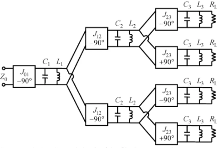
Since the filtering microstrip antenna array is composed of coupled resonators, the equivalent circuit in Fig. 3 is con-structed accordingly. All the resonators in Fig. 2 are modeled by shunt resonators with the same resonant frequency, . The E-shape resonator, the half-wavelength resonators, and the
Fig. 3. Equivalent lumped circuit of the filtering microstrip antenna array.
TABLE II
CORRESPONDENCESAMONGFIGURES
radiating patches are, respectively, modeled by , , and resonators [17], [18].
The coupling gaps between the resonators are modeled by mittance inverters. The interdigital coupler is modeled by an ad-mittance inverter . The coupling between the first and second stages is expressed by two admittance inverters with iden-tical 90 phase delay. As for the four gaps between the second and third stages, two of them are modeled by a pair of admit-tance inverters with 90 phase delay, and the other two are with 90 phase delay. The 180 phase difference among the paired radiating patches are functioning as the baluns. The cor-respondences among Figs. 1–3 are summarized in Table II.
All of the parameters of the equivalent lumped circuit in Fig. 3 can be calculated utilizing the BPF synthesis technology [18]
(1) arbitrary (2) arbitrary (3) (4) (5) (6) (7) (8)
where , , , and are the normalized Chebyshev low-pass filter prototype element values, which are functions of the ripple level . Although and have arbitrary values, the first-stage external quality factor and the coupling coefficients between stages ( and ) are not affected [18]
(9) (10) (11) Note that in (11) and (12), the admittance inverter is slightly different from the ones in conventional filter synthesis. Since power is split into two, the values of the admittance inverters are divided by .
III. DESIGN
The synthesis of a filtering microstrip antenna array is pre-sented in this section. The filtering microstrip antenna array is deconstructed into several parts, which are designed individu-ally.
By looking up tables in the literature [18], the normalized Chebyshev low-pass filter prototype element values with the
ripple level of dB are , ,
and . Applying (1)–(11) with the filter specifications given in Table I, the values that we need for parameter
extrac-tions are ,
pF, and pH.
The synthesis of the filtering microstrip antenna array is dif-ferent from the conventional filter synthesis technologies be-cause the load, or the impedance of port 2 in the filter termi-nology, cannot be separated from the radiating patch. Therefore, the parameter extractions of the radiating patch, such as external quality factors and the coupling coefficients, are quite different. We are forced to rely more on the lumped circuit model. In the following, the design process will be discussed in detail. The full-wave simulation throughout this work is done using IE3D [19].
A. External Quality Factor of the First-Stage Resonator
Fig. 4 is plotted for designing the feed of the first-stage onator and the coupling between the first- and second-stage res-onators. Fig. 4(a) is the test structure for extracting the external quality factor of the first stage. The thin microstrip section with width at the center of the E-shape resonator is for enhancing the coupling with the interdigital coupler [20]. As previously
mentioned, is about half a guiding
wave-length. The dimensions of the E-shape resonator and interdigital coupler in Fig. 4(a) are listed in the figure caption. The coupling gap is the tuning variable for the required external quality
factor [18]
Fig. 4. Q and M extractions. (a) Test structure for the first-stage external quality factorQ . The physical dimensions are: w = 1:15 mm, w = 0:3 mm, l = 0:7 mm, l = 28:1 mm, and l = 5:625 mm, while the gap g is the tuning variable. (b) Test structure for the coupling coefficient M . The physical dimensions are:w = 1:15 mm, l = 21:3 mm, w = 0:3 mm, l = 0:7 mm, l = 28:1 mm, and l = 5:625 mm, while the gap g is the tuning variable. (c)Q and M as the functions of g and g , respectively.
where is the resonant frequency and is the frequency difference between 90 and 90 of the reflection coefficient. The full-wave simulated is a function of and is plotted in Fig. 4(c). As calculated previously, the required . Thus, mm is chosen for the precise coupling.
B. Coupling Coefficient of the First Two-Stage Resonators
Fig. 4(b) is the structure for testing the coupling between the first two-stage resonators. The first-stage E-shape resonator was already designed in Section III-A. Two 50- half-wavelength resonators with length and width are symmetrically placed besides the E-shape resonator with a gap size . The dimen-sions of the structure in Fig. 4(b) are listed in the figure caption. Using the conventional technique for extracting the coupling between resonators [18], by recording two resonant frequencies of the coupled-resonator structure in Fig. 4(b), and , then the coupling coefficient between the two resonators, , can be calculated
(13) By adjusting the gap size , we can get the proper coupling level. The full-wave simulated as a function of is plotted (the dashed line) in Fig. 4(c). As calculated previously, the required and the corresponding gap size
Fig. 5. Radiating patch extraction. (a) Structure under test. (b) Equivalent lumped circuit. (c) Input impedance responses of the full-wave simulated struc-ture and the equivalent lumped circuit with the dimensionsw = 21:0 mm, l = 19:3 mm, s = 5:2 mm, s = 9:95 mm, g = 4:56 mm, l = 10:65 mm, and w = 1:15 mm.
mm should be chosen for the required coupling coefficient.
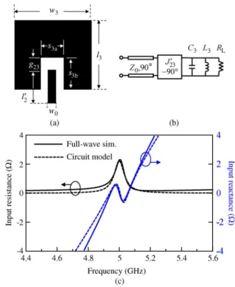
C. Radiating Patch Design
The radiating patch is modeled by the parallel resonator with three parameters, , , and to be determined. Since the radiation resistance of the radiating patch is inseparable from the resonator, the conventional external quality factor extraction method for the last stage of the BPF cannot be applied. Instead, we establish the test structure, as shown in Fig. 5(a), for ex-tracting the element values of the corresponding equivalent cir-cuit of the radiating patch in Fig. 5(b).
In Fig. 5(a), the radiating patch is excited by an inserted quarter-wavelength 50- microstrip line with length , and it is modeled by the resonator in Fig. 5(b). The coupling between the radiating patch and the quarter-wavelength 50-microstrip line is modeled by an admittance inverter . The coupling here is relatively weaker than that in the final design because the coupling section is not in resonance. That is, is a temporary admittance inverter only for testing and is different from in Fig. 3.
These three parameters to be determined corre-spond to resonant frequency, unloaded quality factor, and load of the resonator [17]. The radiating patch is a half-wavelength square with a coupling section. The resonant frequency of a patch is mainly determined by the patch length . The cou-pling structure affects the unloaded quality factor. The width of the patch, , mainly affects the antenna resistance , but the unloaded quality factor is also influenced. While the gap
size varies, the value of varies. However, the coupling strength does not affect the internal parameters of the resonator.
As shown in Fig. 5(c), the parameters are extracted by fit-ting the input impedances of the circuits in Fig. 5(a) and (b). The lumped element values that were calculated previously are
pF, pH, and The
tem-porary admittance inverter mS is obtained by curve fitting. The corresponding dimensions of the radiating patch are listed in the figure caption. From Fig. 5(c), the impedances of the circuit model and full-wave simulation are well fitted.
D. Coupling Between the Last Two-Stage Resonators
Since the radiation resistance of the radiating patch is in-separable from the resonator, once again, the extraction of the coupling between the last two-stage resonators must utilize the equivalent circuit.
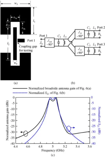
Fig. 6(a) depicts the structure under test (one half-wavelength resonator and two radiating patches), and Fig. 6(b) represents its equivalent circuit. The half-wavelength resonator is modeled by . Two radiating patches are modeled by together with two output ports, port 2 and port 3, with port impedance . The couplings between the last two stages are, respectively, modeled by two admittance inverters, , with 180 phase dif-ference, and a loose input coupling is modeled by another ad-mittance inverter with a very small value of .
For the equivalent circuit in Fig. 6(b), one of the possible combinations for this previously calculated coupling coefficient
is pF, pH,
and mS. The normalized response (dashed line) of the equivalent circuit is plotted in Fig. 6(c).
The physical dimensions of the radiating patches and the half-wavelength resonator in Fig. 6(a) remain the previously
de-signed values: mm, mm, mm,
mm, mm, mm, and
mm. The half-wavelength resonator is excited by a loose coupled input. Our goal here is to adjust the gap to fit the normalized broadside antenna gain response with the normalized response of the equivalent circuit. When mm, as shown in Fig. 6(c), normalized broadside antenna gain response (solid line) fits well with the re-sponse of the equivalent circuit (dashed line).
E. Simulation Results
After the extraction works, the last step is to put all the stages together. The final dimensions for the filtering microstrip
an-tenna in Fig. 2 are mm, mm,
mm, mm, mm, mm,
mm, mm, mm,
mm, mm, mm, and mm.
The element spacing in - and -directions are and mm, respectively.
Fig. 7 shows the results of both the full-wave simulation and the lumped circuit model. The dashed lines represent the reflection and transmission responses of the lumped circuit model, and the solid lines stand for the full-wave simulated reflection coefficient and the broadside antenna gain responses. The broadside antenna gain of the filtering microstrip antenna
Fig. 6. Extraction of the coupling between the last two stages. (a) Test structure. (b) Equivalent lumped circuit. (c) Comparison of normalized broadside gain and the normalizedS responses with the physical dimensions: w = 21:0 mm, l = 19:3 mm, s = 5:2 mm, s = 9:95 mm, g = 4:56 mm, l = 21:3 mm, and w = 1:15 mm, and g = 4:56 mm.
Fig. 7. Simulated reflection coefficients, normalized transmission coefficient, and normalized broadside antenna gain.
array corresponds to the transmission coefficient in the lumped circuit model, in which the antenna resistances, ’s, are acting as the “remote ports.” Both of them are normalized for comparison.
Observing the reflection coefficients, the full-wave simula-tion and the circuit model are in good agreement with minimum
return loss of 11.7 dB and 3% fractional bandwidth in the passband.
The filtering microstrip antenna array is symmetric about the -plane, which is an H-wall. The cross-polarized component of the broadside ( -) direction antenna gain vanishes for all fre-quencies. Thus, the broadside antenna gain is purely co-polar-ized. The maximum value of the co-polarized broadside antenna gain is 9.6 dBi. The out-of-band ( 4.8 and 5.2 GHz) radiation level is 15 dBi or lower. Comparing to the passband antenna gain, a 24-dB rejection is achieved.
Comparing the “broadside antenna gain” and the “transmis-sion mis“transmis-sion coefficient” responses, the “broadside antenna gain” has even better selectivity because of the radiation nulls at 4.8 and 5.2 GHz. At these two frequencies, the current induced on the radiating patches are very weak. The radiations due to the open ends of the resonators cancel out each others’ contributions in the broadside direction. Around 5.08 GHz, the band edge of the broadside gain response is slightly shifted to lower frequency because the radiation null is close to the passband.
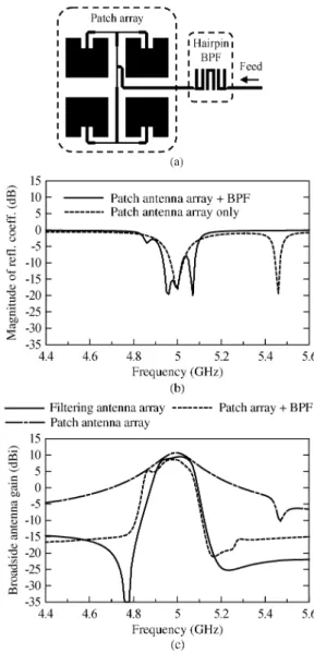
IV. COMPARISONWITH AREGULARPATCHANTENNAARRAY To demonstrate the advantages of the proposed filtering mi-crostrip array, a conventional patch antenna array and a hairpin BPF are cascaded for comparison.
Fig. 8(a) is the topology that printed on the same substrate, RT/Duroid 5880 with dielectric constant 2.2- and 0.508-mm thickness. Four inset patch antennas are placed a half free-space wavelength (about 30 mm) apart from the adjacent ones. The feeding network is now composed of nonresonant transmission lines and T-junctions. The Chyebyshev hairpin BPF is designed with the same as the specifications listed in Table I. The con-ventional patch antenna array and the hairpin BPF are intercon-nected by a section of a 50- microstrip line. The interconnec-tion is not optimized because this is the general scenario when we design an RF front end system—components are bridged by 50- transmission lines with arbitrary lengths.
Fig. 8(b) shows the reflection coefficient of the patch antenna array with and without the hairpin BPF. For the patch antenna array without the BPF (dashed line), there is an unexpected spu-rious radiation at 5.45 GHz. It is caused by the feeding network. This problem can be solved when a BPF is added right after the patch antenna array. However, the antenna resistance is not 50 when the operating frequency is away from its center, while the I/O ports of the BPF are still designed for 50- terminations. The mismatch may lead to the degradation on band-edge se-lectivity. From the result in Fig. 8(b) (solid line), although the spurious signal at 5.45 GHz is eliminated, there comes an ad-ditional resonance at 4.85 GHz due to the interference between the antenna array and the hairpin BPF. In addition, the max-imum return loss in pass band is only 6.5 dB at 5.04 GHz, i.e., the passband impedance matching is also degraded.
One of the best ways to solve this problem is to apply the fil-tering microstrip antenna array. Fig. 8(c) shows the comparison among the broadside antenna gains of several structures. The broadside antenna gain response of the conventional patch an-tenna array (dashed–dotted line) has a maximum gain of 10 dBi at the center frequency, but with a 2.5-dB gain variation in the
Fig. 8. Comparison between the proposed filtering microstrip antenna and the conventional patch antenna array with/without a hairpin BPF. (a) The conven-tional patch antenna array and hairpin BPF. (b) Comparison on simulated re-flection coefficients. (c) Comparison on simulated broadside antenna gains.
passband. For the patch antenna array with the BPF (dashed line), the passband response is seriously affected by the un-wanted couplings, and the gain is rather lower than that of the filter microstrip antenna array. For the proposed filtering mi-crostrip antenna array (solid line), although the peak gain is about 1 dB lower, the gain variation reduces to less than 1 dB, the roll-off of the band-edge is much steeper, and the out-of-band rejection is much stronger.
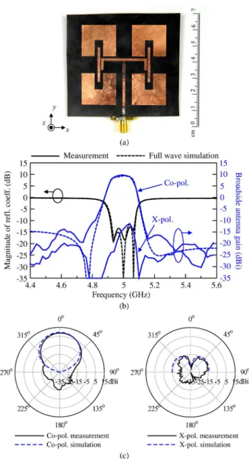
V. MEASUREMENTRESULT
Fig. 9(a)–(c) shows, respectively, the photograph, measured/ simulated results, and -plane radiation patterns of the fabri-cated filtering microstrip antenna array. In Fig. 9(b), the mea-sured magnitude of reflection coefficient has decent agreement with the simulated gain. In the passband, three transmission poles and minimum return loss of 11.7 dB in the passband are observed, as expected.
The measured co-polarized broadside antenna gain also fits well with the simulated results in passband. In the out-of-band
Fig. 9. (a) Photograph of the fabricated filtering microstrip array antenna. (b) Reflection coefficient and broadside antenna gain response. (c) Measured and simulatedH-plane (xz-plane) radiation patterns at 5 GHz.
regions, there are some ripples due to the limitation of the sen-sitivity of the measurement system. However, the out-of-band broadside antenna gain is less than 15 dBi.
As previously mentioned, there is theoretically a cross-polar-ized radiation null in broadside direction because of geometrical symmetry. The measured cross-polarized gain has a maximum level 12 dBi in the passband due to the measurement error. Nonetheless, this is significantly lower than the co-polarized gain, and can be negligible. The measured antenna efficiency at 5 GHz is 72.2%.
The measured and simulated -plane radiation patterns at 5 GHz are plotted in Fig. 9(c). Only the upper plane of the sim-ulated radiation pattern is plotted due to the infinite ground setup in IE3D. The radiation pattern of the filtering microstrip antenna array is similar to that of the regular patch antenna array. The co-polarized radiation pattern has a maximum 9.6-dBi gain in
broadside direction. The simulated 3-dB beamwidth is 46 . The maximum simulated cross-polarized gain resulted from the res-onant structures is about 14 dBi at 45 . Although the mea-sured broadside cross-polarized radiation null is not so obvious, the radiation level is rather low in all directions.
VI. CONCLUSION
This paper has presented a third-order filtering microstrip an-tenna array with a Chebyshev equal-ripple broadside anan-tenna gain response and a pair of antenna nulls beside the passband. Without suffering from any additional circuit area, the antenna elements together with the feeding network own the function of a filter. The detail synthesis procedure and measured results are presented. Comparing to the regular patch antenna array, the proposed filtering microstrip antenna array successfully sup-presses the unexpected spurious signals and retains the flatness of the passband broadside antenna gain response.
REFERENCES
[1] H. Blondeaux, D. Baillargeat, P. Leveque, S. Verdeyme, P. Vaudon, P. Guillon, A. Carlier, and Y. Cailloce, “Microwave device combining and radiating functions for telecommunication satellites,” in IEEE
MTT-S Int. Microw. Symp. Dig., May 2001, pp. 137–140.
[2] H. Blondeaux, D. Baillareat, S. Verdeyme, P. Guillon, A. Carlier, Y. Cailloce, and E. Rogeaux, “Radiant microwave filter for telecommuni-cations using hiQu dielectric resonator,” in Proc. 30th Eur. Microw.
Conf., 2000, pp. 1–4.
[3] I. Hunter, “Broadband matching of antenna using dual-mode radiators,” in Proc. 33rd Eur. Microw. Conf., 2003, pp. 431–434.
[4] A. I. Abunjaileh, I. C. Hunter, and A. H. Kemp, “A circuit-theoretic approach to the design of quadruple-mode broadband microstrip an-tennas,” IEEE Trans. Microw. Theory Tech., vol. 56, no. 4, pp. 896–900, Apr. 2008.
[5] S. Oda, S. Sakaguchi, H. Kanaya, R. K. Pokharel, and K. Yoshida, “Electrically small superconducting antennas with bandpass filters,”
IEEE Trans. Appl. Supercond., vol. 17, no. 2, pp. 878–881, Jun. 2007.
[6] T. E. Nadan, J. P. Coupez, S. Toutain, and C. Person, “Integration of an antenna/filter device, using a multi-layer, multi-technology process,” in
Proc. 28th Eur. Microw. Conf., 1998, pp. 672–677.
[7] C.-T. Chuang and S.-J. Chung, “New printed filtering antenna with se-lectivity enhancement,” in Proc. 39th Eur. Microw. Conf., 2009, pp. 747–750.
[8] T. L. Nadan, J. P. Coupez, S. Toutain, and C. Person, “Optimization and miniaturization of a filter/antenna multi-function module using a composite ceramic-foam substrate,” in IEEE MTT-S Int. Microw. Symp.
Dig., Jun. 1999, pp. 219–222.
[9] A. Abbaspour-Tamijani, J. Rizk, and G. Rebeiz, “Integration of filters and microstrip antennas,” in Proc. IEEE AP-S Int. Symp., Jun. 2002, pp. 874–877.
[10] F. Queudet, I. Pele, B. Froppier, Y. Mahe, and S. Toutain, “Integra-tion of pass-band filters in patch antennas,” in Proc. 32th Eur. Microw.
Conf., 2002, pp. 685–688.
[11] C.-K. Lin and S.-J. Chung, “A compact edge-fed filtering microstrip antenna with 0.2 dB equal-ripple response,” in Proc. 39th Eur. Microw.
Conf., 2009, pp. 378–380.
[12] S. Avrillon, I. Pele, A. Chousseaud, and S. Toutain, “Dual-band power divider based on semiloop stepped-impedance resonators,” IEEE
Trans. Microw. Theory Tech., vol. 51, no. 4, pp. 1269–1273, Apr.
2003.
[13] Y. Yusuf and X. Gong, “A new class of 3-D filter/antenna integration with high quality factor and high efficiency,” in IEEE MTT-S Int.
Mi-crow. Symp. Dig., May 2010, pp. 892–895.
[14] K.-T. Chen and S.-J. Chung, “A novel compact balanced-to-unbal-anced low-temperature co-fired ceramic bandpass filter with three cou-pled lines configuration,” IEEE Trans. Microw. Theory Tech., vol. 56, no. 7, pp. 1714–1720, Jul. 2008.
[15] C.-H. Wu, C.-H. Wang, S.-Y. Chen, and C.-H. Chen, “Balanced-to-unbalanced bandpass filters and the antenna application,” IEEE Trans.
[16] L. K. Yeung and K. L. Wu, “A dual-band coupled-line balun filter,”
IEEE Trans. Microw. Theory Tech., vol. 55, no. 11, pp. 2406–2411,
Nov. 2007.
[17] C. A. Balanis, Antenna Theory, 2nd ed. New York: Wiley, 1997, ch. 14.
[18] J. S. Hong and M. J. Lancaster, Microstrip Filters for RF/Microwave
Applications. New York: Wiley, 2001.
[19] S. W. Wong and L. Zhu, “Implementation of compact UWB bandpass filter with a notch-band,” IEEE Microw. Wireless Compon. Lett., vol. 18, no. 1, pp. 10–12, Jan. 2008.
[20] IE3D Simulator. Zeland Softw. Inc., Fremont, CA, Jan. 1997.
Chin-Kai Lin was born in Keelung, Taiwan. He
received the B.S. and M.S. degree in physics from National Tsing Hua University, Hsinchu, Taiwan, in 2004 and 2006, respectively, and is currently working toward the Ph.D. degree in communication engineering at National Chiao Tung University, Hsinchu, Taiwan.
His current research interests include the design of antennas and microwave circuits.
Shyh-Jong Chung (M’92–SM’06) was born in
Taipei, Taiwan. He received the B.S.E.E. and Ph.D. degrees from National Taiwan University, Taipei, Taiwan, in 1984 and 1988, respectively.
Since 1988, he has been with the Department of Communication Engineering, National Chiao Tung University, Hsinchu, Taiwan, where he is currently a Professor. From September 1995 to August 1996, he was a Visiting Scholar with the Department of Elec-trical Engineering, Texas, A&M University, College Station. His areas of interest include the design and applications of active and passive planar antennas, low-temperature co-fired ce-ramic (LTCC)-based RF components and modules, packaging effects of mi-crowave circuits, vehicle collision warning radars, and communications in in-telligent transportation systems (ITSs).
Dr. Chung was the treasurer of the IEEE Taipei Section (2001–2003) and the chairman of the IEEE Microwave Theory and Techniques Society (IEEE MTT-S) Taipei Chapter (2005–2006). He was the recipient of the Outstanding Electrical Engineering Professor Award of the Chinese Institute of Electrical Engineering and the Teaching Excellence Awards of the National Chiao Tung University (both in 2005).