Enhanced Extraction and Efficiency of Blue Light-Emitting
Diodes Prepared Using Two-Step-Etched Patterned
Sapphire Substrates
Ray-Ming Lin,a,b,
*
,zYuan-Chieh Lu,aSheng-Fu Yu,cYewChung Sermon Wu,d Chung-Hao Chiang,a Wen-Ching Hsu,eand Shoou-Jinn Changc,*
a
Department of Electronic Engineering and bGreen Research Technology Center, Chang-Gung University, Taoyuan 333, Taiwan
c
Institute of Microelectronics and Department of Electrical Engineering, Center for Micro/Nano Science and Technology Advanced Optoelectronic Technology Center, National Cheng-Kung University, Tainan 70101, Taiwan
d
Department of Materials Science and Engineering, National Chiao-Tung University, Hsinchu 300, Taiwan e
Sino-American Silicon Products Incorporated, Hsinchu 300, Taiwan
Using a hot acid wet etching method, we have fabricated two types of patterned sapphire substrates: A pyramidal patterned sapphire substrate共PPSS兲 and a flat-top patterned sapphire substrate 共FTPSS兲. After placing these samples into an atmospheric pressure metallorganic chemical vapor deposition system, we deposited standard InGaN light-emitting diode共LED兲 structures onto their surfaces. The crystal quality of these two surfaces was enhanced, as evidenced using X-ray diffraction共the full width at half-maximum decreased from 406.8 arcsec for the conventional sapphire to 356.4 and 349.2 arcsec for the PPSS and FTPSS samples, respectively兲. The output power of InGaN-based blue LEDs incorporating the PPSS and FTPSS improved to 17.9 and 18.7%, respectively, at 20 mA.
© 2009 The Electrochemical Society. 关DOI: 10.1149/1.3231502兴 All rights reserved.
Manuscript submitted May 26, 2009; revised manuscript received August 3, 2009. Published October 1, 2009.
Gallium nitride共GaN兲-based light-emitting diodes 共LEDs兲 have attracted much attention in recent years because of their high per-formance and promising reliability.1,2They are also considered to be one of the best candidates for replacing conventional incandescent and fluorescent lamps. Many commercial applications of GaN-based LEDs have been realized: e.g., traffic signals, large-scale full-color outdoor displays, backlighting of liquid crystal displays, and cell phones. Although GaN-based LEDs have great potential for use in solid-state lighting, the output efficiency remains limited because of many dislocations within the structures that result from the large lattice mismatch and the different thermal expansion coefficients of the sapphire substrate and GaN. Because the threading dislocation density共TDD兲 is usually ca. 107–109 cm−2in a grown GaN film,3
GaN LEDs usually exhibit greatly reduced internal quantum effi-ciencies共IQEs兲.
Epitaxial lateral overgrowth共ELOG兲 is one method proposed to overcome the problem of dislocation in GaN epitaxial films.4-6First, a thin GaN buffer layer is grown on top of the sapphire substrate, and then a striped SiO2 mask is deposited onto the buffer layer. Device epitaxy is then performed following the preparation of the mask. The presence of the SiO2mask causes dislocation stretching from the sapphire–GaN interface to be blocked, thereby creating a nearly dislocation-free region in the GaN film, and thereby reducing the TDD by about 2 orders of magnitude. Though ELOG is good at reducing the TDD, the two-step growth procedure is rather compli-cated and can lead to reactor contamination. To reduce the complex-ity of ELOG, a maskless and single-step growth method using a patterned sapphire substrate共PSS兲 has been proposed. In the early stages of PSS development, the patterns were created using dry etching techniques 共e.g., inductively coupled plasma reactive ion etching兲, which could cause surface damage and result in a poor quality epilayer–substrate interface. More recently, wet etched PSSs have attracted more attention because of their higher production yields, lower cost, and smoother surfaces. The use of a PSS not only increases the IQEs of the LEDs but also improves the light extrac-tion efficiency because of the nonplanar interface between the sap-phire substrate and the GaN film. In this study, we prepared PSSs having two types of surface morphology: A pyramidal patterned
sapphire substrate共PPSS兲 and a flat-top patterned sapphire substrate 共FTPSS兲, and grew InGaN-based LEDs on top of them. We mea-sured the electrical and optical properties to verify the output en-hancement effects of the PPSS and FTPSS and determined the in-ternal residual strain effect.
LEDs were grown on PSS samples possessing convex pyramid and flat-top formation arrays, respectively. The optical and electrical properties of these two samples were compared with those of an LED grown on a conventional planar sapphire. First, a 2400 Å thick layer of SiO2 was deposited on top of the original sapphire sub-strates using plasma-enhanced chemical vapor deposition for use as an etching mask. An 8000 Å thick SiO2film was also applied on the back of the sapphire substrate to avoid back-side roughening while processing the surface pattern. The basic photoresist hexagonal ar-rays of the PPSS and FTPSS were defined photolithographically. After forming the patterned SiO2 mask, the samples were dipped into a mixture of 98 wt % H2SO4and 68 wt % H3PO4共3:1 v/v兲 at 280°C to create the convex FTPSS.7,8 A two-step wet etching method, which had not been widely studied, was sequentially used to make the PPSS:共i兲 The FTPSS sample created in the first step was again immersed in a buffered oxide etch solution to remove all SiO2masks and共ii兲 the FTPSS sample without the SiO2 cap was dipped into the hot acid mixture, the same as that utilized to create flat-top patterns, again to remove flat surfaces that were previously covered with SiO2and, thus form the pyramidal grains on sapphire. The grain diameter was 3 m; the spacing between grains was 1 m.
To prepare the LEDs, metallorganic vapor phase epitaxy was performed in a Taiyo Nippon Sanso SR2000 atmospheric pressure system. For comparison, an LED sample grown on a conventional sapphire 共CS兲 was also prepared. Trimethylgallium, trimethylin-dium, trimethylaluminum, and ammonia共NH3兲 were used as precur-sors for Ga, In, Al, and N atoms, respectively. The n- and p-type dopant sources of the nitrides came from silane共SiH4兲 and bis共cy-clopentadienyl兲magnesium 共Cp2Mg兲. First, the sapphire sample was heated at 1180°C in a hydrogen ambient to remove surface contami-nation. Next, the LED structure was formed; it comprised a 25 nm thick GaN nucleation layer grown at 500°C, a 1.4 m thick unin-tentional GaN buffer layer grown at 1130°C, a 3 m thick Si-doped n-type GaN layer grown at 1130°C, a five-pair multiple quan-tum well共MQW兲 layer of In0.25Ga0.75N/GaN having a thickness of 3/12 nm grown at 795°C, a Mg-doped Al0.17Ga0.83N/GaN
superlat-*Electrochemical Society Active Member. z
E-mail: [email protected]
Journal of The Electrochemical Society, 156共11兲 H874-H876 共2009兲 0013-4651/2009/156共11兲/H874/3/$25.00 © The Electrochemical Society H874
) unless CC License in place (see abstract).
ecsdl.org/site/terms_use
address. Redistribution subject to ECS terms of use (see
140.113.38.11
tice grown at 980°C as the electron blocking layer, and a 100 nm thick Mg-doped p-type GaN layer. After epitaxial growth, the samples were heated at 750°C in a N2ambient for 20 min to acti-vate the Mg dopants in the p-GaN. The grown wafers were manu-factured into devices共295 ⫻ 340 m兲 using standard photolithog-raphy processes. In this paper, the LEDs grown on the CS, PPSS, and FTPSS samples are given the descriptors CS-LED, PPSS-LED, and FTPSS-LED, respectively.
Before performing the epitaxial growth, the surface morpholo-gies of the PPSS and FTPSS were examined using a Hitachi S-3000N scanning electron microscope. A PANalytical X’Pert MRD system was used to inspect the crystalline quality of each sample. The electrical properties, namely, the current–voltage 共I-V兲 and current–output 共L-I兲 behavior, were measured using an Agilent B1500A semiconductor device analyzer. A Kimmon IK3501R-G He–Cd laser emitting at 325 nm with a 50 mW output power was used as a photoluminescence pumping source. To perform temperature- and power-dependent photoluminescences, a cryostat cooling with liquid He and neutral density filters with transmittances of 100, 90, 50, 25, 5, and 1% were utilized.
Figure1aandcdisplays plan view scanning electron microscopy 共SEM兲 images 共1000⫻ magnification兲 of the PPSS and FTPSS. The grains of both samples were perfectly arranged in hexagonal arrays with an average grain diameter of 3 m and a uniform grain spac-ing of 1 m. Figure1bpresents an SEM image of the grains of the PPSS after performing the wet etching process. The nature of the sapphire crystal makes the etching rate depend on the facet orienta-tion, following the order 兵0001其共C plane兲 ⬎ 兵11¯02其共R plane兲 ⬎ 兵101¯0其共M plane兲 ⬎ 兵112¯0其共A plane兲.9
Because the SiO2mask used in this study covered the grain area, the etching began at the surroundings of the mask with the C plane moving downward first during the etching process. As the etching depth increased, the area of the C plane decreased and an inclined facet appeared. The rela-tively lower etching rates of the other planes caused convex grains composed of兵112¯k其 facets and having a height of 1.3 m to form on top of the sapphire. Figure1dreveals a flat surface on top of an FTPSS grain having a diameter of 1 m; this flat plane was pro-duced after the first stage of the two-step wet etching method de-scribed in the experimental section. The grains of FTPSS, which formed a trapezoid-like shape, featured the same combination of 兵112¯k其 facets as those of the PPSS grains and the flat-top surface.
Figure2displays the I-V characteristic of the LEDs grown on the various substrates. When we examined the CS-LED, PPSS-LED, and FTPSS-LED samples under a forward bias, their forward volt-ages共Vf兲 were 2.98, 3.02, and 3.04 V, respectively; i.e., the values of the patterned samples are very close to that of the conventional
sample and could be even lower after full packaging. Many research groups have demonstrated that the TDD in a device can be reduced by employing a concave-type PSS.8,10,11We observed a similar ef-fect in our convex PPSS and FTPSS. To verify this behavior, we also recorded the I-V curves under a reverse bias共left side of Fig.2兲.
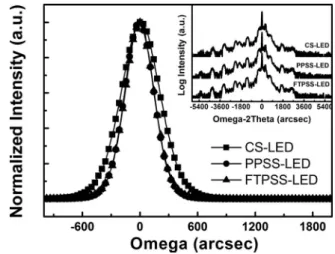
When we applied a⫺10 V reverse bias to the samples, the leakage currents of the CS sample, PPSS, and FTPSS were 557, 76.7, and 28.9 nA, respectively. We used identical epitaxy and fabrication con-ditions to prepare these samples; therefore, we attribute the rela-tively large leakage current of the CS-LED to many TDs stretching from the sapphire–GaN interface because dislocation is the main cause of leakage. For the PPSS and FTPSS, the leakage current decreased such that we consider the TDDs within these two samples to be restrained. The X-ray diffraction共XRD兲 spectra in Fig.3 con-firm the improved crystal quality.12 The full width at half-maximums in the共102兲 scans of the PPSS and FTPSS are very close共360 and 356.4 arcsec, respectively兲 and are much lower than that in the CS sample共479 arcsec兲. These values are consistent with our hypothesis of a dislocation suppression effect in the PPSS and FTPSS.
Figure4displays the electroluminescence共L-I兲 behavior of each of the samples at injection currents varying from 1 to 600 mA ap-plied directly on the chip with a metal heat-dissipating probe station. For each sample, the output intensity increased rapidly upon increas-ing the injection current from 1 to 200 mA, but increased at a much lower rate thereafter, and finally declined when the injection currents reached 460, 500, and 520 mA for the CS-, PPSS-, and FTPSS-LED,
Figure 1. SEM images of关共a兲 and 共b兲兴 PPSS and 关共c兲 and 共d兲兴 FTPSS before
performing epitaxy.
Figure 2. I-V curves of CS-, PPSS-, and FTPSS-LED recorded at room
temperature under both forward and reverse biases.
Figure 3. High resolution XRD共102兲 scans of CS-, PPSS-, and
FTPSS-LED. Inset: Corresponding共002兲 -2 scans.
H875
Journal of The Electrochemical Society, 156共11兲 H874-H876 共2009兲 H875
) unless CC License in place (see abstract).
ecsdl.org/site/terms_use
address. Redistribution subject to ECS terms of use (see
140.113.38.11
respectively. We attribute this phenomenon to the TDD within the devices. For InGaN blue LEDs, dislocation is considered to be a source of nonradiative recombination centers. When the injection current increases, the junction temperature also rises, and nonradia-tive recombination becomes stronger because of a phonon effect. As mentioned above, we suspected that the CS-LED had a higher TDD than the other two samples; therefore, its heat effect was strongest, resulting in an earlier output decay. After packing the samples with transistor-outline metal can package and inserting them into an in-tegrating sphere, we found that the CS-, PPSS-, and FTPSS-LED samples had output powers of 5.03, 5.93, and 5.97 mW, respectively, at 20 mA; i.e., relative to that of the CS-LED, the power improved to 17.9 and 18.7% when using the pyramidal and flat-top substrates, respectively. In addition to their improved crystal quality, it is be-lieved that the enhanced output was also due to the higher degrees of interfacial roughness in the patterned samples. When light emitted from an MQW reaches the interface between the patterned substrate and its epilayer, multiscattering can occur to alter the incident angle of light at the air–GaN interface, thereby increasing the probability of light escaping from the device. Furthermore, because the grain shape in the FTPSS was trapezoid-like and more irregular than that in the PPSS, the output from the FTPSS-LED was understandably higher than that from the PPSS-LED.
To further investigate strain characteristics in each sample, a power-dependent photoluminescence spectroscopy was performed at 40 K. Figure5displays the emission peak shift of different samples vs pumping power density. To emphasize peak variance, the low power excitation peak wavelengths were set to zero for all samples. As illustrated, all samples performed a blueshift trend in emission wavelength as the pumping power density went higher. The inset of Fig.3reveals that the indium contents of these samples were almost identical. The satellite peak positions are quite similar, indicating a strong structural similarity for all three samples, so it is assumed that the difference in blueshift mainly originated from the nature of sub-strates. For the CS-LED, the value of the peak shift was⫺5.5 nm while the pumping power density was raised from 1 to 80 W/cm2, which is larger than⫺3.46 and ⫺4.46 nm of PPSS- and FTPSS-LED, respectively. The internal piezoelectric field of nitrides origi-nating from the strain results in a quantum-confined Stark effect 共QCSE兲 and reduces the effective energy gap. While carriers were injected into quantum wells, the charge screening effect occurred and restrained QCSE, which resulted in an emission peak blueshift. Because the CS-LED had the largest power-dependent blueshift among all samples, it was inferred that its QCSE was also the stron-gest. Wuu et al. proposed that air voids can exist upon tilt facets of patterns as a result of growth rate differences of the nitride between flat and inclined facets;8Park et al. also observed such voids in a
semisphere PSS sample.13In both studies, the PSS was considered able to alter the strain in LEDs. For the convex patterned samples reported in this work, it was suspected that such kind of strain effect could also occur within the devices. In consideration of surface mor-phology, the epilayer of the CS-LED is almost fully contacted to the sapphire substrate, which leaves a strong residual strain within quan-tum wells. Similar to the CS-LED, because the FTPSS-LED has a flat surface on top, its contact area is also larger than the PPSS-LED; thus the emission peak shifted slightly faster as the pumping power went up.
We prepared convex patterned sapphire substrates featuring flat-top and pyramid grains using single and two-step wet etching meth-ods, respectively. The output powers of LEDs incorporating the PPSS and FTPSS were up to 18.7 and 17.9% high, relative to that of the corresponding LED featuring a CS. Meanwhile, the leakage cur-rents also decreased remarkably as a result of lower TDDs. A stron-ger QCSE was found in the CS-LED and, compared to the PPSS-and FTPSS-LED, indicates a higher residual strain. This shows that a convex patterned sapphire substrate could not only enhance output power of LEDs but also lower residual strain within quantum wells.
Chang Gung University assisted in meeting the publication costs of this article.
References
1. S. Nakamura, M. Senoh, N. Iwasa, and S. Nagahama, Jpn. J. Appl. Phys., Part 2, 34, L797共1995兲.
2. S. Nakamura and G. Fosel, The Blue Laser Diode, Springer-Verlag, Berlin共1997兲. 3. E. F. Schubert, Light Emitting Diodes, 1st ed., Cambridge University Press,
Cam-bridge, MA共2003兲.
4. T. S. Zheleva, O. H. Nam, M. D. Bremser, and R. F. Davis, Appl. Phys. Lett., 71, 2472共1997兲.
5. A. Sakai, H. Sunakawa, and A. Usui, Appl. Phys. Lett., 71, 2259共1997兲. 6. C. H. Chiu, H. H. Yen, C. L. Chao, Z. Y. Li, P. C. Yu, H. C. Kuo, T. C. Lu, S. C.
Wang, K. M. Lau, and S. J. Chang, Appl. Phys. Lett., 93, 081108共2008兲. 7. F. Dwikusuma, D. Saulys, and T. F. Kuech, J. Electrochem. Soc., 149, G603
共2002兲.
8. D. S. Wuu, W. K. Wang, K. S. Wen, S. C. Huang, S. H. Lin, R. H. Horng, Y. S. Yu, and M. H. Pan, J. Electrochem. Soc., 153, G765共2006兲.
9. S. J. Kim, Jpn. J. Appl. Phys., Part 1, 44, 2921共2005兲.
10. J. Wang, L. W. Guo, H. Q. Jia, Y. Wang, Z. G. Xing, W. Li, H. Chen, and J. M. Zhou, J. Electrochem. Soc., 153, C182共2006兲.
11. T. V. Cuong, H. S. Cheong, H. G. Kim, H. Y. Kim, C. H. Hong, E. K. Suh, H. K. Cho, and B. H. Kong, Appl. Phys. Lett., 90, 131107共2007兲.
12. B. Heying, X. H. Wu, S. Keller, Y. Li, D. Kapolnek, B. P. Keller, S. P. DenBaars, and J. S. Speck, Appl. Phys. Lett., 68, 643共1996兲.
13. E. H. Park, J. Jang, S. Gupta, I. Ferguson, C. H. Kim, S. K. Jeon, and J. S. Park, Appl. Phys. Lett., 93, 191103共2008兲.
Figure 4. L-I profiles of CS-, PPSS-, and FTPSS-LED.
Figure 5. Emission peak shifts vs pumping power density for CS-, PPSS-,
and FTPSS-LED. Dashed, dotted, and dashed-dotted lines correspond to their peak-shifting ratio.
H876 Journal of The Electrochemical Society, 156共11兲 H874-H876 共2009兲
H876
) unless CC License in place (see abstract).
ecsdl.org/site/terms_use
address. Redistribution subject to ECS terms of use (see
140.113.38.11