j o u r n a l o f m a t e r i a l s p r o c e s s i n g t e c h n o l o g y 2 0 6 ( 2 0 0 8 ) 425–430
j o u r n a l h o m e p a g e : w w w . e l s e v i e r . c o m / l o c a t e / j m a t p r o t e c
Fabrication and characterization of eutectic gold–silicon
(Au–Si) nanowires
Jin-Shyong Lin
a, Chien-Chon Chen
b, Eric Wei-Guang Diau
b,∗, Tzeng-Feng Liu
aaDepartment of Material Science and Engineering, National Chiao Tung University, Hsinchu 30010, Taiwan
bDepartment of Applied Chemistry and Institute of Molecular Science, National Chiao Tung University, Hsinchu 30010, Taiwan
a r t i c l e
i n f o
Article history:
Received 13 April 2007 Received in revised form 5 November 2007 Accepted 15 December 2007 Keywords: AAO Au–Si alloy Die-casting Eutectic nanowire Vacuum smelting
a b s t r a c t
Hypoeutectic, eutectic and hypereutectic gold–silicon (Au–Si) alloys were synthesized using vacuum smelting. When Au and Si were smelted in a vacuum chamber near 1100◦C, Si(g), Si2(g), Si3(g), SiO2(g), Au(g), SiO2(s)and Au2O3(s)were formed rapidly; the quantities of Au and Si lost were estimated from thermodynamic formulas. The nano- and microstructures of the Au–Si eutectic compound were characterized with a SEM and a TEM, which showed a discontinuous phase of Si dispersed and mounted within a matrix phase of Au. Cracks that formed about the Au–Si interface made the Au–Si eutectic brittle. From an Au–Si alloy of superior quality as a bulk material, eutectic nanowires of average diameter 60 nm were fabricated after the alloy was melted and injected into an anodic aluminum-oxide (AAO) template.
© 2008 Elsevier B.V. All rights reserved.
1.
Introduction
Gold is a conductive noble metal, and silicon is a base mate-rial for the semiconductor industry. Gold is commonly used in semiconductor products. For example, an Au–Si eutectic alloy is used for microchip packing and interconnection in micro-electro-mechanical systems (MEMS). As an Au–Si eutectic has a useful field-emission property, it serves for panels or dis-plays; for example, a 70-nm Au–Si eutectic tip has an initiating field only 10 Vm−1 (Wan et al., 2004). Furthermore, when
an Au–Si eutectic is set on a 10-m tip, a large field current 300A is obtainable on the tip (Zhirnov et al., 1996). Although such an Au–Si alloy has excellent electronic characteristics, the mechanical properties of such an Au–Si alloy are gener-ally detrimental to product quality. According toKomatsu and
Kiritani (2003), an Au–Si eutectic becomes brittle upon
subjec-tion to the cold-rolling process. Gold is a ductile material, but
∗Corresponding author. Fax: +886 3 572 3764.
E-mail addresses:[email protected](C.-C. Chen),[email protected](E.W.-G. Diau).
a small proportion of brittle silicon in gold makes the alloy become brittle.
According to the Au–Si binary phase diagram (Massalski, 1987) shown inFig. 1, the melting points of Au and Si are 1064◦C and 1414◦C, respectively, whereas the eutectic point has a melting point only 363◦C. No compound formation of any composition occurs in an Au–Si alloy, but three alloy phases – hypoeutectic, eutectic and hypereutectic – appear in the Au–Si diagram. When the temperature is greater than that of the liquid line, mixed Au and Si in a liquid phase appear; hypoeutectic and hypereutectic phases appear when the temperature decreases along hypoeutectic and hypereu-tectic lines.
The fabrication of nanowires by non-lithographic meth-ods such as ion deposition has been reported (Komatsu and Kiritani, 2003; Massalski, 1987; Wang et al., 2001; Zhang et al.,
2000; Nielsch et al., 2001). Problems are associated with ion
0924-0136/$ – see front matter © 2008 Elsevier B.V. All rights reserved.
426
j o u r n a l o f m a t e r i a l s p r o c e s s i n g t e c h n o l o g y 2 0 6 ( 2 0 0 8 ) 425–430Fig. 1 – Au–Si phase diagram: hypoeutectic composition of point a (2.3 mass% Si–Au), eutectic composition of point b (2.8 mass% Si–Au), and hypereutectic composition of point c (4.0 mass% Si–Au).
Fig. 2 – Schematic diagram of Au–Si alloys made with vacuum smelting: (a) ratio (mass%) of Au and Si in the vacuum tube and (b) after heating, Au–Si alloys formed in the tube.
Fig. 3 – OM images of Au–Si alloys: (a) Si–Au of hypoeutectic (2.3 mass%), (b) Si–Au of eutectic (2.8 mass%), and (c) Si–Au of hypereutectic (4.0 mass%).
Table 1 – Thermodynamic equilibrium reactions in the Au–Si–O system
Reaction Equations log K
Si(s)→ Si(g) logPSi(g)= log K 7.694− (23447.16/T)
2Si(s)→ Si2(g) logPSi2(g)= log K 3.505− (26942.52/T)
3Si(s)→ Si3(g) logPSi3(g)= log K 10.465− (32920.81/T)
Si(s)+ O2(g)→ SiO2(g) logPSiO2(g)= log K + log PO2(g) 0.0672 + (16043.28/T)
Si(s)+ O2(g)→ SiO2(s) logPO2(g)= −log K 9.252 + (47410.44/T)
Au(s)→ Au(g) logPAu(g)= log K 6.6484− (19083.24/T)
j o u r n a l o f m a t e r i a l s p r o c e s s i n g t e c h n o l o g y 2 0 6 ( 2 0 0 8 ) 425–430
427
Fig. 4 – DSC thermographs of Au–Si alloys: the melting points of (a) Si–Au (2.3 mass%) at 480◦C, (b) Si–Au (2.8 mass%) at 363◦C, and (c) Si–Au (4.0 mass%) at 520◦C.
deposition, such as a large cost of instruments and a small yield, and the quality of nanowires is jeopardized by the pres-ence of a catalyst required for the ion deposition. In contrast, metal casting is a method well established in metallurgy. The experience gained from this traditional casting combined with emerging nanotechnological methods are prospectively useful in minimizing the cost of nanomaterial fabrication, improving the efficiency of fabrication, and decreasing the complication of the fabrication. For these reasons we fabricated hypoeu-tectic, eutectic and hypereutectic Au–Si alloys using vacuum smelting; we subsequently formed Au–Si eutectic nanowires by vacuum die-casting using an anodic aluminum-oxide (AAO) thin film as a template.
2.
Experiments
Au–Si alloys with three compositions—hypoeutectic (2.3 mass% Si–Au, sample a), eutectic (2.8 mass% Si–Au,
sam-Fig. 5 – Vapor pressures of Au and Si as a function of temperature.
Fig. 6 – Equilibrium partial pressures of oxygen in (a) Au/Au2O3, (b) Si/SiO2(s), and (c) Si/SiO2(g).
ple b), and hypereutectic (4.0 mass% Si–Au, sample c), were fabricated using vacuum smelting. Highly pure (99.99%) gold foil and single-crystal silicon wafers were used for the Au–Si alloys. Samples a–c were placed in quartz tubes that were then evacuated (P∼ 3 × 10⁻⁶Torr) with a turbo molecular pump,
purged with argon, and sealed in an oxyacetylene flame. The sealed tubes were heated at 1100◦C for 1 h, with occasional agitation to achieve a homogeneous melt. A schematic dia-gram is presented inFig. 2. The melt was then cooled in air to form Au–Si bulk alloys. The metallurgical microstructure and composition of the alloys were examined with an optical microscope (Olympus BX51), a scanning electron microscope
428
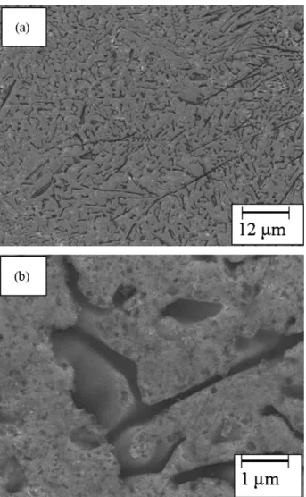
j o u r n a l o f m a t e r i a l s p r o c e s s i n g t e c h n o l o g y 2 0 6 ( 2 0 0 8 ) 425–430Fig. 7 – SEM images of (a) Au–Si eutectic, (b) zoomed image, and (c) EDS diagram.
(JEOL 6500F FESEM), X-ray diffraction (Bruker D8), and a differ-ential scanning calorimeter (PerkinElmer Pyris 1). The thermo-dynamic reaction between Au, Si and O2at high temperature
was evaluated using thermodynamic data (Chase et al., 1985). An AAO template (thickness 57m) and ordering arrays (pore size 60 nm) were made in oxalic-acid electrolyte (3 mass%); a detailed procedure for AAO fabrication is found elsewhere (Chen et al., 2005; Lin et al., 2006a,b). The Au–Si eutectic nanowires were fabricated using vacuum die-casting
(Chen et al., 2006). The morphology of the nanowires was
characterized with a SEM, a TEM and an energy dispersive spectrometer (EDX).
3.
Results and discussion
Fig. 3 shows OM images of samples a (hypoeutectic), b
(eutectic), and c (hypereutectic) after vacuum smelting. The continuous matrix phase is Au, and the discontinuous gray phase is Si. According to the figures, the hypoeutectic has an Au-rich phase (a); the eutectic has homogenous Au and Si mixed phases (b), and the hypereutectic has a Si-rich phase (c). InFig. 4, DSC curves show the melting points of
sam-Fig. 8 – SEM images of AAO: (a) top view and (b) side view.
ples a, b and c – 480, 363 and 520◦C, respectively – matching those shown in Fig. 1. According to the results shown in
Figs. 3 and 4, we demonstrated that stoichiometric alloys are
obtained according to our experimental conditions.
At high temperatures Au and Si readily form oxides and vaporize: for example, the species SiO2(s), Si(g), Si2(g), Si3(g)and
SiO2(g)form in the Si–O system, and Au(g)and Au2O3(s)form in
the Au–O system. The formation of these species causes a loss of composition during alloy smelting; the quantity lost was estimated through a thermodynamic calculation. The reac-tions of Au, Si, and O2are presented in Table 1, in which P
denotes partial pressure (atm), T temperature (K), and K equi-librium quotient (Chase et al., 1985).Fig. 5shows the partial pressures of Au and Si gases as a function of temperature: the partial pressure increases with temperature in an order Au(g)> Si(g)> Si2(g)> Si3(g).Fig. 6shows the threshold pressure
of O2of Au and Si for oxidation to Au2O3(s), SiO2(g)and SiO2(s).
The curves show an increasing order Au2O3(s)> SiO2(g)> SiO2(s),
indicating that the formation of SiO2(s)has a smaller
thresh-old of O2 pressure than formation of Au2O3(s) and SiO2(g).
Hence Au(g)and SiO2(s)are readily lost during Au–Si smelting.
Although the pressure of O2in the vacuum chamber was small
during vacuum smelting, the loss of Au(g)increased with
j o u r n a l o f m a t e r i a l s p r o c e s s i n g t e c h n o l o g y 2 0 6 ( 2 0 0 8 ) 425–430
429
Fig. 9 – SEM images of Au–Si eutectic nanowire in the AAO template: (a) top view, (b) side view, and (c) nanowires removed from the AAO.
Au lost during vacuum smelting is greater than that of Si. In our experiment, the extra Au (0.2 mass%) was added over the eutectic point for Au–Si eutectic formation.
A compound with a ductile matrix and a brittle precip-itation structure is typically ductile in bulk. For example, a eutectoid structure of pearlite forms with a ductile Fe matrix and a discontinuous brittle cementite (Fe3C) precipitation
phase (Callister, 1994); a eutectic structure of Sn–Bi alloy forms with a ductile Sn matrix and a discontinuous brittle Bi precipi-tation phase. The Pb–Bi eutectic is likewise ductile in bulk, but an Au–Si eutectic alloy is a brittle material.Fig. 7shows SEM
Fig. 10 – TEM images of (a) Au–Si eutectic nanowire and (b) zoomed image of black particle (Si).
images of the Au–Si eutectic microstructure. In the image of
Fig. 7(a) at small magnification, a discontinuous phase of Si
disperses into the matrix phase of Au. In the image presented in (b) at large magnification, Si is mounted inside Au, and cracks have formed about the Au–Si interface; this cracking makes the Au–Si eutectic brittle. In Au–Si phase diagram, Au and Si cannot form alloy in the Au–Si melt mixture. When the melt mixture was solidified, the solid phases of Au and Si were formed separately. Because the thermal condense coefficients of Au and Si are different (Au: 14.2× 10⁻⁶K−1, Si: 2.6× 10⁻⁶K−1)
(Dean, 1992), the Au–Si mixture cracks easily, as shown in (b).
Fig. 8shows SEM images of AAO with ordered
nanochan-nels at the packing density 4× 1011cm−2. The pores have
diameter 60 nm and length 57m. An AAO template of satis-factory quality is required for fabrication of Au–Si nanowires.
Fig. 9(a) (top view) and (b) (side view) show SEM images of Au–Si
eutectic nanowires produced on vacuum die-casting with an AAO template; (c) shows Au–Si nanowires after the template was dissolved in phosphoric acid (20 vol.%). The diameter and length of the nanowires depend on the AAO size; in this case, the Au–Si eutectic nanowires have diameter∼60 nm and length∼57 m. To investigate the detailed morphology of indi-vidual nanowires that were deposited on a Cu grid after the AAO template was thoroughly dissolved, we employed a TEM: two TEM images of a randomly selected nanowire appear in
430
j o u r n a l o f m a t e r i a l s p r o c e s s i n g t e c h n o l o g y 2 0 6 ( 2 0 0 8 ) 425–4304.
Conclusion
Using vacuum smelting method Au–Si hypoeutectic, eutec-tic, and hypereutectic alloys were fabricated. Because more Au than Si is lost during this smelting, the extra Au was added to the alloy to achieve an Au–Si eutectic alloy with the correct stoichiometry. The melting points and microstruc-tures of alloys were measured with a differential scanning calorimeter and an optical microscope; these results cor-related satisfactorily with the Au–Si phase diagram. Au–Si eutectic nanowires of diameter∼60 nm have been successfully made with die-casting and AAO as a template. SEM and TEM images show the morphology of the nanostructure of Au–Si eutectic nanowires with Si nanoparticles dispersed in the Au matrix.
Acknowledgements
National Science Council of Republic of China (contract 95-2113-M-009-027) and the MOE-ATU program provided financial support.
r e f e r e n c e s
Callister Jr, W.D., 1994. Materials Science and Engineering–An Introduction, 3rd ed. Wiley, New York, USA, p. 269. Chase Jr., M.W., Davies, C.A., Downey Jr., J.R., Frurip, D.J.,
McDonald, R.A., Syverud, A.N., 1985. JANAF thermochemical tables. J. Phys. Chem. Ref. Data, USA 1650 (1673–1678), 1795–1803.
Chen, C.C., Chen, J.H., Chao, C.G., 2005. Post-treatment method of producing ordered array of anodic aluminum oxide using general purity commercial (99.7%) aluminum. Jpn. J. Appl. Phys. 44, 1529.
Chen, C.C., Bisrat, Y., Luo, Z.P., Schaak, R.E., Chao, C.-G., Lagoudas, D.C., 2006. Fabrication of single-crystal tin nanowires by hydraulic pressure injection. Nanotechnology 17, 367. Dean, J.A., 1992. Lange’s Handbook of Chemistry, 14th ed.
McGraw-Hill, New York.
Komatsu, M., Kiritani, M., 2003. Amorphization of eutectic alloys by shock compression. Mater. Sci. Eng. A 350, 150.
Lin, J.S., Chen, Y.C., Chen, C.-C., Diau, E.W.-G., Liu, T.-F., 2006a. Aggregation of zinc protoporphyrin in anodized aluminum oxide (AAO) nanoporous environments. J. Chin. Chem. Soc. 53, 201.
Lin, J.S., Chen, Y.C., Chen, C.-C., Luo, L.-Y., Diau, E.W.-G., Liu, T.-F., 2006b. Fluorescence dynamics of zinc protoporphyrin in solution and inside anodized aluminum oxide (AAO) nano-channel arrays. J. Chin. Chem. Soc. 53, 1405.
Massalski, T.B., 1987. Binary alloy phase diagrams. Am. Soc. Met., USA, 313.
Nielsch, K., Wehrspohn, R.B., Barthel, J., Kirschner, J., Gosele, U., Fischer, S.F., Kronmuller, H., 2001. Hexagonally ordered 100-nm period nickel nanowire arrays. Appl. Phys. Lett. 79, 1360.
Wan, Q., Wang, T.H., Lin, C.L., 2004. Self-assembled Au–Si alloy nanocones: synthesis and electron field emission
characteristics. Appl. Surf. Sci. 221, 38.
Wang, B., Yin, S., Wang, G., Buldum, A., Zhao, J., 2001. Novel structures and properties of gold nanowires. Phys. Rev. Lett. 86, 2046.
Zhang, Y.F., Tang, Y.H., Wang, N., Lee, C.S., Bello, I., Lee, T., 2000. Germanium nanowires sheathed with an oxide layer. Phys. Rev. B 61, 4518–4521.
Zhirnov, V.V., Bormatova, L., Givargizov, E.I., 1996. Field emission properties of Au–Si eutectic. Appl. Surf. Sci. 94/95, 144.