國 立 交 通 大 學
電子工程學系 電子研究所 碩士班
碩 士 論 文
在晶片與封裝共同設計時對於核心區塊
與輸入輸出緩衝器擺置的方法
A Block and I/O Buffer Placement Methodology for
Chip-Package Codesign
研 究 生:賴明芳(Ming-Fang Lai)
指導教授: 陳宏明 教授(Prof. Hung-Ming Chen)
在晶片與封裝共同設計時對於核心區塊
與輸入輸出緩衝器擺置的方法
A Block and I/O Buffer Placement Methodology for
Chip-Package Codesign
研 究 生:賴明芳 Student:Ming-Fang Lai
指導教授:陳宏明 教授 Advisor:Professor Hung-Ming Chen
國 立 交 通 大 學
電 子 工 程 學 系 電 子 研 究 所 碩 士 班
碩 士 論 文
A Thesis
Submitted to Department of Electrical Engineering & Institute of Electronics
College of Electrical Engineering and Computer Science
National Chiao Tung University
in Partial Fulfillment of the Requirements
for the Degree of
Master of Science
in
Electronics Engineering
October 2006
Hsinchu, Taiwan, Republic of China
在晶片與封裝共同設計時對於核心區塊
與輸入輸出緩衝器擺置的方法
學生:賴明芳 指導教授:陳宏明 教授
國立交通大學 電子工程學系 電子研究所碩士班
摘 要
隨著矽製程的發展,我們能夠在單一個晶片中放置越來越多
的電路。這代表了越進步的設計將需要越多的輸入輸出訊
號。覆晶封裝方式是 IBM 在 1960 年代所發展出來的,它比
典型的周邊打線接合方式在輸出入訊號上能提供更多的個
數,覆晶設計其中一個最重要的特性就是輸出入緩衝器可以
像核心電路一樣放在晶片內的任何一個地方。在這邊論文
裡,我們發展了一個在覆晶設計時,核心區塊與輸出入緩衝
器擺置的演算法並且同時考量接線長度、訊號歪斜與電源完
整性.
A Block and I/O Buffer Placement Methodology for
Chip-Package Codesign
Student: Ming-Fang Lai Advisor: Prof. Hung-Ming Chen
Department of Electronics Engineering
Institute of Electronics
National Chiao Tung University
ABSTRACT
As silicon technology scales, we can integrate more and more circuits
on a single chip,which means more I/Os are needed in modern designs.
The flip-chip packaging was developed by IBM in 1960's. It is better than
the typical peripheral wire-bond design in the increase in I/O count. One
of the most important characteristics of flip-chip designs is that the input
and output buffers could be placed anywhere inside a chip, like core cells.
In this thesis, we develop an block and I/O buffer placement algorithm in
wire length and signal skew optimization and power integrity concerning
for flip-chip design.
誌 謝
能完成這篇論文,我最感謝的是我的指導教授陳宏明教授。兩年
來為我們付出無比的耐心和關懷,不僅僅是課業上,還有生活上待人
處事的道理,都使我們受益良多。陳教授是一位難得的良師兼益友,
在學識上和生活上都給我們完善的照顧和關懷,真的很感謝也很高興
能有這個機會當陳教授的學生。
同時也感謝口試委員麥偉基教授、邱碧秀教授的指導和啟發,讓
我在口試時能夠更進ㄧ步的思考,並不僅僅是寫一篇論文而已。
我還要感謝我的朋友和同學,他們的幫忙,讓我順利地完成論文。
最後,我很感謝父母和女友。他們的支持,是我努力做研究的動
力。
A Block and I/O Buffer Placement Methodology
for Chip-Package Codesign
Student : Ming-Fang Lai
Advisor: Prof. Hung-Ming Chen
Department of Electronics Engineering
Institute of Electronics
Contents
1 Introduction 1
1.1 Our Contributions . . . 3
1.2 Organization of this Thesis . . . 4
2 Preliminaries 5 2.1 Flip-Chip Design Constraints . . . 5
2.1.1 Skew and Path Delay Constraints . . . 5
2.1.2 Differential Pair Constraint . . . 7
2.1.3 Power Integrity Constraint . . . 7
2.2 Previous Works . . . 8
2.2.1 Simultaneous Block and I/O Buffer Floorplanning for Flip-Chip Design . . . 8
2.2.2 Constraint Driven I/O Planning and Placement for Chip-package Co-design . . . 8
2.2.3 I/O Buffer Placement Methodology for ASICs . . . 9
3.1 Block Placement . . . 11 3.2 Buffer Placement . . . 15
4 Experimental Results 17
5 Conclusion and Future Work 21
List of Figures
1.1 Example layout of the flip-chip[2]. . . 2 1.2 Cross section of RDL[2]. . . 2 2.1 Example of path delay calculation, the orders from left to right are
bump, I/O buffer and block[2]. . . 6 3.1 After putting all charge counters, every grid has a number of
coun-ters. Small triangles mean charge counters, big rectangles mean core blocks, and three numbers next to rectangle are three candidates. Small circles are signal bumps that connect to the ports on each blocks through I/O buffers. . . 12 3.2 After grid assignment, each block sit at the left-bottom of the grid. . 13 3.3 Case3 Blocks placement before rectification step(we only assign each
block roughly in the left-bottom of a grid or next to the boundary. . 14 3.4 Case3 Blocks placement after rectification step(without any overlap). 14 3.5 If a grid does not have enough supporting power, buffer will find
another grid to place.(the two big rectangle means block, the small one means buffer) . . . 15
4.1 Power integrity exhibition before and after concern of case5(fc5). The upper figure has a hot spot that drains more power then the other grids . . . 18 4.2 The blocks and I/O buffers placement result of fc3. . . 20
List of Tables
4.1 Statistics of the test circuits[2] . . . 17 4.2 Experimental results of our placement method and [1] where the CPU
time of [1] was measured on a 1.2GHz workstation with 8GB memory. This table shows the effectiveness of our approach . . . 19
Chapter 1
Introduction
As silicon technology scales, we can integrate more and more circuits on a single chip,which means more I/Os are needed in modern designs. The flip-chip packaging was developed by IBM in 1960’s. It is better than the typical peripheral wire-bond design in the increase in I/O count. One of the most important characteristics of flip-chip designs is that the input and output buffers could be placed anywhere inside a chip, like core cells. In this thesis, we develop an block and I/O buffer placement algorithm in wire length and signal skew optimization and power integrity concerning for flip-chip design.
Flip-chip packaging gives the highest chip density to support the pad-limited ASIC design. One of the best advantages of flip-chip packaging is that signal noise can be reduced because the inductance of the wire is much less than the traditional wire bonding method. And power distribution is also much more balance because the power ground networks can distribute power more easily by the middle bump on the chip. At the same time, flip-chip packaging offers a different way to place I/O pad (I/O buffer), we can put it into the chip just next to the core cells and again shorter the wire length. Figure 1.1 show the example layout of the flip-chip. We use the top metal or an extra metal layer, called Re-Distributed Layer (RDL), to connect input or output buffers to bump balls. Figure 1.2 shows the cross section
Figure 1.1: Example layout of the flip-chip[2].
of RDL. Bump balls are placed on RDL and use RDL to connect to I/O buffers. In some memory-related designs, such as memory controllers, there are a large number of paths being used as data bus. For these designs, we must control the timing of I/O signals. So we have to make sure input signals arrive at the core simultaneously. Similarly, we also have to make sure output signals arrive at bump balls simultaneously. The placement problem for the classical wire-bond ICs has been studied very extensively [14,15,16,17]. Nevertheless, most of these previous works target on standard cell designs, for which cells are of the same height and are placed in rows. Peng et al.[1] studied the problem of I/O buffer placement in flip-chip design and proposed a placement methodology based on hierarchical top-down method using the B* tree representation. Jinjun Xiong et al.[5] took many real design constraints into consider, such as timing closure, signal integrity (SI) and power integrity for chip-package co-design. Kozhaya et al. [6] studied the problem of I/O buffer placement in flip-chip design and proposed a placement methodology that avoids severe voltage drop. Since flip-chip allows I/O buffer to be placed any where in the chip, we need to focus on the change to better design and methodology have been presented in the literature[8,9,10,11,12], dealing with I/O placement and electrical checking using flip-chip technology. In [13]they utilized flip-chip design to minimize interconnect length which is the major concern in I/O placement. Recently, [4] further consider the building cost of buffer block. In this thesis, we develop a heuristic way to place blocks and I/O buffers. At the same time, we also considere timing closure and power integrity in this problem.
1.1
Our Contributions
In this thesis, we develop a block and I/O buffer placement algorithm in wire length, signal skew optimization and power integrity for flip-chip design. Moreover, we add
average skew of differential pairs (in Table 4.2) and power integrity improvement of whole chip (in Figure 4.1).
1.2
Organization of this Thesis
The remainder of this thesis is organized as follow. Chapter 2 describes the cost function modeling, previous works and problem formulation. Chapter 3 describes our methodology flow, divided in two parts, block placement and buffer placement. Chapter 4 show the experimental results. Chapter 5 presents the conclusion and future work.
Chapter 2
Preliminaries
In this problem, we assume the chip area is pre-defined. All bump balls are placed at pre-defined locations, and their signals are determined. All core cells have been partitioned or grouped into blocks, and there are block ports to connect to input or output buffers. All I/O signals are connected between bump balls and block ports through I/O buffers. For some signals such as differential pair ,their skew will be reduced as soon as possible. Not only skew, but also power integrity problem and differential pair constraint should be notice.
2.1
Flip-Chip Design Constraints
2.1.1
Skew and Path Delay Constraints
For most practical designs, as mentioned earlier, there are a large number of in-put/output pins being used for data buses. Therefore, it is also desired to make sure that all input signals from bump balls via input buffers to blocks arrive si-multaneously and output signals from blocks via output buffers to bump balls also arrive simultaneously. To achieve the goal, we define the objective function Γ as follows:[1]
Φ1 = µ max 1≤j≤n1d i j − min1≤j≤n1dij ¶2 + µ max 1≤j≤n2d o j − min1≤j≤n2doj ¶2 (2.2) Φ2 = n1 X j=1 dij + n2 X j=1 doj (2.3)
We notice that α is the weighting factor about skew, β is the weighting factor about wire length. Φ1 gives the sum of path delays, and Φ2 gives the sum of the
squares of the maximum input and output signal skews. n1 and n2 are the numbers of input and output signals, respectively. di
j and doj are the path delays of the jth
input signal and the jth output signal, respectively. The path delay of an input
signal is the delay of a path from a bump ball via an input buffer to a block port of a block; the path delay of an output signal is the delay of a path from a block port of a block via an output buffer to a bump ball.
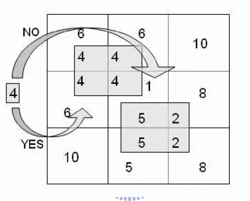
Figure 2.1: Example of path delay calculation, the orders from left to right are bump, I/O buffer and block[2].
input buffer, I1, is (40, 50) and its input and output port coordinates are (0, 10) and (0, 30), respectively. The coordinate of block, BL1, is (200, 300) and its block port is (0, 30). The path delay from BA1 via I1 to the block port of BL1 is the summation of the delay from BA1 to the input port of I1 and the delay from the output port of I1 to the block port of BL1. The delay from BA1 to the input port of I1 is equal to
|10 − (40 + 0)| + |10 − (50 + 10)| = 80. The delay from the output port of I1 to the
block port of BL1 is equal to |(50 + 30) − (300 + 30)| + |(40 + 0) − (200 + 0)| = 410. So that path delay from the bump ball to the block is equal to 490.
2.1.2
Differential Pair Constraint
We additionally add a number of differential pairs (3 to 20 pairs in five cases). Dif-ferential pair signals often referenced by particular circuits, their allowance of skew is usually lower than normal circuits. In modern designs, signal skew influences chip performance greatly. A common practice to lower the skew is to place differential pairs close to each other so that the corresponding package routes will have similar route length[5]. We shorter the skew of differential pairs by making the path delay of two signals approaches to each other preferably. We will also show the results about the average skew of the differential pairs in Chapter 4.
2.1.3
Power Integrity Constraint
Flip-chip technology allows high-performance ICs and microprocessors to be built with many more power and I/O connections than in the past. In order to completely take advantage of this technology, we need to focus on the placement of highly power hungry buffers, namely I/O buffers[4]. Then we consider the power integrity in whole chip. If a region accumulates too many buffers(or blocks), the power supporting ability should be noticed. We try to distribute the power draining to
that had supply to blocks and buffers. Area Grid means total area of each grid.
P ower Supply Rate determines the power supply ability by unit area of grid.
Supplied P ower < Area Grid ∗ P ower Supply Rate (2.4)
2.2
Previous Works
2.2.1
Simultaneous Block and I/O Buffer Floorplanning for
Flip-Chip Design
Peng et al.[1] studied the problem of I/O buffer placement in flip-chip design and proposed a placement methodology based on hierarchical top-down method using the B* tree representation. They first cluster a block and its corresponding buffers to reduce the problem size. Then, go into iterations of the alternating and inter-acting global optimization step and the partitioning step. The global optimization step places blocks based on simulated annealing using the B*-tree representation to minimize a given cost function. The partitioning step dissects the chip into two subregions, and the blocks are divided into two groups and are placed in respective subregions. The two steps repeat until each subregion contains at most a given number of blocks, defined by the ratio of the total block area to the chip area. At last, they refine the floorplan by perturbing blocks inside a subregion as well as in different subregions.
2.2.2
Constraint Driven I/O Planning and Placement for
Chip-package Co-design
Xiong et al.[5] took many real design constraints into consideration, such as timing constraints, signal integrity(SI) constraints, power integrity constraints[7], I/O
stan-I/O placement problem (CIOP) has been formulated and solved effectively via a multi-step algorithms. The major contributions of this paper include: (1) a formal definition of a set of design constraints suitable for chip-package co-design; (2) a new formulation of constraint driven I/O placement problem (CIOP); and (3) an effective multi-step algorithm to solve CIOP for chip-package co-design. It is the first auto-matic I/O planning and placement algorithm available in industry for chip-package co-design.
2.2.3
I/O Buffer Placement Methodology for ASICs
Kozhaya et al.[6] studied the problem of I/O buffer placement in flip-chip design and proposed a placement methodology that avoids severe voltage drop. One important technique to avoid severe voltage drop is to spread power hungry buffers and mod-ules so that they are spread all over the chip as opposed to keeping them densely populated in certain areas thus creating hot spots. Making the grid more robust by using a denser grid structure or wider metal lines and placing on-chip decoupling capacitors that significantly suppress high frequency components of the voltage drop are also can avoid hot spots. In this paper, by proper modeling of the power grids, source, and drains, the problem is defined mathematically and formulated as an ILP problem. To avoid the complexity of an ILP solution, a greedy heuristic is proposed and tested on two real ASIC designs with good results.
2.3
Problem Formulation
Performance of a digital system is measured by its cycle time. Shorter cycle time means higher performance. With considering the performance of a design at the layout level, signal propagation time and signal skew are two main factors. signal propagation time is defined as the path delay of the signal. Signal skew is defined
better the performance of the design, it is desirable to minimize the longest path delay and the signal skew. Besides, power integrity problem is also an important issue, a chip with bad power distribution will not have good performance.
Chapter 3
Proposed Methodology
Our methodology was divided into two parts, one is block placement step, another is buffer placement step. In block placement step, we place the block with more signals first,and minimize the total wire length and minimize the skew at the same time. We use one kind of grid assignment methodology to chose grid to place block. Blocks can rotate, but they will not overlap after the placement step. In buffer placement step, we put the I/O buffers in horizontal and vertical way. For skew purpose, I/O buffers path delay should not be too long or too short, especially the differential pairs. And for power integrity purpose, number of I/O buffer placed in each grid should have a limit (SPG signal power ratio).[5]
3.1
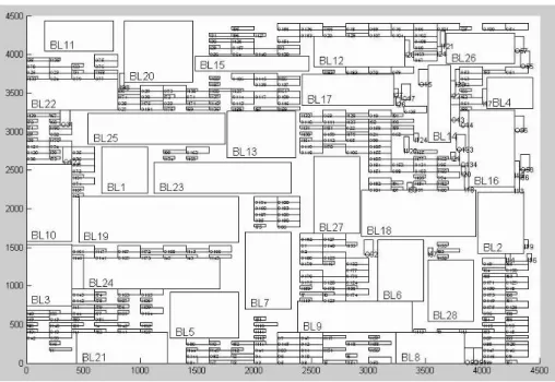
Block Placement
At first, we cut the whole chip in to n*n grids, n depends on the block numbers. For example, we chose n=4 when we have 12 blocks(4*4=16>=12), we chose n=5 when we have 23 blocks(5*5=25>=23). Then we calculate the cost of each block in each grid, and chose the best three grids and record the best three grids suitable for each block. So that each block has three candidates. If a grid is the best place for someone block, we add two charge counters on this grid. If a grid is the second place for someone block, we add one charge counter on this grid.If a grid is the third
Figure 3.1: After putting all charge counters, every grid has a number of counters. Small triangles mean charge counters, big rectangles mean core blocks, and three numbers next to rectangle are three candidates. Small circles are signal bumps that connect to the ports on each blocks through I/O buffers.
place for someone block, we add one charge counter on this grid. Fig 3.1 show the diagram of case1(fc1) after putting all charge counters. Small triangles mean charge counters, big rectangles mean core blocks, and three numbers next to rectangle are three candidates. Small circles are signal bumps that connect to the ports on each blocks through I/O buffers.
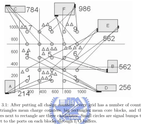
So we know that which grid is the popular grid(with most charge counters), then we put the fittest block(fittest mean that this grid is one of the three candidates of this block and this block has most number of signals at the same time) in to the grid, and remove all the charge counter put by this block. Repeat this step until all
Figure 3.2: After grid assignment, each block sit at the left-bottom of the grid.
we get the result of grid assignment block by block, as shown in Figure 3.2 .
After putting every block into grids, we start rotation step. We can rotate four direction for each block for less wire length. After this step, all the blocks chose the best rotation of the fewest cost of wire length and skew.
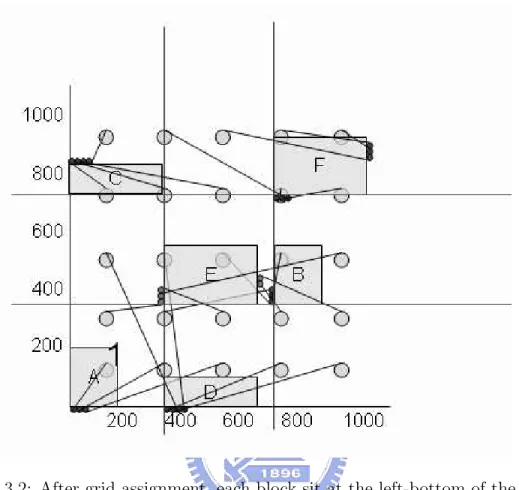
After rotation step, we start movement step. Before this step we move each block roughly in the left-bottom of a grid or next to the boundary. It may reduce overlap section slightly. Then we got blocks’s position shown in Figure 3.3 . In the movement step, the major object is to reduce blocks’s overlap section. But in the movement step, we also reduce the signal skew at the same time. We use two kinds of cost function to measure the direction that a block should move, one of the cost function let blocks to move opponent way from the overlap section. One of the other
Figure 3.3: Case3 Blocks placement before rectification step(we only assign each block roughly in the left-bottom of a grid or next to the boundary.
let blocks to move to the way which can reduce the signal skew and overlap cost together. We repeat this step for a while until no overlap section appear. Then we start the buffer placement step.
Figure 3.5: If a grid does not have enough supporting power, buffer will find another grid to place.(the two big rectangle means block, the small one means buffer)
3.2
Buffer Placement
In this step, first we cut the whole chip in horizontal way to put buffers. The se-quence that which buffer places first or later depends on it’s distance that between the bump and block port it will connect. If a buffer has long distance that between the bump and block port it will connect, we should place it first basically. Because the longest path delay will lead to high signal skew, it will mess the final result seriously. Besides, because of the power integrity purpose (SPG signal power ratio), we will not put too many buffers into one grid(blocks also consume power). If we
Our remedy is to calculate the whole chip area, blocks area and buffers area. If we have chip area with 1000 units, blocks area with 400 units and buffers area with 300 units. We given chip area with 1000 units can support 1000 units of power, blocks area with 400 units will draw 400 units of power. Then we given the rest power(1000-400=600) support the buffers area(300), so we got that each unit of buffer will draw 2 units of power. Big buffer draw more power according to its area. Because we cut chip for grids before, we know the boundary and area of each grid. Because we had place blocks before, we know how much area rest for buffers in each grid. Then we put buffers into grids and will not over the limit of the power support ability.We set the power support ability is 1.2 times of the grid area(if a grid area is 200, it can supply 240 unit of power mostly). Shown in Figure 3.5 , if a buffer need 4 units of power, it can not place into the middle grid even the grid’s empty area is enough for buffer to place. The buffer will find another available grid where is with less cost to place.
Secondly, we cut the whole chip in vertical way to put buffers in the same way, we also follow the SPG (signal power ratio). Besides, we have a special concern about differential pairs. When we put the second differential pair buffer, it will find the place where the path delay is about to the first differential pair buffer, so the skew of the differential pair can reduced again. After deciding the position of I/O buffers, we chose the rotation(horizontal buffers can face to right or left, vertical buffers face to up or down) of the I/O buffers for much less wire length.
Chapter 4
Experimental Results
We implemented our algorithm in the C++ Programming language on a intel(R) Xeon(TM) CPU 3.00GHz work station with 2GB memory. The benchmark circuits fc1, fc2, . . ., fc5 are real consumer designs (DVD players, MP3, etc) and were provided by the leading foundry UMC and its design service company Faraday.
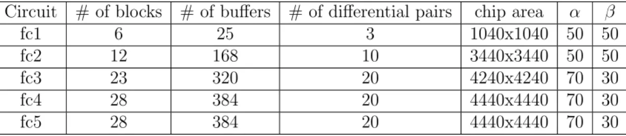
Table 4.1 lists the names of circuits, the number of blocks, the number of buffers, the number of differential pairs, the chip areas and the parameters α and β (also can be defined by the company). The parameter α is the weighting factor of the skew part Φ1 of the objective function Γ, and the β is that of the path delay part
Φ2 of Γ.
Table 4.1: Statistics of the test circuits[2]
Circuit # of blocks # of buffers # of differential pairs chip area α β
fc1 6 25 3 1040x1040 50 50
fc2 12 168 10 3440x3440 50 50
fc3 23 320 20 4240x4240 70 30
fc4 28 384 20 4440x4440 70 30
fc5 28 384 20 4440x4440 70 30
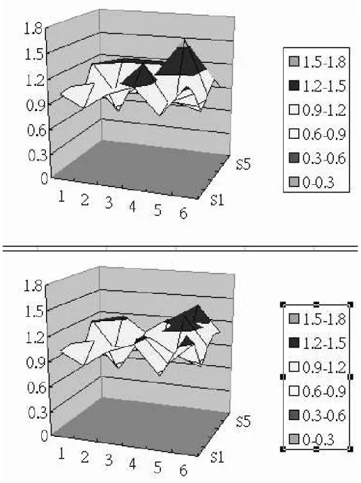
Figure 4.1: Power integrity exhibition before and after concern of case5(fc5). The upper figure has a hot spot that drains more power then the other grids .
eration, additionally. The experiment resultsare shown in Table 4.2 .
As shown in Figure 4.1, our method also obtains better results in power distribu-tion problem. We do not put too many buffer into one grid if the grid’s supporting
Table 4.2: Experimental results of our placement method and [1] where the CPU time of [1] was measured on a 1.2GHz workstation with 8GB memory. This table shows the effectiveness of our approach
Ckt [1] Ours Improvement(%)
Total path delay 17760 18070 -1.74
Max. input skew 120 230 -91.6
Max. output skew 90 180 -100
fc1 Avg. skew of differential pairs - 46.7
Cost Γ 2.01e+06 5.17e+06 -157.2
CPU Time 1s 0.36s
Total path delay 361650 354750 +1.9
Max. input skew 1010 720 +28.7
Max. output skew 1390 740 +46.8
fc2 Avg. skew of differential pairs - 42
Cost Γ 1.66e+08 7.10e+07 +57.2
CPU Time 16s 10.8s
Total path delay 619200 805540 -30.1
Max. input skew 1660 1060 +36.1
Max. output skew 1700 1320 +22.3
fc3 Avg. skew of differential pairs - 116
Cost Γ 4.14e+08 2.25e+08 +45.7
CPU Time 51s 72s
Total path delay 726040 1020220 -40.5
Max. input skew 2190 1200 +45.2
Max. output skew 2380 1500 +36.9
fc4 Avg. skew of differential pairs - 142
Cost Γ 7.54e+08 2.89e+08 +61.7
CPU Time 72s 216s
Total path delay 707430 947830 -33.9
Max. input skew 1730 1130 +34.7
Max. output skew 2160 1120 +48.1
fc5 Avg. skew of differential pairs - 163
Cost Γ 5.57e+08 2.06e+08 +63.0
Chapter 5
Conclusion and Future Work
We have presented a two step heuristic method for the block and I/O buffer place-ment for flip-chip design. This method not only offer a good result in signal skew and differential pairs, but also maintain the power distribution normalization.
For future improvement of our placement method, we can add some more con-straints into out placement algorithm like interconnection between blocks or take Re-Distributed Layer (RDL) into consideration. Connection line from bump to I/O buffer pass by Re-Distributed Layer, but connection line from I/O buffer to core block may pass by some other metal layer. We can model these two kinds of path and develop a better algorithm more associated to the real physical design.
Bibliography
[1] Chih-Yang Peng, Wen-Chang Chao, Yao-Wen Chang, , and Jyh-Herng Wang. “Simultaneous Block and I/O Buffer Floorplanning for Flip-Chip Design.”. In
Asia and South Pacific Conference on Design Automation., pages 24–27, 2006.
[2] Faraday Corp. “Block and Input/Output Buffer Placement for Skew/Delay Minimization in Flip-chip Design”. In Proc. of ACM International
Sym-posium on Physical Design. IC/CAD Contest,Taiwan, 2003. http :
//www.cs.nthu.edu.tw/ cad/cad91/P roblems/P 3/CADcontest2003P3.pdf .
[3] Hao-Yueh Hsieh and Ting-Chi Wang. “Simple Yet Effective Algorithms for Block and I/O Buffer Placement in Flip-Chip Design*”. In IEEE International
Symposium on Circuits and Systems, pages 1879 – 1882, 2005.
[4] Hung-Ming Chen, I-Min Liu, Muzhou Shao, Martin D.F. Wong, and Li-Da Huang. “I/O clustering in design cost and performance optimization for flip-chip design”. In Proceedings. IEEE International Conference on Computer
Design, pages 562 – 567, 2004.
[5] Jinjun Xiong, Yiu-Chung Wong, Egino Sarto, and Lei He. “Constraint Driven I/O Planning and Placement for Chip-package Co-design”. In Asia and South
[6] J. N. Kozhaya, S. R. Nassif, and F. N. Najm. “I/O Buffer Placement Method-ology for ASICs”. In IEEE International Conf. on Electronic, Circuits and
Systems, pages 245–248, 2001.
[7] Audet Jean, D.P. O’Connor, Mike Grinberg, and James P. Libous. “Effect of organic package core via pitch reduction on power distribution performance”. In Proceedings Electronic Components and Technology Conference, pages 1449 – 1453, 2004.
[8] G. Yasar, C. Chiu, R.A. Proctor, , and J.P. Libous. “I/O Cell Placement and Electrical Checking Methodology for ASICs with Peripheral I/Os”. In IEEE
International Symposium on Quality Electronic Design, pages 71 – 75, 2001.
[9] P.H. Buffet, J. Natonio, R.A. Proctor, Y.H. Sun, , and G. Yasar. “Methodology for I/O cell Placement and Checking in ASIC Designs Using Area-Array Power Grid”. In IEEE Custom Integrated Circuits Conference, pages 125–128, 2000. [10] R. Farbarik, X. Liu, M. Rossman, P. Parakh, T. Basso, , and R. Brown. “CAD
Tools for Area-Distributed I/O Pad Packaging”. In IEEE Multi-Chip Module
Conference, pages 125–129, 1997.
[11] P.S. Zuchowski, J.H. Panner, D.W. Stout, J.M. Adams, F. Chan, P.E. Dunn, A.D. Huber, , and J.J. Oler. “I/O Impedance Matching Algorithm for High Performance ASICs,”. In IEEE International ASIC Conference and Exhibit, pages 270–273, 1997.
[12] C. Tan, D. Bouldin, , and P. Dehkordi. “Design Implementation of Intrinsic Area Array ICs”. In Proceedings 17th Conference on Advanced Research in
[13] R.J. Lomax, R.B. Brown, M. Nanua, , and T.D. Strong. “Area I/O Flip-Chip Packaging to Minimize Interconnect Length,”. In IEEE Multi-Chip Module
Conference,, pages 2–7, 1997.
[14] S. N. Adya, I. L. Markov, , and P. G. Villarrubia. “On whitespace in mixed-size placement and physical synthesis”. In Proceedings of IEEE/ACM Int. Conf. on
Computer-Aided Design, pages 311–318, 2003.
[15] A. R. Agnihotri, M. C. Yildiz, A. Khatkhate, A. Mathur, S. Ono, and P. H. Madden. “Fractical cut: improved recursive bisection placement”. In
Pro-ceedings of IEEE/ACM Int. Conf. on Computer-Aided Design,, pages 307–310,
2003.
[16] A. E. Caldwell, A. B. Kahng, and I. L. Markov. “Can recursive bisection alone produce routable placement?”. In Proc. of ACM/IEEE Design Automation
Conf., pages 477–482, 2000.
[17] T. Chan, J. Cong, and K. Sze. “Multilevel generalized force-directed method for circuit placement”. In Proc. of ACM International Symposium on Physical
![Figure 1.1: Example layout of the flip-chip[2].](https://thumb-ap.123doks.com/thumbv2/9libinfo/8381601.178219/13.918.191.702.238.940/figure-example-layout-of-the-flip-chip.webp)
![Figure 2.1: Example of path delay calculation, the orders from left to right are bump, I/O buffer and block[2].](https://thumb-ap.123doks.com/thumbv2/9libinfo/8381601.178219/17.918.220.766.175.325/figure-example-delay-calculation-orders-right-buffer-block.webp)
![Table 4.2: Experimental results of our placement method and [1] where the CPU time of [1] was measured on a 1.2GHz workstation with 8GB memory](https://thumb-ap.123doks.com/thumbv2/9libinfo/8381601.178219/30.918.139.758.340.1033/table-experimental-results-placement-method-measured-workstation-memory.webp)