I
國
立
交
通
大
學
光電工程學系碩士班
碩
士
論
文
透明非晶態氧化鋅錫搭配無銦電極之薄膜電晶體
Transparent Amorphous Zn-Sn-O Thin Film Transistors
with Indium Free Electrodes
研 究 生:許博凱
指導教授:謝漢萍 教授
黃乙白
副教授
II
透明非晶態氧化鋅錫搭配無銦電極之薄膜電晶體
Transparent Amorphous Zn-Sn-O Thin Film Transistors
with Indium Free Electrodes
研 究 生:許博凱 Student:Po-Kai Hsu
指導教授:謝漢萍 Advisor:Han-Ping D. Shieh
黃乙白
Yi-Pai Huang
國立交通大學 電機學院
光電工程學系碩士班
碩 士 論 文
A ThesisSubmitted to Institute of Electro-Optical Engineering College of Electrical and Computer Engineering
National Chiao Tung University in Partial Fulfillment of the Requirements
for the Degree of Master in
Electro-Optical Engineering June 2012
Hsinchu, Taiwan, Republic of China
I
透明非晶態氧化鋅錫搭配無銦電極之薄膜電晶體
學生:許博凱 指導教授: 謝漢萍教授
黃乙白副教授
國立交通大學電機學院 光電工程學系碩士班
摘 要
由於銦價不斷的上漲,氧化薄膜電晶體中無銦的材料逐漸受到重視。本文著 墨於無銦的非晶態氧化鋅錫薄膜電晶體的薄膜特性、光學特性、電性特性、穩定 度以及抗蝕刻特性的研究,同時也與氧化銦鎵鋅薄膜電晶體做比較與討論。為了 實現整個元件都無銦,在透明電極材料上使用氧化鋁鋅做為源極與漏極搭配氧化 鋅錫薄膜電晶體的特性也做了完整的研究與比較。 實驗結果顯示氧化鋅錫電晶體因為有低的有效電子質量與較高的載子濃度, 所以有較高的載子移動率,且在穩定度上因為氧化鋅錫有較大的電負度,所以在 正偏壓應力與高溫下有較高的穩定性。而抗刻蝕刻力的結果顯示氧化鋅錫的抗蝕 刻性是氧化銦鎵鋅的 8.4 倍,這將有利於濕式蝕刻的製程。本研究的結果指出無 銦的非晶態氧化鋅錫薄膜電晶體有潛力作為高性能非金態氧化物的薄膜電晶 體。II
Transparent Amorphous Zn-Sn-O Thin Film
Transistors with Indium Free Electrodes
Student: Po-Kai Hsu Advisor: Prof. Han-Ping D. Shieh Prof. Yi-Pai Huang
Dept. of Photonics & Institute of Electro-Optical Engineering National Chiao Tung University
Abstract
Oxide thin film transistors (TFTs) based on Indium-free materials are in high demand due to the price of In increase substantially. To solve those issues, zinc oxide (ZnO) based semiconductor materials are introduced and studied. Present study aims to develop the In-free metal oxide TFTs and discusses the characteristics of amorphous Zn-Sn-O (a-ZTO) TFTs, including thin film qualities, optical properties, electrical properties, stabilities, and etching resistance. Also, the comparisons of a-ZTO and amorphous In-Ga-Zn-O (a-IGZO) TFTs are presented. To realize the In-free TFTs, the
III
a-ZTO TFTs with transparent conductive oxide Al-Zn-O (AZO) is used as source and drain electrodes.
The electrical results demonstrate that the mobility of a-ZTO TFT is higher than a-IGZO TFT, because a-ZTO has the lower effective mass and the higher carrier concentration. A-ZTO has the higher electronegativity in stronger metal oxide bonding than a-IGZO that result in better stability under a temperature bias stressing. A-ZTO has a factor of 8 higher in etching resistance compared to that of a-IGZO, thus, more easily forming high quality patterns definition in wet etching process. These results imply that a-ZTO TFT is promising to be high performance In-free TFTs.
IV
誌謝
經過一番的努力,碩士的生涯總算要告一段落了。很慶幸能夠在謝漢萍老師 和黃乙白老師的實驗室中做研究,實驗室提供了充足的資源,老師以及學姐也給 予了很大的自由度可以做自己想做的實驗。研究的過程中學習到了很多關於發掘 問題、研究問題、解決問題的能力,與別人合作的過程中也學會了很多團隊精神 與待人處事的道理。感謝黃老師當初在我還是備取的時候大膽的收我進實驗室; 感謝謝老師在投影片製作的指導和英文口與簡報的要求,讓我在這方面的能力進 步不少。 在研究中要特別感謝韻竹學姐這兩年的指導與鼓勵,在實驗上時常的給予有 幫助的意見且在寫論文的階段不厭其煩的修定我的論文,真的非常的感謝。同時 也感謝來台遊學的詹博、奕智學長、致維哥、大頭、立偉等學長提供許多意見與 教導,也感謝學弟小黑在實驗上的幫忙。感謝張綺、拉拉讓實驗室添增了許多色 彩;感謝白諭和冋務讓我的研究生活充滿了許多樂趣,也謝謝實驗室的所有同學 和學弟們,與大家在一起的時光所編織回憶,我永遠會掛念在心的。最後感謝家 人的栽培與付出。碩畢以後期許自己能夠做一個負責任且可靠的人,以回報愛我 與我愛的人。V
Table of Contents
摘 要 ... I
Abstract ... II
誌謝 ... IV
Table of Contents ... V
Figure Captions ... VIII
Table Captions... XII
Chapter 1 ... 1
1-1. Background of Thin Film Transistors (TFTs) ... 1
1-2. Development of TFTs ... 4
1-3. Application of TFTs ... 8
1-4. Motivations and Objective ... 11
1-5. Thesis Organization ... 14
Chapter 2 ... 15
2-1. Introduction ... 15
VI
2-3. Electrical Properties of TFTs ... 18
2-4. Carrier Transporting Mechanism in AOS ... 18
2-5. Methods of Parameter Extraction ... 20
2-5.1 Determination of the Threshold Voltage (Vth) ... 21
2-5.2 Determination of the Sub-Threshold Swing (SS) ... 22
2-5.3 Determination of Field-Effect Mobility (μFE) ... 22
2-5.4 Ion/Ioff ... 23
2-6. Summary ... 23
Chapter 3 ... 25
3-1. Introduction ... 25
3-2. Principle of Sputtering System ... 25
3-3. Device Fabrication Processes ... 27
3-3.1 Substrate Cleaning... 28
3-3.2 Active Layer Deposition ... 28
3-3.3 Electrode Deposition ... 29
3-3.4 Post Annealing Process ... 29
3-4. Thin Film Analysis ... 32
3-4.1 Measurement of Optical Properties ... 32
3-4.2 X-Ray Diffraction (XRD) ... 33
3-4.3 Surface Morphology ... 33
3-4.4 Carrier Concentration and Mobility of Thin Films... 34
3-4.5 Etching Rate ... 36
3-5. Device Measurements ... 37
3-5.1 Electrical Characteristics ... 37
VII
3-6. Summary ... 38
Chapter 4 ... 39
4-1. Introduction ... 39
4-2. Analysis of Thin Films ... 39
4-2.1 Deposition Conditions ... 39
4-2.2 Optical Properties ... 41
4-2.3 Crystalline Phase and Surface Morphology ... 44
4-2.4 Hall Measurement ... 47
4-3. Comparisons of a-ZTO and a-IGZO TFTs ... 47
4-3.1 Electrical Characteristics of a-ZTO TFTs ... 47
4-3.2 Transfer Characteristics under Positive Bias Stressing (PBS) ... 50
4-3.3 Transfer Characteristics under Temperature Stressing (TBS) ... 53
4-3.4 Transfer Characteristics under Negative Bias Stressing (NBS) ... 56
4-3.5 Summary of Active Effects ... 58
4-4. Comparisons of a-ZTO TFTs with ITO and AZO Electrodes ... 60
4-4.1 Electrical Characteristics of a-ZTO TFTs with In-Free Electrodes ... 60
4-4.2 Transfer Characteristics under Bias Stressing ... 64
4-4.3 Summary of Electrodes Effects ... 66
4-5. Etching Resistance ... 68
Chapter 5 ... 71
5-1. Conclusions ... 71
5-2. Future work ... 74
VIII
Figure Captions
Fig. 1-1 The schematic of a TFT. ... 3
Fig. 1-2 Four kinds of structures for TFTs. ... 3
Fig. 1-3 Cross section structure diagram of the TFT-LCD panel [23]. ... 9
Fig. 1-4 The circuit schematic of an AMOLED pixel [24].S ... 10
Fig. 1-5 Photographs of (a) 6.5 inch flexible full-color top emission AMOLED panel with a-IGZO TFTs as back plane [25] and (b) 32 inch prototype OLED TV driven by a-IGZO TFTs [26]. ... 11
Fig. 1-6 Price charts of (a) indium, (b) zinc, (c) tin, and (d) aluminum, respectively [27]. ... 13
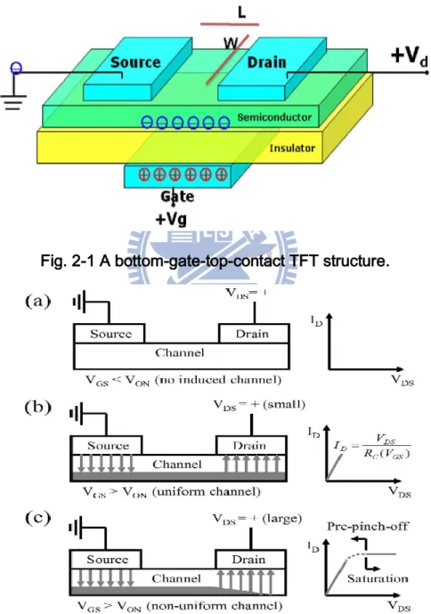
Fig. 2-1 A bottom-gate-top-contact TFT structure. ... 17
Fig. 2-2 Operation principle of TFTs (a) off state region, (b) linear region, and (c) saturation region, respectively [30]. ... 17
Fig. 2-3 Schematic of orbital drawing of electron pathway (conduction band bottom) in conventional silicon-base semiconductor and ionic oxide semiconductor [32]. ... 20
IX
Fig. 2-4 Conventional n-type TFTs transfer characteristics. ... 21
Fig. 3-1 Typical RF sputtering system. ... 26
Fig. 3-2 The Sputtering system in NCTU. ... 26
Fig. 3-3 Atmospheric anneal furnace. ... 30
Fig. 3-4 Flowchart of a-ZTO TFTs fabrication. ... 31
Fig. 3-5 (a) UV-VIS spectrophotometer at NCTU and (b) schematics of UV-VIS spectrophotometer. ... 32
Fig. 3-6 (a) AFM and (b) SEM in NCTU. ... 34
Fig. 3-7 Hall Effect Measurement System in NCTU. ... 35
Fig. 3-8 Keithley 4200 of NCTU. ... 37
Fig. 4-1 Deposition rate of a-ZTO varied with different sputtering (a) pressure and (b) power. ... 41
Fig. 4-2 (a) Transmittance and (b) Optical band gap of 50-nm thick a-ZTO and a-IGZO film. ... 43
Fig. 4-3 XRD results of (a) ZTO and (b) IGZO thin films. ... 45
Fig. 4-4 (a) Step height of a-ZTO thin film, roughness of (b) a-ZTO and (c) a-IGZO. ... 45
X
Fig. 4-5 3D surface morphology of (a) a-ZTO and (b) a-IGZO. ... 46 Fig. 4-6 SEM results: surface morphology of (a) a-ZTO and (b) a-IGZO thin film. ... 46 Fig. 4-7 Transfer characteristics of a-ZTO and a-IGZO TFTs in saturation region where VDS=10V. ... 49
Fig. 4-8 Transfer characteristics of (a) a-ZTO and (b) a-IGZO TFT in saturation region VDS=10 V under positive bias stressing VDS=VGS=20 V at RT in the dark
box. ... 52 Fig. 4-9 Vth, μFE, SS, and Ion/Ioff shift versus stressing time for a-ZTO/a-IGZO
TFTs by a positive bias stress. ... 52 Fig. 4-10 Transfer characteristics of (a) a-ZTO and (b) a-IGZO TFT were stressed at 80℃ with VGS= 20 V and VDS= 20 V. ... 55 Fig. 4-11 Vth, μFE, SS, and Ion/Ioff shift versus stressing time for a-ZTO/a-IGZO
TFTs by a temperature stressing. ... 55 Fig. 4-12 Transfer characteristics of (a) a-ZTO and (b) a-IGZO TFT in saturation region VDS=10 V under negative bias stress VGS= -20 V. ... 57
XI
TFTs by a negative bias stress. ... 58 Fig. 4-14 Transmittance of AZO and ITO. ... 63 Fig. 4-15 Transfer characteristics of a-ZTO TFTs with ITO and AZO electrodes in saturation region VDS=10V. ... 64
Fig. 4-16 Vth, μFE, SS, and Ion/Ioff shift versus stressing time for a-ZTO TFT with
ITO/ AZO electrodes under positive bias stressing. ... 65 Fig. 4-17 Vth, μFE, SS, and Ion/Ioff shift versus stressing time for a-ZTO TFT with
ITO/ AZO electrodes under temperature stressing. ... 65 Fig. 4-18 Vth, μFE, SS, and Ion/Ioff shift versus stressing time for a-ZTO TFT with
ITO/ AZO electrodes under temperature stressing. ... 66 Fig 4-19 The average transmittance of (a) a-ZTO and (b) a-IGZO etched thin films. ... 69 Fig 4-20 Etching rate of a-ZTO and a-IGZO thin films. ... 70 Fig 5-1 Process flowchart of the future improvement. ... 78
XII
Table Captions
Tab. 1-1 The characteristics of p-Si, a-Si, organic, and AOS materials ... 8 Tab. 4-1 Optical properties of a-ZTO and a-IGZO thin film. ... 43 Tab. 4-2 Hall measurement of a-ZTO and a-IGZO thin film. ... 47 Tab. 4-3 Comparisons of electrical performance of a-ZTO and a-IGZO TFTs. ... 60 Tab. 4-4 Resistivity and work function of ITO and AZO. ... 63 Tab. 4-5 Comparisons of electrical performance of a-ZTO TFT with ITO/AZO electrodes. ... 67 Tab. 5-1 Thin-film properties of a-ZTO and a-IGZO thin film. ... 73 Tab. 5-2 Electrical properties of a-ZTO and a-IGZO TFTs with AZO/ITO electrodes. ... 74
1
Chapter 1
Introduction
1-1. Background of Thin Film Transistors (TFTs)
In this technological era, a variety of sophisticated electronic components are growing popular. The development of flat panel displays is particularly important because displays play a bridge between human and electronic components. In order to achieve high-performance displays, such as ultra definition (3840x2160) TV [1], transparent displays [2], and flexible displays [2], the active matrix driver circuit and the backlight module need to improve.
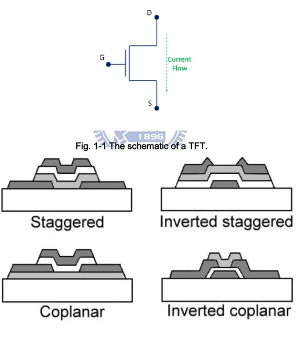
A thin film transistor (TFT) is a metal-oxide-semiconductor field effect transistor (MOSFET) fabricated on an insulator substrate by employing all thin film constituents. Conventional TFTs are composed of a semiconductor layer, a gate insulator layer, and electrode terminals. The TFTs are particular form of field-effect transistors by depositing the active layer with a thin film semiconductor. A TFT device consisted of three terminals is shown in Figure 1-1. The gate (G) terminal acts as a switch to control the transistor to open or close in a circuit then, the current flows from drain (D) to source (S) which is
2
originated from the drift of electron carriers. There are four structures for TFTs, including staggered, inverted staggered, coplanar, and inverted coplanar TFTs, as shown in Figure 1-2. The classification of the structures is convenient to define by the stacked order of the gate electrode, gate insulator (GI), active layer, and source/drain electrodes.
The world's first TFT using cadmium sulfide (CdS) as active layer has been successfully developed by Weimer in 1962 [3]. Afterward, other kinds of semiconductors such as cadmium selenide (CdSe) [4] and indium antimonide (InSb) [5] as the channel materials were used in the TFT devices.
At 1970s, liquid crystal displays (LCDs) were developed and the concept of active-matrix drive circuit was emerged; therefore, TFT technology was then attracted a lot of the attention of researchers. In 1979, amorphous silicon (a-Si) as channel layer of TFTs technology obtained widespread attention and commercial applications [6,7]. In the 1990s, the organic semiconductor as active layer (OTFTs) began to develop and be utilized in active-matrix organic light-emitting diode displays (AM-OLEDs) [8,9,10,11].
TFTs researches were developed rapidly over the past decade including the investigations of device performance, production cost, and manufacturing processes. Researchers focus gradually shifted from a-Si to other materials,
3
for example, amorphous oxide semiconductors (AOSs). The AOS TFTs have many benefits including high mobility, low process temperature, high transmittance, and large-area uniformity. In response to TFTs having large number of applications on the flat panel displays, the transparent conducting oxides (TCOs) as the TFT’s electrode were discussed.
Fig. 1-1 The schematic of a TFT.
4
1-2. Development of TFTs
The development history of TFT had been investigated over 50 years. This section introduces the development of channel materials in TFTs, including the Si TFTs, OTFTs, and the AOS TFTs.
Silicon Semiconductors
The course of development of Si TFT devices has experienced monocrystalline silicon (c-Si) [12], a-Si [6,7], polycrystalline silicon (p-Si) [13], and microcrystalline silicon (μ-Si) [14]. The c-Si is not conducive to apply on microelectronics technology because of the nature of hard and brittle at room temperature. A hydrogenated a-Si (a-Si:H) exhibits the large area uniformity for TFTs, solar cells, sensors, and other electronic devices. A-Si is the mainstream material for present TFTs. However, there are some issues of a-Si TFTs in the active-matrix-driven devices. The large resistance of on-state and the low field-effect mobility for a-Si TFTs do not match the requirement for future displays [15]. On the other hand, stability should be improved for a-Si TFT since it is easy to form the photo-carrier under visible light [16]. To solve these difficulties, p-Si as the substitute of a-Si is proposed. Heave doping is easy for p-Si, so ion implantation was used in p-Si TFTs to form the heavily
5
doped p-Si source and drain electrodes. The parasitic capacitance between drain, source, and gate can be reduced by self-alignment technique, resulting in higher field-effect mobility, faster response time. Nevertheless, p-Si TFTs have some issues including large off-state current, low uniformity, and high process temperature.
Organic Semiconductors
The first organic TFTs were demonstrated by Koezuka in 1978 [17]. Compared with inorganic TFTs, organic semiconductor materials possesses the benefits such as simple processes, light weight, low cost and flexibility.
The current issues of OTFTs are the existence of a large number of defect states thich cause low carrier concentration, the impact of the external environment results in lower stability, etc [18]. These drawbacks of OTFTs limit the applications in the display industry.
Amorphous Oxide Semiconductors
In recent years, in order to solve the issues of Si TFTs and OTFTs, the amorphous oxide semiconductor (AOS) TFTs was developed.AOS TFTs have several features that are attractive for flat-panel displays and large-area
6
integrated circuits [19]. The advantageous of AOS TFTs are summarized as follows:
1. Wide processing temperature window : By choosing an appropriate chemical composition, AOSs form stable amorphous phases with high crystallization temperatures (> 500 °C); and, the various electrical properties can be achieved by adjusting the process temperature.
2. Low processing temperature : AOS TFTs exhibit satisfactory operation characteristics even fabricated at room temperature, and this will facilitate the production of flexible displays.
3. Low operating voltage : Oxides have electronic structures specific to the ionic chemical bonds, and they form much fewer defect states in the band gap compared to conventional covalent semiconductors such as Si. The lower defect density allows a small subthreshold swing (SS) value of 0.1 V/decade and low operation voltages of < 5 V.
4. Large carrier mobility : AOS TFTs exhibit the field effect mobility above 10 cm2/Vs, which is more than one order of magnitude compared to traditional
a-Si TFTs.
5. Simple electrode structure and low off current : Si-based field-effect transistors require a p–n junction for the source and drain electrodes to
7
suppress inversion operation and the consequent increase the off current. Since AOS TFTs do not exhibit inversion p-channel operation, simple metallic contacts may be used for source and drain electrodes without increasing the off current.
6. Easy of fabrication : The features such as the possibility of low-temperature fabrication, insensitivity to gate insulator, the simple electrode structure and the wide flexibility of processing temperature, allow easy fabrication of AOS TFTs. The conventional sputtering methods can be adopted for AOS TFTs [20, 21].
7. Excellent uniformity and surface flatness : AOS TFTs exhibit excellent uniformity and surface flatness (< 0.3 nm) owing to the amorphous structure, and this property facilitates the production of large-size displays [22].
8. High transparency in visible light : most of the AOS materials have high optical band gap (> 2.6 eV) which have more than 80% transmittance in visible light, and this facilitates the production of transparent displays.
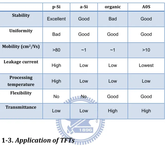
Due to above-mentioned advantages, the AOS TFTs are promising for next-generation displays. The comparisons of a-Si TFTs, p-Si TFTs, OTFTs, and AOS TFTs are summarized in Table 1-1.
8
Tab. 1-1 The characteristics of p-Si, a-Si, organic, and AOS materials
p-Si a-Si organic A0S
Stability
Excellent Good Bad Good
Uniformity
Bad Good Good Good
Mobility (cm2/Vs)
>80 ~1 ~1 >10
Leakage current
High Low Low Lowest
Processing
temperature High Low Low Low
Flexibility
No No Good Good
Transmittance
Low Low High High
1-3. Application of TFTs
The TFTs array driven LCD (TFT-LCD) technology is developing rapidly in recent years, TFT-LCD becomes the mainstream technology for the display industry. The cross section structure shown in Figure 1-3 is a standard TFT-LCD panel. In the each pixel of TFTs array, ITO electrode connected to drain, signal line and gate. In the display, a TFT plays the role of the switch which adjusts the input voltage and changes the transmittance of the liquid crystal, thus achieving the purpose of image display. Contrast, brightness,
9
color, gray scale, power consumption, and response time of LCDs are improved by using the active matrix backplane.
Fig. 1-3 Cross section structure diagram of the TFT-LCD panel [23].
The circuit schematic of OTFT-driven AMOLED pixel is demonstrated in Figure 1-4 [24]. The circuit structure includes two TFTs and one capacitor Cs,
called an OLED pixel unit. The TFT1 is a switching device to control a single
pixel and the TFT2 as drive device to control current flow through OLED is
used to adjust the brightness. Therefore, to achieve high brightness requirements, developing high mobility TFT is an effective way.
10
Fig. 1-4 The circuit schematic of an AMOLED pixel [24].
In last decade, AOS TFTs with lots of advantages are developed by the displays industry. Manufacturers demonstrated different products using oxide TFTs as shown in Figure 1-5. Samsung Mobile Display reported a 6.5 inch flexible AMOLED driven by a-IGZO TFTs. The TFTs deposited on polyimide substrate shows no deterioration when bended down to radius (R) = 3mm [25], and the annealing was conducted at 220 . AU Optronics (AUO) demonstrated 32 inch prototype OLED TV using a-IGZO TFTs at FPD International 2011 as show in Figure 1-5 [26]. These prior arts indicated that oxide TFTs-based devices can realize next generation displays.
11
(a) (b)
Fig. 1-5 Photographs of (a) 6.5 inch flexible full-color top emission AMOLED panel with a-IGZO TFTs as back plane [25] and (b) 32 inch prototype OLED TV driven by a-IGZO TFTs [26].
1-4. Motivations and Objective
There are some issues of a-Si TFTs, p-Si TFTs, and OTFTs, including low mobility, high fabrication temperature, low stability, and high cost that cannot meet the demands of high-performance displays. Therefore, the development of the oxide TFT devices has become important because it lays the foundation for future high-performance displays.
Indium-gallium-zinc-oxide (IGZO) is the most commonly discussed AOS
material. However, a-IGZO has the drawback of being expensive indium (In) which is a rare (6000 metric tons worldwide in 2006) and expensive element.
12
In addition, as the demand of In increases for flat-panel displays and solar cells, causing the price increase substantially. Figure 1-6 shows the price charts of In, Zn, Sn, and Al, respectively [27]. As can be seen in Figure 1-6, the price of In is around 25 times higher than the price of Sn. Moreover, some studies report that the price of In will exceed 2000 USD/kg in the near future [27]. For these reasons, the In-free and low cost substitute materials: zinc oxide (ZnO) and tin oxide (SnO2) have attracted many attentions recently. Previous studies
presented that Zn-Sn-O (ZTO) has high transmittance, wide band gap, good uniformity and high mobility; thus, a-ZTO has the potential as a material to replace a-IGZO. The present study aims to develop the non-rare earth metal oxide TFTs, discussions of the characteristics of a-ZTO TFTs, including thin film qualities, optical properties, electrical properties, and stabilities. The comparisons with the a-IGZO TFTs are presented in this thesis. Additionally, to replace the In rich based TCO, ZnO based conductors such as AZO proposed as alternative materials are also studied to construct the In-free TFTs.
13
(a) (b)
(c) (d)
Fig. 1-6 Price charts of (a) indium, (b) zinc, (c) tin, and (d) aluminum, respectively [27].
Another issue of a-IGZO is etching resistance. Etching process is much reliable and preferred for generating fine patterns in electronics manufacturing. In contrast to dry etching, wet etching results in higher performance, lower cost, and larger area in mass-production [28]. In a process of fabricating AOS-based TFTs that are generally composed of multi-layers of transparent oxides to form a “thoroughly transparent” electronic device, the etching rates of those layers to be patterned individually must be known in advance. However, some
14
researches reported that etching resistance of a-IGZO is too low [29], which can result in lower etching rate selectivity between a-IGZO and TCOs electrodes. To solve this issue, we proposed and studied the etching resistance of a-ZTO to improve the low etching selectively of AOS TFTs.
1-5. Thesis Organization
This thesis is organized as follows: The operation principle of TFTs, electrical properties of TFTs, carrier transporting mechanism in AOS, and the extraction method of TFTs device parameters are described in Chapter 2. The experimental schemes and methods are presented in Chapter 3. In Chapter 4, the optical properties of a-ZTO, thin film transfer characteristics including stabilities of a-ZTO TFTs, and etching resistance of a-ZTO thin film are discussed. The comparisons of a-ZTO/a-IGZO and ITO/AZO TFTs are also proposed, respectively. Finally, conclusions and future works are summarized in Chapter 5.
15
Chapter 2
Principle and Characterization
2-1. Introduction
The operation principles of TFTs are introduced. The electrical properties of TFTs will then be illustrated. Next, the carrier transporting mechanism in AOS is presented. Finally, the extraction method of electrical parameters such as threshold voltage (Vth), sub-threshold swing (SS), field-effect mobility (μFE),
and Ion/Ioff are defined.
2-2. Operation Principle of TFTs
The operation principle and the structure of TFTs are similar to the metal-oxide-semiconductor field-effect transistors (MOSFETs). The TFTs are categorized to n-type and p-type TFTs, and the majority carriers are electrons in the n-type channel. On the other hand, the majority carriers are holes in the p-type channel. To elucidate the operation mechanism, an n-type and bottom-gate-top-contact TFT configuration is plotted in Figure 2-1.
16
in the channel layer. Since the intrinsic carrier concentration is low; the electrical conductivity of the channel layer and the current between source and drain are very small. A lot of electrons at the surface between gate insulator and channel layer are induced when exerting a positive bias on gate. Meanwhile, conductivity of the semiconductor is improved greatly to form a conductive channel. On the other hand, exerting a negative bias on gate depletes the carriers at channel layer. By applying different gate voltage, the interface of channel layer and gate insulator can be either charge accumulation or also charge depletion. Thus, adjusting the different gate voltage may modulate the carrier concentration in channel layer.
When a bias voltage exerted to gate (VGS) is less than turn-on voltage
(Von), channel layer does not form a conductive channel, and hence no current
is generated. It is called the off state as shown Figure 2-2 (a) [30]. When VGS is
larger than Von, carriers in channel layer are induced by electric field that are
forming a conductive channel and generating the drain to source current (IDS).
When the drain voltage (VDS) is small, the channel is in the accumulated state
that is called linear region as can be seen in Figure 2-2 (b). When VDS
increased gradually, the thickness of channel becomes asymmetric due to the electric field effect, and the thickness of channel in drain end is smaller than
17
the one in source end. When VDS reaches the saturation voltage, the carriers
disappear and channel is just pinch-off in drain end. If VDS is increased over
the saturation voltage, the TFT is in saturation region as illustrated in Figure 2-2 (c).
Fig. 2-1 A bottom-gate-top-contact TFT structure.
Fig. 2-2 Operation principle of TFTs (a) off state region, (b) linear region, and (c) saturation region, respectively [30].
18
2-3. Electrical Properties of TFTs
The standard parameters of the TFTs include channel width (W), channel length (L), and capacitance per unit area of the gate insulator (COX). In the
linear region (VDS VGS Vth) [31], the drain current is directly proportional
to the drain voltage and can be written as:
(2-1)
where μFE is field-effect mobility. Vth is denoted as the smallest applied gate
voltage that causes a non-negligible increasing in drain current for a given drain voltage. When the drain voltage increases and exceeds the relational expression of VDS VGS Vth, the drain current is constant with increasing
the drain voltage and this condition is called the saturation region. The drain current can be expressed by Eq. 2.2.
– (2-2)
2-4. Carrier Transporting Mechanism in AOS
The mobility of a-Si:H (~1 cm2V-1s-1) [6,7] is much smaller than that of
single crystalline Si (>80 cm2V-1s-1) [12,13] due to the intrinsic chemical
19
semiconductors, such as a-Si:H, consist of strongly directive sp3 orbitals. The
bond angle fluctuation significantly alters the electronic levels, causing high density of deep tail-states, as shown in Figure 2-3 [32].
In contrast, transparent oxides constituting of heavy post transition metal cations with the (n-1) d10ns0 electron configuration, where n ≥ 5, are the transparent AOS (TAOS) candidates having large mobilities comparable to those of the corresponding crystals. The electron pathway in oxide semiconductor is primarily composed of spatially spread ns orbitals with an isotropic shape, as shown in Figure 2-3. The direct overlap among the neighboring ns orbital is possible. The degree of overlap of the ns orbital is insensitive to the distorted metal-oxygen-metal bonding. This feature shows why the Hall mobility of AOS is similar to the corresponding crystalline phase, even under the room temperature deposited of thin-films.
20
Fig. 2-3 Schematic of orbital drawing of electron pathway (conduction band bottom) in conventional silicon-base semiconductor and ionic oxide semiconductor [32].
2-5. Methods of Parameter Extraction
The methods of typical parameters extraction such as threshold voltage (Vth), subthreshold swing (SS), On/Off current ratio (Ion/Ioff) and field effect
mobility (μFE) from device characteristics are described. The IDS is plotted
21
will then be described in detail.
Fig. 2-4 Conventional n-type TFTs transfer characteristics.
2-5.1 Determination of the Threshold Voltage (V
th)
Plenty of methods are available to determine Vth which is one of the
most important parameters of semiconductor devices. The intercept of the extend line in -VG diagram is adopted and based on the transformation formula of ID-VG in saturation region as shown in Eq. 2-2. Vth depend on the
conductive degree of channel layer, trap density in the interface of channel/gate insulator layer, and the contact quality of electrodes/channel layer.
22
2-5.2 Determination of the Sub-Threshold Swing (SS)
Subthreshold swing (SS) is a typical parameter to describe the control ability of gate toward channel which is the speed of turning the device on and off. It is defined as the gate voltage required to increase and decrease the drain current by one order of magnitude. SS is related to the process, and it is irrelevant to device dimensions. SS can be lessened by substrate bias since it is affected by the total trap density including interfacial trap density and bulk density. In this study, SS is defined as one-half of the gate voltage required to decrease the threshold current by two orders of magnitude (from 10-7A to
10-9A). The threshold current is specified as the drain current when the gate
voltage is equal to Vth. SS is evaluated from the TFTs transfer characteristic in
the sub-threshold regime, using the following formula:
(2-3)
2-5.3 Determination of Field-Effect Mobility (μ
FE)
The field-effect mobility (μFE) means the average moving speed of the
carrier under electric field. μFE indicates the ability of carrier mobility in
semiconductors. Typically, μFE is derived from the transconductance (gm) at
low drain voltage (VD = 0.1 V) [33]. If VD is much smaller than VG – Vth, then VD
23 Eq. 2-4. (2-4) Transconductance is defined as
(2-5) Thus,
(2-6)
2-5.4 I
on/I
offIon/Ioff is defined as the ratio of maximum on-current and minimum
off-current of drain current (ID), which illustrates the modulation capability of
the device current. High Ion/Ioff represents not only the large turn-on current but
also the small off current (leakage current). Ion/Ioff affects AMLCD gray levels
(the bright to dark state number) directly. There are many factors affect Ion/Ioff
such as carrier concentration, dimension of channel width/length, interface state, and ohmic contact.
2-6. Summary
The a-ZTO thin film is an In-free material that has a potential to reduce the cost. Therefore, a-ZTO TFTs have the potential to replace a-IGZO TFTs. For
24
practical applications, the thin film characteristics and electrical properties must be studied and analyzed.
25
Chapter 3
Experimental Methods
3-1. Introduction
The device fabrication and processing parameters are described. The principle of RF sputtering system will be described. Afterward, the fabrication facilities and the process flow are introduced. At last, the analytical methods and tools are illustrated.
3-2. Principle of Sputtering System
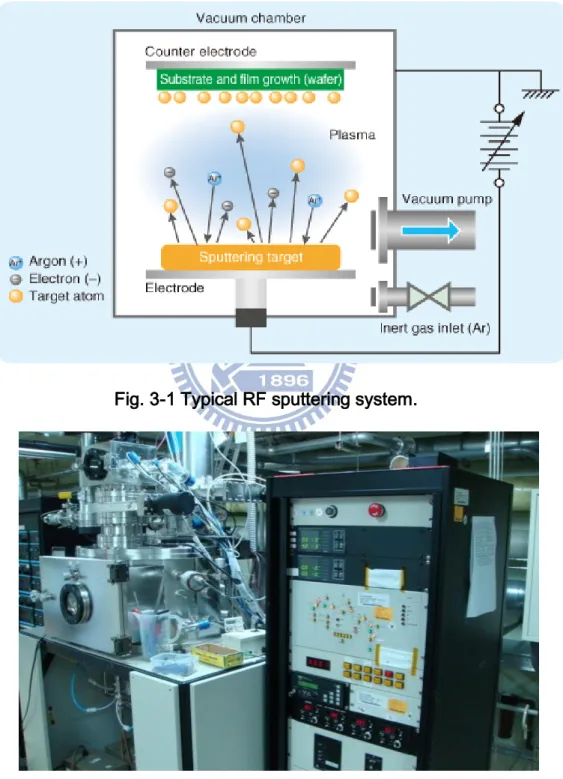
Magnetron radio frequency (RF) sputtering is the most important tool of thin film deposition in this work. RF sputtering uses high-frequency power to prevent the charges accumulated in the target. Furthermore, the magnetron is used to modulate the electron moving path, which improves plasma collision frequency.
The RF sputtering can be used to sputter both insulator and conductive targets, since the charge does not build up on the surface of the target. A schematic diagram of a typical RF sputtering system is shown in Figure 3-1.
26
The high vacuum sputtering system in NCTU is placed in class 10K clean room as shown in Figure 3-2.
Fig. 3-1 Typical RF sputtering system.
27
Firstly, the substrate is placed in a vacuum chamber with the source material, named a target, and the working gases (such as argon (Ar) or oxygen (O2)) are introduced at low pressure (typically between 1mTorr and 10 mTorr).
Gas plasma is struck using an RF power source, causing the gas to become ionized. The ions are accelerated towards the surface of the target, causing atoms of the source material to break off from the target in vapor form and condense on the substrate. A lower working pressure increases the mean free path which results in the deposited species having more energy to diffuse along the substrate surface in order to find the lowest energy state possible.
3-3. Device Fabrication Processes
In this experiment, an n-type (antimony doping) Si wafer with 100nm thick thermal SiO2 was selected to represent the gate electrode and insulator layer,
respectively. The active layer and source/drain electrodes were deposited by the RF magnetron sputter at room temperature (RT), respectively. The flowcharts of the fabrications are shown in Figure 3-4 and the deposition details of each procedure are described in the following sections.
28
3-3.1 Substrate Cleaning
Firstly, the 3cm x 3cm wafer was cleaned by DI water for 10 minutes. Then, the wafer is placed in a container with acetone and ultrasonic vibration for 30 minutes to remove organic pollution. The wafer was then placed in another container with isopropanol (IPA) and ultrasonic vibration for 30 minutes to remove acetone. Finally, nitrogen (N2) jet was used to purge dry the
wafer and then put the wafer in an oven at 120 ゚C for 10 minutes.
3-3.2 Active Layer Deposition
N-type (antimony doping) silicon wafer as the gate electrode with 100 nm thick thermal SiO2 as the gate insulator layer were used to reduce the gate
insulator interface trapping issue. Shadow masks were used to define the pattern of active layer. Meanwhile, the active layer of 50-nm-thick a-ZTO and a-IGZO were deposited by RF magnetron sputtering with the ZnSnO3 target
(ZnO : SnO2 = 1:1) and the In2Ga2ZnO7 target (In2O3 : Ga2O3 : ZnO = 1:1:1) at
RT, respectively.
The a-ZTO film was deposited at RF power= 80 W, working pressure = 3 mTorr and Ar flow rate= 10 sccm; the a-IGZO film was deposited at RF power= 80 W, working pressure = 3 mTorr, gas flow rate of Ar and O2 equal to10 and
29
0.6 sccm, respectively.
3-3.3 Electrode Deposition
The 40-nm thick ITO or AZO as the source and drain electrodes were patterned by means of shadow mask in RF magnetron sputter system with the background pressure about 3×10⁻⁶ Torr. The ITO electrodes were deposited
at RF power = 50 W, 3 mTorr, and Ar flow rate of 10 sccm, while the AZO electrodes were deposited at RF power = 80 W, 3 mTorr, and gas flow rate of argon and oxygen of 10 and 0.5 sccm, respectively.
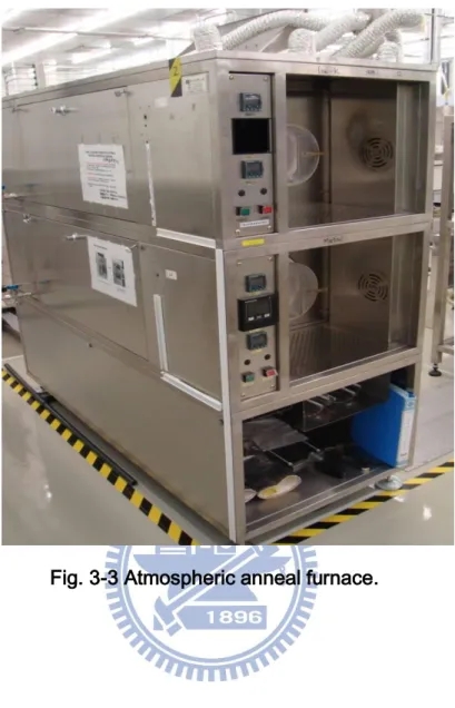
3-3.4 Post Annealing Process
After deposited channel layer and source/drain electrodes, the atmospheric anneal furnace in nitrogen ambience was performed to rearrange the a-ZTO structure. The experimental conditions were controlled at 450 oC
and N2 atmospheric environment. The total annealing time was 1 hr. Figure
30
31
2
Sputtering a-ZTO channel layer3
Sputtering AZO source and drainelectrode
Fig. 3-4 Flowchart of a-ZTO TFTs fabrication.
4
Annealing1
Clean the N++ Si substrate that with thermal oxide SiO2 Gate Si ( N++) SiO2 a-ZTO Gate Si (N++) Gate Si (N++) SiO2 a-ZTO AZO AZO32
3-4. Thin Film Analysis
3-4.1 Measurement of Optical Properties
The transmittance spectrum and optical porperties of the AOSs and TCOs were carried out by the UV-VIS spectrophotometer (Lambda 950). Diagrams of the components of a spectrometer are shown in Figure 3-5. A beam of light from a visible or UV light source is passed through slits, mirrors, and a diffraction grating. The intensity of the reference beam, which is original light source, is defined as I0. The intensity of the sample beam is defined as I. The
transmittance T can be presented as T= and then the other parameters such as absorption coefficient and optical band gap also can be derived.
(a) (b)
Fig. 3-5 (a) UV-VIS spectrophotometer at NCTU and (b) schematics of UV-VIS spectrophotometer.
33
3-4.2 X-Ray Diffraction (XRD)
Bede, D1 High resolution X-ray diffraction (XRD) is mainly for identifying the crystalline phases and determining the orientation as well as the grain size. In XRD, a collimated beam of monochromatic X rays strikes a specimen and is diffracted by crystal planes. By Bragg’s law,
We can calculate the spacing between planes, d, from the wavelength of incident X-ray, λ, and the diffraction angle, 2θ, which is scanned to pick up diffraction from the different crystal planes. By measuring the X-ray profile and further calculation, the orientation of planes of the specimen can be obtained.
In the XRD measurement, the incident angle Omega is 0.5 and scanning 2theta is swept from 20 to 40 .
3-4.3 Surface Morphology
The Digital Instruments Dimension 3100 atomic force microscope (AFM) was used to characterize the step height and roughness. Besides, scanning electron microscopy (SEM) was used to measure the thickness and cross sectional view of thin films. The schematics of AFM and SEM are shown in Figure 3-6.
34
between a probe in AFM and sample surface. By analyzing the two forces, the information of sample surface can be obtained.
In SEM, when the high-energy electrons (10 kV) bombard the sample, the interactions between the electrons and the sample generate the responses. By collecting and analyzing the responses and signals, the surface morphology is obtained.
(a) (b) Fig. 3-6 (a) AFM and (b) SEM in NCTU.
3-4.4 Carrier Concentration and Mobility of Thin Films
The HMS-3000 Hall Effect Measurement System was used to measure majority carrier concentration, carrier mobility, and resistivity of thin film. The Hall effect is the induction of a transverse voltage in a current carrying
35
conductor when the conductor is exposed to a magnetic field that lies perpendicular to current flow. The carrier concentration (n) and the Hall mobility (μH) are related to the induced Hall voltage (VH) by the following
equations:
(3-1)
and
(3-2) where V0 is the voltage across the sample, w the width of the sample, By the applied magnetic field strength, l the length of the sample, d the thickness of the sample, q the carrier charge and Ix the current applied. The schematic of
Hall Measurement System is shown in Figure 3-7.
In Hall measurement, the magnetic field and current were applied with 0.58 T and 50 nA, respectively. The thickness of samples was 50 nm and measured at room temperature.
36
3-4.5 Etching Rate
Etching rate of thin films is determined by the following steps:
1. The 50-nm a-ZTO and a-IGZO films were deposited on glass, respectively.
2. The original transmittance ( ) of a-ZTO and a-IGZO was carried out by the UV-VIS spectrophotometer, and then the transmittances are converted into the absorption coefficient (α) by Beer-Lambert law as shown in Eq. (3-3)
(3-3)
where z is original film thickness
3. The glass with a-ZTO and a-IGZO film was etched by dilute hydrochloric acid (HCl, about 0.39 M) for 1 to 500 seconds, respectively.
4. UV-VIS spectrophotometer was utilized to obtain the transmittance of etched film . The thickness of etched film of a-ZTO/a-IGZO was evaluated by following formula after the and α were obtained.
(3-4)
37
3-5. Device Measurements
3-5.1 Electrical Characteristics
The electrical transfer properties and output characteristics of devices were measured by a semiconductor parameter analyzer (Keithley 4200) in the dark at RT, as shown in Figure 3-8. By applying the voltage on gate and drain, the I-V transistor curves of TFTs were measured. In the output characteristic (IDS-VDS), VDS is conventionally swept from 0 V to 30 V at the step VGS to
measure the corresponding IDS. In the transfer characteristic (IDS-VGS), VGS are
conventional swept from -10 V to 30 V.
Fig. 3-8 Keithley 4200 of NCTU.
3-5.2 Stability Analysis
38
possibly, defect formation in the AOS TFTs, in the gate insulator (GI), or at the active layer/GI interface [34,35]. It might also be expected that an increased temperature or a simultaneous exposure of a device to both bias stressing could lead to enhanced or additional instabilities. In this work, we investigate the electrical stability under 1) positive bias stress (PBS), 2) negative bias stress (NBS), and 3) temperature stress (TBS). The PBS and NBS stressing were applied for 5000 seconds with VGS= 20 V and VGS= -20 V, respectively.
The temperature stressing were applied for 5000 seconds with VGS= 20 V at
80 .
3-6. Summary
The a-ZTO/a-IGZO TFTs with ITO/AZO electrodes were fabricated. The analytic details of a-ZTO/a-IGZO thin film including optical properties, surface morphology, carrier concentration, and etching rate were presented. The performance and stabilities of different TFTs are examined by Keithley 4200 semiconductor analyzer. Also, the measurement conditions were introduced. All of the experimental results and discussions will be summarized in Chapter 4.
39
Chapter 4
Results and Discussions
4-1. Introduction
The thin film performances of a-ZTO and a-IGZO including deposition rate, optical properties, and surface morphology are introduced. The electrical characteristics of a-ZTO/a-IGZO TFTs with ITO/AZO electrodes are compared and discussed. The etching rates of a-ZTO and a-IGZO are analyzed.
4-2. Analysis of Thin Films
4-2.1 Deposition Conditions
Firstly, the deposition rate of a-ZTO is estimated in the beginning of this experiment. Figure 4-1 (a) shows the deposition rate of a-ZTO varies with different sputtering pressures. As the figure depicts, the sputtering rate is linearly decreased with the pressure as it is increased from 3 to 10 mTorr. With the sputtering pressure increases from 3 to 10 mTorr, the deposition rate
40
decreases from 1.87 to 1.14 nm/min. As the chamber pressure is decreased, the mean-free paths of ZnO and SnO2 sputtered atoms become longer and
lead the sputtered atoms to reach the substrate surface more easily. In the reactive sputtering process, the sputtered particles tend to collide with the sputtering gas atoms, which change the transport motion of sputtered particles, causing atoms to arrive at the substrate surface with different kinetic energies. On the other hand, the particles presented in the chamber are proportional to the collisions among sputtered atoms when the sputtering pressure is increased. Therefore, the mean-free path becomes shorter and the efficiency of the deposition rate inevitably reduces. Figure 4-1 (b) shows the deposition rate of a-ZTO varies with different sputtering powers. The increased sputtering power contributes directly to the increment in the number of a-ZTO molecules in the chamber. The deposition rate is also increased with the sputtering power. Thus, the deposition rate of a-ZTO is increased in response to the rise of sputtering power. With the sputtering power is increased from 50 to 80 W, the deposition rate is raised from 1.27 to 3.24 nm/min.
41
(a) (b)
Fig. 4-1 Deposition rate of a-ZTO varied with different sputtering (a) pressure and (b) power.
4-2.2 Optical Properties
To confirm the optical properties of a-ZTO and a-IGZO, the UV-VIS spectrophotometer measurement was performed. The transmittance spectra of a-ZTO and a-IGZO films of 50 nm in thickness are shown in Figure 4-2. The average transmittance in the visible wavelength range (400~700 nm) of a-ZTO and a-IGZO films are 87.25% and 90.53%, respectively. Both a-ZTO and a-IGZO films are in good transparent.
To estimate the energy gap of amorphous thin films, several experimental methods are developed [36,37]. The most common methods are based on absorption coefficient measurements. The energy gap obtained by means of
42
absorption coefficient measurements is known as “optical gap”(Eopt). One
of the standard empirical methods to obtain the optical gap value is the Tauc method, which is proposed by J.Tauc [38]. In this model, a relationship of the optical gap Eopt and absorption coefficient α of thin film is defined according
to Eq 4-1.
(4-1) where the h denotes photon energy, the value of the exponent r denotes the nature of the transition mode including direct and indirect transitions. In the a-ZTO and a-IGZO, r has a value of 1/2 for the direct transition. Above relationship is valid for parabolic conduction and valence bands near the band gap. The Eopt value is obtained by linearly extrapolating the plot of
and finds the intersection with the abscissa. As shown in Figure
4-2, the Eopt values of a-ZTO and a-IGZO are 3.63 eV and 3.66 eV,
respectively. The optical properties of a-ZTO and a-IGZO thin films are summarized in Table 4-1.
43
(a) (b)
Fig. 4-2 (a) Transmittance and (b) Optical band gap of 50-nm thick a-ZTO and a-IGZO film.
Tab. 4-1 Optical properties of a-ZTO and a-IGZO thin film.
Average Transmittance (%) Optical Band Gap (eV)
a-ZTO 87.25 3.63
44
4-2.3 Crystalline Phase and Surface Morphology
The XRD patterns show the crystalline phase of ZTO and IGZO thin films. A 50-nm thick a-ZTO and a-IGZO films were deposited and then annealed in 450 . As shown in Figure 4-3, any sharp ring or spots are not observed, indicating that the films are amorphous.
On the other hand, the surface properties of a-ZTO and a-IGZO films were investigated by AFM and SEM, respectively. The AFM and SEM results are shown in Figures 4-4~4-6. The AFM and SEM images show a clear and uniform surface morphology. There were no grains or grain boundaries due to its amorphous nature. Also, there is no pin hole in both a-ZTO and a-IGZO thin films. It is known that the amorphous films have the advantage of large-area uniformity, low interface state density and low electronic-defect domain [69]. The root-mean-square surface roughness (Rrms) of a-ZTO and a-IGZO was about 0.379 nm and 0.375 nm, respectively. These results indicate that a uniform, amorphous film can be prepared by RF sputtering deposition.
45
(a) (b) Fig. 4-3 XRD results of (a) ZTO and (b) IGZO thin films.
(a)
(b)
(c) Fig. 4-4 (a) Step height of a-ZTO thin film, roughness of (b) a-ZTO and (c) a-IGZO.
46
(a) (b)
Fig. 4-5 3D surface morphology of (a) a-ZTO and (b) a-IGZO.
(a) (b)
Fig. 4-6 SEM results: surface morphology of (a) a-ZTO and (b) a-IGZO thin film.
47
4-2.4 Hall Measurement
The Hall measurement can obtain the thin film qualities including hall mobility, resistivity, and carrier concentration. All the parameters of 50 nm-thick a-ZTO and a-IGZO are summarized in Table 4-2.
Tab. 4-2 Hall measurement of a-ZTO and a-IGZO thin film.
Mobility (cm2/Vs) Resistivity (Ωcm) Carrier concentration (cm-3) a-ZTO 53.7~61.3 4.3~7.9 E2 6 1018~2 1020 a-IGZO 31.7~36.1 2.7~8.5 E2 1016~1018
4-3. Comparisons of a-ZTO and a-IGZO TFTs
4-3.1 Electrical Characteristics of a-ZTO TFTs
The a-ZTO TFTs were deposited at RF power= 80 W, working pressure of 3 mTorr and Ar flow rate=10 sccm; the a-IGZO TFTs were deposited at RF power= 80 W, working pressure = 3 mTorr, gas flow rate of Ar and O2 equal to
10 and 0.6 sccm, respectively. Transfer characteristics of a-ZTO TFTs and a-IGZO TFTs are shown in Figure 4-7. The gate bias swept from -10 V to 30 V.
48
The drain-source voltage (VDS) was set to be 10 V. The channel width (W) and
length (L) of the a-ZTO and a-IGZO TFTs were 1000 μm and 200 μm, respectively. The 40-nm–thick ITO as source and drain electrodes were used in a-ZTO and a-IGZO TFTs. It is observed that the a-ZTO TFTs exhibit Vth of
1.23 V, μFE of 9.29 cm2/Vs, SS of 0.91 V/decade, and Ion/Ioff of 1.46 . In
contrast, Vth, μFE, SS, and Ion/Ioff of a-IGZO TFTs are 1.08 V, 6.73 cm2/Vs, 0.66
V/decade, and 6.53 , respectively. Most of electrical characteristics are similar for these two TFTs. However, the mobility of a-ZTO TFT is even higher than a-IGZO TFT. This improvement is attributed to two major factors: the lower effective mass; and the higher carrier concentration of thin film.
Previous literatures reported the effective mass of a-ZTO and a-IGZO were 0.15 to 0.3 me (me is the rest mass of electron) [39] and 0.34 me [40],
respectively. A simple model gives the approximate relation between effective mass and mobility:
(4-2)
where q is elementary charge, is the carrier effective mass, and is the average scattering time in electric field. This relation indicates that the larger effective mass causes a lower mobility. On the other hand, the carrier concentrations of a-ZTO and a-IGZO are 6 1018~2 1020 [39] and 1016~1018
49
cm-3 [40], respectively. It is reported that the mobility is increased with
increasing carrier concentration and it can be explained by a grain boundary scattering model [32,41]. These results indicate that a-ZTO TFTs show the potential of high mobility TFTs.
Fig. 4-7 Transfer characteristics of a-ZTO and a-IGZO TFTs in saturation region where VDS=10V. a-ZTO a-IGZO Vth (V) 1.23 1.08 μFE (cm2/Vs) 9.29 6.73 SS (V/decade) 0.91 0.66 Ion/Ioff 1.46E7 6.53E6
50
4-3.2 Transfer Characteristics under Positive Bias
Stressing (PBS)
In AMOLED’s, the TFTs are not only used as switches but also as current drivers for pixels. In this case, long-term stability under bias stressing plays a pivotal role for TFTs because a shift of Vth concomitantly leads to a change of
the individual pixel brightness. Therefore, the influence of bias stressing on TFTs must be considered. The transfer characteristics variation of the a-ZTO and a-IGZO TFTs under PBS at RT in the dark box are shown in Figure 4-8. The PBS was stressed at VGS= 20 V and VDS= 20 V up to 5000 seconds. A
positive Vth shift, with little or no change in SS, μFE, and Ion/Ioff was observed.
The Vth, μFE, SS, and Ion/Ioff shift versus stressing time are summarized in
Figure 4-9.
As can be seen in Figure 4-9, Δ Vth is positive. The mechanisms
responsible to the Δ Vth in AOS TFTs are (1) electron trapping in the
channel/gate insulator layer and (2) channel/ambient interactions. The first mechanism means the channel electrons tunnel into the empty trap states in the gate insulator, resulting in the positive shift of Vth. On the other hand, it is
well known that metal oxides are sensitive to molecules in the ambient atmosphere [42,43,44,45]. The bias stressing can lead to field-induced
51
adsorption of O2 and desorption of H2O. Previous researches report that the
oxygen in the environment causes the positive Vth shift under PBS [46,47]. The
adsorbed O2 onto the surface of a metal oxide is an acceptor-like molecule by
following reaction:
(4-3)
The negatively charged oxygen was adsorbed on the channel during the positive gate bias was applied. The buildup of negative space charges easily repelled conduction electrons in channel, resulting in positively shifting of Vth with increasing the duration of PBS.
The measurements of ΔVth for a-ZTO and a-IGZO TFTs have the same
value of 5.45 V. These results indicate both of a-ZTO and a-IGZO TFT have the same stability under PBS.
52
(a) (b)
Fig. 4-8 Transfer characteristics of (a) a-ZTO and (b) a-IGZO TFT in saturation region VDS=10 V under positive bias stressing VDS=VGS=20 V at RT in the dark
box.
Fig. 4-9 Vth, μFE, SS, and Ion/Ioff shift versus stressing time for a-ZTO/a-IGZO
53
4-3.3 Transfer Characteristics under Temperature
Stressing (TBS)
Bias temperature instability (BTI) is recognized as one of the most serious concern in the reliability of TFT technologies [48]. The stabilities of a-ZTO and a-IGZO TFT under high temperature operation were investigated. TBS was stressed at 80℃ with VGS= 20 V and VDS= 20 V for 5000 seconds. The
transfer characteristics variation of the a-ZTO and a-IGZO TFTs under TBS in the dark box are shown in Figure 4-10 and summarized in Figure 4-11. The stabilities are similar between TBS and PBS results, Vth shift positively and
slight change in SS, μFE, and Ion/Ioff. However ΔVth under TBS is larger than
that under PBS and this is due to the thermally activated effect [49]. The stretched-exponential equation for the ΔVth is defined as:
(4-4)
where ΔVth0 is ΔVth at infinite time, represents the characteristic trapping
time of carriers, t is the stressing time, and β is the stretched exponential exponent. is linearly proportional to temperature by the equation of , where T
st is the stress temperature. T0 is related to the energy
parameters of the charge trapping process, although the physical meaning of β0 is not clarified. Therefore, as the stressing temperature increases,
54
increases, resulting in larger ΔVth [50].
The measurements of ΔVth under TBS for a-ZTO and a- IGZO TFTs were
6.79 V and 9.03 V, respectively. Those differences in stability may be due to the impact of ambient effects, defect creation, or electron trapping near interface between the gate insulator and the channel layer. Generally, the major electronic transfer carriers of IGZO and ZTO were oxygen vacancies of In-O and Sn-O, respectively [51,52]. The electronegative of Sn and In were 1.96 and 1.78, respectively, derived from the Pauling scaling. The higher electronegativity in stronger metal oxide bonding results in the dissociation energy of Sn-O (565 kJ/mol) is higher than In-O (318 kJ/mol) [70]. For those reasons, the stronger bonding of Sn-O can reduce the external influences such as channel/ambience effect and electron trapping at gate insulator/channel interface. Consequently, the stability of a-ZTO TFTs is improved compared to a-IGZO TFTs. In summary, compared to a-IGZO TFTs, a-ZTO TFTs exhibits a stable property and hence a-ZTO is a suitable material as the active layer.
55
(a) (b)
Fig. 4-10 Transfer characteristics of (a) a-ZTO and (b) a-IGZO TFT were stressed at 80 with VGS= 20 V and VDS= 20 V.
Fig. 4-11 Vth, μFE, SS, and Ion/Ioff shift versus stressing time for a-ZTO/a-IGZO
56
4-3.4 Transfer Characteristics under Negative Bias
Stressing (NBS)
According to previous study, the most of time that typical TFTs spend under a negative gate bias in AMOLED applications is approximately 500 the amount of time spent under a positive gate bias due to the charging function of AMOLED pixels [53]. The NBS is therefore important as, or even more important than PBS in practical applications. The NBS was stressed at VGS=
-20 V for 5000 seconds. The transfer curves evolution as a function of the NBS time of a-ZTO and a-IGZO TFTs are shown in Figure 4-12 and summarized in Figure 4-13.
As shown in Figure 4-13, that reported a rigid negative Vth shift, with
insignificant changes in μFE, SS, and Ion/Ioff. Previous researches reported that
desorption of H2O in ambience lead to negative Vth shift under NBS [46,54,55].
Desorbed moisture ( ) from the ambience forms positive charged
( ), as depicted following reaction:
(4-5)
where h+ is a hole. The
can act either as electron donor or
acceptor-like traps on the channel layer. The hole concentration is proportional to the NBS duration in the channel layer. The buildups of positive space
57
charges induce electrons easily in the channel layer, resulting in negative shifting Vth under NBS.
The measurements of ΔVth for a-ZTO and a-IGZO TFTs were -1.14 V and
-2.04 V, respectively. These results indicate that both a-ZTO and a-IGZO TFT have the same level of stability under NBS.
(a) (b)
Fig. 4-12 Transfer characteristics of (a) a-ZTO and (b) a-IGZO TFT in saturation region VDS=10 V under negative bias stress VGS= -20 V.
58
Fig. 4-13 Vth, μFE, SS, and Ion/Ioff shift versus stressing time for a-ZTO/a-IGZO
TFTs by a negative bias stress.
4-3.5 Summary of Active Effects
The comparisons of electrical characteristics for a-ZTO and IGZO-based TFTs are presented. Additionally, the stabilities under bias stressing including PBS, PTBS, and NBS are investigated. Table 4-3 summarizes the electrical performance and stabilities in this section. The electrical performance of a-ZTO/a-IGZO TFTs that indicate the mobility of a-ZTO TFT is higher than
59
a-IGZO TFT. This improvement is attributed to two major factors: lower effective mass; and higher carrier concentration of a-ZTO thin film. On the stabilities, the mechanisms of Vth under bias stressing including electron
trapping in the channel/gate insulator, channel/ambient interactions, and thermally activated effect are introduced. The results show that the both of a-ZTO and a-IGZO TFT have the same stability under PBS and NBS, while, compared to a-IGZO TFTs, a-ZTO TFTs improved by 25% of ΔVth under TBS.
In contrast to a-IGZO TFTs, a-ZTO TFTs presented higher mobility and better stability, illustrating that a-ZTO is a suitable material for the active layer of AOS TFTs.
60
Tab. 4-3 Comparisons of electrical performances of a-ZTO and a-IGZO TFTs.
4-4 Comparisons of a-ZTO TFTs with ITO and AZO
Electrodes
4-4.1 Electrical Characteristics of a-ZTO TFTs with In-Free
Electrodes
To date, the industrial standard of transparent conducting oxide (TCO) is tin-doped indium oxide or ITO. However, to achieve In-free TFTs, ZnO based TCOs such as AZO as the alternative electrodes are fabricated and studied.
a-ZTO TFTs a-IGZO TFTs Vth (V) 1.23 1.08 SS (V/decade) 0.91 0.66 μFE (cm2/Vs) 9.29 6.73 Ion/Ioff 1.46 E7 6.53 E6 PBS: Vth (V) 5.45 5.45 TBS: Vth (V) 6.79 9.03 NBS: Vth (V) -1.14 -2.04
61
Comparisons between ITO and In-free TCO of AZO as source and drain electrodes in a-ZTO TFTs were studied.
The 40nm-thick ITO electrodes were deposited at RF power= 50 W, working pressure of 3 mTorr and Ar flow rate=10 sccm, while the 40 nm-thick AZO electrodes were deposited at 80 W, 3 mTorr, gas flow rate of Ar and O2
equal to 10 and 0.5 sccm, respectively. The average transmittance in the visible wavelength range of AZO and ITO films are 93.3% and 89.9%, as shown in Figure 4-14. The result demonstrates AZO and ITO films have the good transparent property. The electrical transfer characteristics of a-ZTO TFTs with ITO and AZO as source and drain electrodes are shown in Figure 4-15. It is observed that the a-ZTO TFTs with AZO electrodes exhibit Vth of
1.46 V, μFE of 1.96 cm2/Vs, and SS of 0.86 V/decade. In contrast, Vth, μFE, and
SS of a-ZTO TFTs with ITO electrodes were 1.23 V, 9.29 cm2/Vs, and 0.91 V/decade, respectively. The results indicated that a-ZTO TFTs with ITO electrodes exhibited μFE of 9.29 cm2/Vs, which is almost a factor of 5 higher in
the mobility and higher on-current (Ion) than that of a-ZTO TFTs with AZO
electrodes. This is due to the ITO has lower resistivity than AZO.The resistivity of ITO and AZO measured by four point probe are and
![Fig. 1-3 Cross section structure diagram of the TFT-LCD panel [23].](https://thumb-ap.123doks.com/thumbv2/9libinfo/8739461.203954/23.892.175.794.268.710/fig-cross-section-structure-diagram-tft-lcd-panel.webp)
![Fig. 1-5 Photographs of (a) 6.5 inch flexible full-color top emission AMOLED panel with a-IGZO TFTs as back plane [25] and (b) 32 inch prototype OLED TV driven by a-IGZO TFTs [26]](https://thumb-ap.123doks.com/thumbv2/9libinfo/8739461.203954/25.892.169.741.111.372/photographs-flexible-emission-amoled-plane-prototype-oled-driven.webp)