國 立 交 通 大 學
光電工程學系博士班
博士論文
主動陣列觸控面板與光感測器之畫素電路研究
Study on the Pixel Circuits of Active Matrix
Touch Panel and Light Sensor
研 究 生:周祿盛
指導教授:戴亞翔 博士
主動陣列觸控面板與光感測器之畫素電路研究
Study on the Pixel Circuits of Active Matrix Touch Panel and
Light Sensor
研 究 生:周祿盛 Student: Lu-Sheng Chou
指導教授:戴亞翔 博士 Advisor: Dr. Ya-Hsiang Tai
國 立 交 通 大 學
光電工程學系博士班
博士論文
A Dissertation
Submitted to Institute of Electro-Optical Engineering,
Department of Photonics, College of Electrical and Computer Engineering, National Chiao Tung University
in Partial Fulfillment of the Requirements for the Degree of
Doctor of Philosophy in
Electro-Optical Engineering July 2013
Hsinchu, Taiwan, Republic of China
主動式陣列觸控面板與光感測器
之畫素電路研究
研究生:周祿盛 指導教授:戴亞翔博士
國立交通大學
光電工程學系
摘要
本論文研究如何利用薄膜電晶體元件特性來開發整合觸控面板或光感測器 於平面顯示器之相關課題,在元件研究的基礎下,考慮感測器或感測電路在實際 情況下所會面臨的問題並提出改善方法。 在觸控感測部分,我們利用了原先在顯示器中造成設計困難的 RC 時間延遲 原理,設計出新型觸控感測電路。此利用前後條掃描線所驅動的觸控感測畫素電 路上,當人體觸控造成電容值增加時,將使得前後掃描線訊號的開電壓脈衝出現 重疊的情況,在此重疊期間,感測電路將會導通並輸出一電晶體開電流等級之感 測訊號。故此電路相較於其他主動式觸控感測電路具有大訊號易讀取的優點,對 於後端讀取系統的需求度較低,可有效降低整體產品之成本。同時開關電流的訊 號比也提供了感測電路對於元件變異性的高容忍度。而當感測電路未被讀取或觸 摸時,感測訊號僅為電晶體的關電流等級,此低電流輸出可有效降低整個感測面 板之功耗,達到節能的效果。本文詳盡討論各種可能利用 RC 時間延遲概念製成 的觸控電路組成,並且嘗試以非晶矽與非晶矽銦鎵鋅氧化物之薄膜電晶體製作此 感測電路,以證明此種感測電路技術可適用於不同材料之電晶體製程中。此外,所提出之感測電路技術亦可適用於內嵌式或外貼式二種結構。對應不同的結構, 電路之設計亦有所不同,為此我們提出該感測電路設計的流程,以利於此感測電 路技術更快速且有效地應用於平面顯示器中。除了利用此技術製作之 2 吋觸控面 板實際驗證電路功能以外,本文並進一步以模擬方式討論此技術應用於大尺寸觸 控感測面板之可行性與可能面臨到的問題,結果顯示即使是 42 吋的大型面板, 此技術仍可使用。 在光感測應用上,我們分別討論了背光與正光感測應用。傳統非晶矽薄膜電 晶體對於背光照射時,受下閘極遮蔽而無光電流反應,且正光照射時只有在元件 關區域產生 nA 等級的小電流信號,我們認為它並不適合作為感測元件。此文中 我們引進另一種結構,稱為間隙型非晶矽薄膜電晶體。此電路為非對稱結構,在 下閘極與汲/源極之一端有一可透光之區域,此區域可作為感光區,使得此種元 件在照光時有較明顯的光電流反應。同時此元件可在開區域中具有光效應,較大 的感測電流可增加感測電路之訊雜比。文中詳細討論此種元件的光敏感度,找出 最適當的操作方式來設計背光與正光感測電路。接著分析在實際應用中可能會造 成誤差的因子,包含:元件均勻性、溫度效應、與照光可靠度分析,尤其非晶矽 材料對於長時間照光有嚴重的光電流衰退現象,稱為 Staebler-Wronski (SW)效 應,若無法校正此效應之影響,則非晶矽材料將很難使用於光感測應用中。文中 我們分別針對間隙型非晶矽薄膜電晶體在照光下的電流劣化行為,並提出校正方 法與可整合於平面顯示器中的光感測電路。 利用所提出的觸控與光感測畫素電路技術,可使顯示面板多功能化,省去外 部元件,以更輕薄化及低成本的方式,來實現具高畫質及互動功能的智慧型顯示 器。
Study on the Pixel Circuits of Active Matrix
Touch Panel and Light Sensor
Student: Lu-Sheng Chou Advisor: Dr. Ya-Hsiang Tai
Department of Photonics & Institute of Electro-optical Engineering,
College of Electrical and Computer Engineering
National Chiao Tung University
Abstract
This dissertation studies the issues about how to develop touch panel or light sensor integrated in flat panel displays using thin film transistors. The possible problems in the practical applications of the sensors and the sensing circuits are discussed and their respect solutions are proposed.
For the touch sensing, the principle of RC time delay on the scan bus, which makes the display design difficult, is applied to invent the new touch sensing circuit. A pair of consecutive scan buses is used to drive the proposed touch sensing circuit. When human touch causes the capacitance increase, the turn-on pulses of the scan bus signals overlap. In this overlapping time, the proposed circuit outputs an ON-level current as a sensing signal when it is touched. Compared to other touch sensing technologies, the touch signal of the proposed circuit is obvious and easy to be read out. Therefore, the cost of the readout IC can be reduced. Meanwhile, the large signal provides the immunity against the device variation. On the other hand, if the pixel is not activated or touched, the output current is at the OFF-level, which can save the power consumption. In this study, the different circuit configurations using RC delay
are discussed. The circuits are further implemented by amorphous silicon (a-Si) and a-IGZO TFTs to prove that the proposed circuit is universal to different kinds of TFTs. Furthermore, the circuit can be adapted in both structures of out-cell and in-cell. For the various conditions of using the circuit, we propose a general design procedure, which can be helpful to apply the circuit in flat panel displays more quickly and effectively. In addition to the demonstration of a 2 inch touch panel to check the validity of the circuit function, we further discuss the feasibility and possible issues in applying the proposed method to large panels by simulation. The results show that the circuit is applicable even for the 42-inch panel.
In the aspect of the light sensing, we respectively discuss the sensing for the backlight and the front light. The conventional a-Si TFT has little photo response to backlight illumination because the blockage of the metal gate, and it only has photo response in the nA order in the OFF region under front illumination. We think it is not suitable to be a photo sensor. In this study, we introduce an a-Si TFT with asymmetric structure, called gap-type a-Si TFT, which has a gap as a sensing region between bottom gate and one of the source and drain electrodes. The gap-type TFTs have obvious photo sensitivity in ON region not only under backlight illumination but under front illumination. The large sensing current can improve the signal-to-noise ratio. The photo sensitivity of the gap-type TFTs are examined to look for the best operation condition. After that, we analyze the error factors for the sensing in real cases, including device uniformity, temperature effect, and reliability under illumination. Especially, the a-Si suffers from a serious current degradation under continuing illumination, which is well known as Staebler-Wronski effect. If the influence of the effect cannot be offset, it will be difficult to use a-Si for light sensing. In this study, we analyze the current degradation behavior of the gap-type a-Si TFT under illumination. The calibration method and the light sensing circuits integrated in
flat panel display are proposed.
Using the proposed touch sensing and light sensing pixel circuits, a flat display can be embedded with multiple functions with no need of extra devices. In this way, the panel can be made in a thinner form and lower cost. A smart display with good image quality and interactive function can thus be implemented.
誌 謝
還記得剛考完研究所後回到外婆家,外婆問了我:「祿盛阿,你會不會一直 念到博士阿?」當時心想,哪有可能!豈知北上找完教授後,回家便告訴家人我 打算攻讀博士。似乎在研究所生涯的開頭,就預告了未來將有著與過往完全不同 的思維與訓練。 在完成博士學位的過程中接受了許多人的幫助,最感謝的莫過於我的指導教 授戴亞翔老師。感謝老師給予我許多的協助,無論是學術上的研究與心態上的調 整及分享,不斷的鼓勵讓我可以慢慢累積養分藉以成長茁壯;更重要的是當我在 研究所生涯後半期遭遇到各種困難時,體諒我並給予無數支援,讓我有足夠的能 量克服過程中的難題,也給了未來人生不同的啟發。 此外要感謝的老師也包含了同在顯示所的田仲豪老師、冉曉雯老師與劉柏村 老師。感謝田老師與冉老師除了學業知識的教授外,在申請博班逕讀時願意給予 推薦。此外常從劉老師這邊得到實驗上與其他事務上的協助,也謝謝劉老師願意 成為我的口試委員,與其他口試委員包括柯明道教授、張鼎張教授、林志隆教授、 陳科宏教授與許鉦宗教授,對於我的研究內容給予許多寶貴的意見。對於同是口 試委員的張鼎張教授於研究過程中慷慨的提供我們研究過程中許多資源,讓我的 研究可以順利進行,在此也致上我至高的敬意。 承蒙眾多學長姐、同學與學弟妹的幫助,除了研究上有所進展外,也讓我在 實驗室的生活可以多采多姿。感謝小黑、首席、國珮、紹文、騰瑞、歐趴的引導讓我可以很快進入研究生生活。也謝謝贊文、立峯、光揚、家揚學長在行政與論 文投稿上的協助。還有同實驗室同甘共苦的夥伴,趴趴、少宏,及大學就當同學 一直到博班的耿維,感謝你一路上的幫忙與支持,感謝皓麟、俊文、士哲、彥甫 學長給予資源上的協助與學術經驗上的指導。同屆中劉老師實驗室的 Dolly、光 廷、俊傑、敬儒與李老師實驗室的品佐、又瑋,有你們這些同學的扶持我才能一 路走到現在! 除此之外,也要感謝實驗室學弟幫忙完成許多研究上的成果。謝謝寬達與政 哲幫忙完整的研究觸控技術開發與驗證;冠銘、柏成、嘉鴻協助設計 OLED 補償 電路;政達、詠暄幫忙 X-ray 感測電路分析討論並協助建立相關量測機台;謝謝 君毅在我最後準備論文期間協助處理許多事,讓我可以專心並順利完成論文口 試。當然還需感謝其他實驗室學弟妹的幫忙,如品睿、揚順在實驗上也提供我及 實驗室所需之幫助。當然受到的幫助遠遠超過在這上面所寫的人,雖無法一一提 及答謝,然所受之恩惠銘感於心。 當然不能忘了我的家人還有我的女友詩敏,感謝你們全心全力的支持我,讓 我可以無後顧之憂的完成我的學業,追逐人生的夢想,你們對我的恩惠榮耀了 我,也讓家人的關係變得更加緊密,謝謝你們!最後,我想將這論文獻給我的外 婆,雖然你來不及看到我的畢業,但你將永存我的心中,希望往後我的表現可以 令你感到驕傲! 祿盛 2013 夏 於風城新竹
Contents
Abstract (Chinese)
………. iAbstract (English) ………iii
Acknowledgments ……….vi
Contents ……….viii
Figure Captions ………x
Tables Captions ……….…xvi
Chapter 1 Introduction to Interactive Sensing Technology
1.1 General Background ---011.2 Review and Motivation --- 04
1.3 Thesis Organization --- 04
Chapter 2 Touch Sensing
2.1 Introduction ---122.2 Scan Pulse Distortion and Overlapping---13
2.3 Sensing Circuit Evolution ---13
2.4 Circuit Discussion and Demonstration ---17
2.5 Large Panel Simulation --- 19
2.6 Summary ---22
Chapter 3 Backlight Sensing
3.1 Introduction---473.2 Device Property---48
3.3 Error Analysis---50
3.4 Backlight Sensing in Flat Panel Display--- 55
Chapter 4 Front-light Sensing
4.1 Introduction--- 83
4.2 Device Property--- 84
4.3 Error Analysis---86
4.4 Front Light Sensing in Flat Panel Display--- 90
4.5 Summary---91
Chapter 5 Conclusion and Future Work
---112References
--- 114Vita
--- 120Figure Captions
Chapter 1
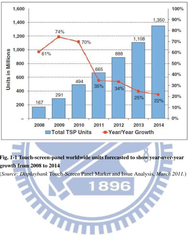
Fig. 1-1 Touch-screen-panel worldwide units forecasted to show year-over-year growth from 2008 to 2014 ………7 Fig. 1-2 The diagram of the TSP industry ………..….8 Fig. 1-3 The structure categorization of TSP, which also indicates the difference between the out-cell (embedded) and in-cell (integrated) type TSP ……….9 Fig. 1-4 The sensing work on Microsoft Kinect ………...10 Fig. 1-5 The figure of this dissertation structure ………...11
Chapter 2
Fig. 2-1 DisplaySearch divides touch into ten categories with 14 sub-technologies ………..23 Fig. 2-2 The original scan signal of display at scan near end ………24 Fig. 2-3 The original scan signal of display at scan far end ………..24 Fig. 2-4 The 2T1R1C sensing circuit using two single-gate IGZO TFT…………...25 Fig. 2-5 The sensing result of the 2T1R1C pixel circuit ………...26 Fig. 2-6 The first touch sensing pixel circuit using dual-gate IGZO TFT …………27 Fig. 2-7 (a) The cross-section (b) the symbol of the dual-gate IGZO TFT ………..28 Fig. 2-8 The transfer characteristics of the dual gate TFT ………29 Fig. 2-9 Id–VBG transfer characteristics of the dual gate TFT under five different
Fig. 2-10 The transfer characteristics of the dual gate IGZO TFT (a) sweeping VTG =
VBG (b) VTG = -10V, sweeping VBG and (c) VBG = -10V, sweeping VTG.
………...31 Fig. 2-11 The sensing result of the first touch sensing pixel circuit using a dual-gate IGZO TFT ………...32 Fig. 2-12 The 1T1R1C sensing pixel circuit using a single-gate IGZO TFT ……….33 Fig. 2-13 The sensing result of the 1T1R1C pixel circuit ………...34 Fig. 2-14 The sensing results of (a) the 2T1R1C (b) the 1T1R1C pixel circuit using single-gate a-Si TFT ………...35 Fig. 2-15 The verification of the threshold voltage shift of the TFT. (a) Pixel 1 and pixel 2 illustrate touch and untouched cases, respectively. (b) The simulation result indicates that the proposed circuit is able to distinguish the sensing difference even when the threshold voltage shift of the TFT is 5V. ………..36 Fig. 2-16 The (a) 3T1C (b) 2T1C touch sensing circuit in which the transistor with a fixed gate bias replaces the resistor component in the RC low-pass filter…38 Fig. 2-17 A demonstration of the 2 inch touch panel ………..39 Fig. 2-18 Flow chart of design procedure ………...40 Fig. 2-19 (a) the locations of four corners in the panel (b) Four corners simulation result of the designed 42 inch touch panel using the proposed 2T1C circuit……42 Fig. 2-20 3T1C circuit without voltage drop on the scan bus for the simulation of multi-touch situation ………...43 Fig. 2-21 2T1C circuit with voltage drop on the scan bus for the simulation of multi-touch situation ………...44 Fig. 2-22 (a) Simulation result of pulse high of multi-touch situation with 3T1C circuit
(b) Simulation result of pulse high of multi-touch situation with 2T1C circuit ………..45 Fig. 2-23 Four corners simulation result of 2T1C circuit when pulse high decrease...46
Chapter 3
Fig. 3-1 Schematic of local dimming function by LED backlight ………58 Fig. 3-2 (a) Cross-section and (b) Transfer characteristics of the conventional a-Si TFT ……….59 Fig. 3-3 Transfer characteristics of the gap-type a-Si TFT with (a) gate-near-drain mode and (b) gate-near-source mode ……….….60 Fig. 3-4 Drain current versus backlight illumination intensity (a) in OFF region (b) in ON region ………...61 Fig. 3-5 (a) The normalized drain current versus backlight illumination intensity of ON region and ON region (b) The relative photosensitivity of ON region and OFF region ………...62 Fig. 3-6 Transfer curves of the gap-type TFT with different gap lengths (a) i=5um (b)
i=12um (c) i=30um ……….63 Fig. 3-7 (a) Schemes of gap-type TFTs with different open-ratio (b) The relation between ID_illum and open_ratio ………...……65
Fig. 3-8 The drain current versus illumination intensity curves of 8 devices and (b) Error analysis of ON current variation between the measured light intensity and the illuminated light intensity ………..66 Fig. 3-9 The drain current versus illumination intensity at Vgs=9, 10, 11 V and (b) Error analysis of the threshold voltage shift between the measured light intensity and the illuminated light intensity ………67 Fig. 3-10 The drain current versus illumination intensity at T= 35, 40, 45 °C and (b) Error analysis of temperature variation between the measured light intensity and the illuminated light intensity ………..68
Fig. 3-11 The drain current versus temperature at Vgs= 10V, Vds= 10V and (b) The
TC versus temperature curves of 4 devices ………69
Fig. 3-12 The measured current of a-Si TFT under optical stress ………...70
Fig. 3-13 The relation between ID_illum and open_ratio after optical stress ………….71
Fig. 3-14 The ID/Open-ratio versus open-ratio (a) before (b) after optical stress…...72
Fig. 3-15 (a) Calibration of SW effect and (b) error analysis with/without calibration ………..73
Fig. 3-16 The different stress intensities, the curves present two different degradation rates ……….74
Fig. 3-17 (a) Calibration of SW effect and (b) error analysis under two-step stress intensities ………75
Fig. 3-18 Proposed 4T2C light sensing circuit and (b) The time diagram ………….76
Fig. 3-19 ID-VD curve for photo current simulation ………..77
Fig. 3-20 Simulation results of light sensing circuit ………...79
Fig. 3-21 (a) Equivalent circuit and (b) layout of the proposed sensor………80
Fig. 3-22 A backlight sensing unit in panel ……….81
Fig. 3-23 Schematic diagram of sensor array embedded in panel ………..82
Chapter 4
Fig. 4-1 The linearity between the illuminance and the photocurrent of lateral PIN photodiodes with area= 1000/11000/121000 μm2 ………..93Fig. 4-2 The cross-section of (a) the conventional a-Si TFT (b) the gap-type a-Si TFT ……….94
Fig. 4-3 The transfer curves of the conventional a-Si TFT with the front light illumination ……….95 Fig. 4-4 The transfer curves of the front illuminated gap-type a-Si TFT operated in (a)
gate-near-drain mode (b) gate-near-source mode ………...96 Fig. 4-5 The relationships between photocurrent and illumination intensity of
gap-type TFTs for several bias conditions in (a) the ON region and (b) the OFF region ………..97 Fig. 4-6 The normalized drain current versus front light illumination intensity of ON and OFF region (b) The relative photosensitivity of ON region and OFF region ………..98 Fig. 4-7 (a) ON current variations of a-Si TFTs of 4 devices (b) Error analysis of ON
current variation between the measured and the illuminated light intensities ………..99 Fig. 4-8 (a) The ON current versus illumination intensity at 35°C, 40°C, and 45°C (b)
Error analysis of temperature variation between the measured and the illuminated light intensity ……….100 Fig. 4-9 (a) The ON current versus temperature at Vgs=10V, Vds=10V (b) The
temperature coefficient versus temperature curves of 4 devices (c) Error analysis of temperature variation between the measured and the illuminated light intensity ………101 Fig. 4-10 Schematic diagram of the real situation of the a-Si TFT in panel………..103 Fig. 4-11 (a) The ON current versus front light illumination intensity without backlight and with backlight (b) The relationship between the measured and the illuminated light intensity in ON region (c) Error analysis of backlight effect between the measured and the illuminated light intensity in ON region ………104 Fig. 4-12 The behavior of gap-gate a-Si:H TFTs under the stress of 16673 lux front
Fig. 4-13 Behavior of gap–gate a-Si:H TFTs under the stress of 19160 lux back light ………107 Fig. 4-14 Drain currents measured with and without backlight illumination after front light stress ……….108 Fig. 4-15 Ratio R with respect to front illumination under front light of 13600 lux for different stress time ……….………..109 Fig. 4-16 (a) Measured intensity back traced by parameter R. (b) The error comparison of with and without calibration under different stress time of 13600 lux front light ……….110 Fig. 4-17 The proposed front light sensing array circuit using gap-gate TFT……...111 Fig. 4-18 The timing scheme of the proposed circuit ………...111
Table Captions
Chapter 2
Table 2-1 The specification of the designed 42 inch touch panel ………41
Chapter 3
Table 3-1 I0(L) and R0= 1/A0(L) at VGS= 10V with the illumination intensity variation
………..78 Table 3-2 Circuit simulated conditions ………78
Chapter 1
Introduction
1.1
General Background
The development of the twisted nematic (TN) [1] and supertwisted nematic (STN) [2] cell configurations, along with the necessary manufacturing technologies [3~6], resulted in the birth of the LCD industry in the late 1970s and early 1980s. The subsequent development of thin-film transistor (TFT) technology provided a further boost to the industry in the late 1980s [7~8]. The boom was significantly supported by the advancement of material technologies such as the highly reliable manufacturing of liquid crystal base materials, and the development of polymers for the alignment layer, color filter materials, and sheet-type polarizers formed from the poly(vinyl alcohol)-iodine complex [9].
Following the notebook application, in the late 1990s, the TFT LCD is gradually replaced the dominance of the cathode-ray tube (CRT) monitor in TV market [9~10]. At the beginning of the development, the TFT LCD was pursued for the improving in image quality and providing more image information in unit area. The resolution of TFT LCD is required as high as possible. Soon it had not been the only goal since the resolution is corresponding to the need for human vision. Therefore, the manufacturers aimed to scale the TFT LCD up, which can provide more image information on a TFT LCD. After overcoming some problems, such as off-axis image quality, moving picture quality, and reasonable manufacturing yields, the large-area TFT LCD can be fabricated with lower price and gradually erodes the lead of the plasma display panels even in very-large-area display application. However, fostering
the large-area LCD panel should face some questions. The first, the manufacturer needs to build new factory of next generation for large-size glass substrate, which critically raises the investment including the factory building, clean room, and other process facilities. Second, the large LCD panels also raise the technique difficulties in the peripheral equipment or process issues. Besides, building the factory for large-size LCD panels can lower the cost on unit area of panels and increase the competition for market share, but the low product price could be the reason of the deficit if the demand of display panels is insufficient [10]. Furthermore, as the viewpoint of the panel resolution, the display size should be confined by the human vision and other factors such like user space and the environment conditions.
In order to reduce the risk in slack and increase the demand for panels, the TFT LCD is going to the way that integrates sensing technologies and provides more functions for applications. Owing to the participation of sensing technologies, the position of display has been more important and almost necessary for people life, which becomes a main interface to receive the information and response the control signals of user. In addition, the lifetime of the conventional products is often determined by the malfunction of the conventional button for frequent usage. The integration of the sensing technology can effectively solve the problems and grant them the possibility of amazing applications. At present, the touch sensing and the light sensing technologies are prevalent to be applied in TFT LCD especially in mobile devices.
In 2007, Apple Corporation announced the first smart phone which supports the multi-touch function and starts an evolution of mobile phones. After that, touch screen panels (TSPs) have been widely used in other electronic products such like tablet PC, LCD monitor, portable player, etc [11~12]. Fig. 1-1 illustrates the annual growing of TSPs. To meet the rapid and abundant requirement, as shown in Fig. 1-2, an industry
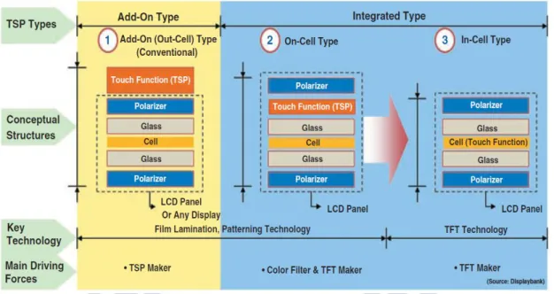
has formed to provide the needed component, driver, or module of TSPs. For the aspect of the structure, TSPs can be mainly categorized into out-cell, on-cell, and in-cell types, as shown in Fig. 1-3. To compare the TSP of different structures, the additional component adhered on the display panel for sensing touch events reduces the contract ratio and brightness [13]. For the aspects of light weight, good display quality, and reducing production cost for touch screen, the in-cell TSPs have much potential to substitute for the out-cell TSPs since the touch sensing circuit of the in-cell TSPs can be integrated into display panel [13~14]. However, the out-cell TSP still dominates in current touch-sensing application due to the lower technique difficulty and higher stability.
The light sensing has been used in TFT LCD for many years. Many applications were studied and revealed including image scanner, fingerprint scanner, and active pixel sensors [15~16]. Recently, light sensing in display is used as an interactive input for 3-dimension touch sensing, which further extends the applied domain of display. In 2006, another light sensing application on console game device for body motion detection was proposed by Nintendo Corporation, Japan. The sensor embedded in the remote controller can detect the infrared to locate the coordinates and then simulate the hand feature and motion. Starting from the proposal, the body motion detection technology is generally applied to the gaming market. Fig. 1-4 illustrates another motion detection using IR detection proposed by Microsoft. However, as can be seen in Fig. 1-4, the detection method needs the additional component. If we can use the TFT as the light sensing device, the light sensor can be integrated into TFT panel so that the product can be simplified and reduces the fabrication cost.
The combination of touch sensing and light sensing technology makes TFT LCD have flexibility and possibility for more interactions between people and products. Even though many researches of them including some commercial products have been revealed individually, there is no effective method to combine the two technologies into an active matrix panel yet. Based on the in-cell TSPs concept, TFT LCD is a potential candidate to integrate the two sensing technology. Besides, in order to extend the application domain, the target should be aimed at the large size interactive display not only at the mobile electronics, which would raise the integration difficulty especially for TSPs.
In this thesis, we would examine the role of TFTs in the two sensing technologies and solve the possible issues when the panel integrates the sensing circuits. For example, if used as a light sensing device, the amorphous silicon (a-Si) TFT suffers serious current degradation under continuous illumination, i.e. Staebler-Wronski (SW) effect. Another case is that the device variation affects the sensing result of the active touch sensing circuit. The device characteristics of the TFTs would be analyzed in the respect of the applications in touch and light sensing. After that, the corresponding circuits would be properly designed and integrated into TFT LCD.
1.3
Thesis Organization
There are five chapters in this dissertation, in which can be summarized in Fig. 1-5. The general background of TFT LCD industry is introduced in chapter 1, which also introduces the applications of touch and light sensing in TFT LCD. In chapter 2, we propose the active touch sensing circuit and design a 42-inch touch panel using our proposal. After that, the light sensing is categorized into backlight sensing and front-light sensing and discussed in chapter 3 and chapter 4, respectively. In the two
chapters, the SW effect under backlight and front light illuminations are studied to find the calibration methods for practical application. Finally, the summarization of all experimental results in this dissertation and the suggestions for the future work are presented in chapter 5. The structure is in the other way listed below for indexing:
Chapter 1 Introduction to Interactive Sensing Technology
1.1 General Background 1.2 Review and Motivation 1.3 Thesis Organization
Chapter 2 Touch Sensing
2.1 Introduction
2.2 Scan Pulse Distortion and Overlapping 2.3 Sensing Circuit Evolution
2.4 Circuit Discussion and Demonstration 2.5 Large Panel Simulation
2.6 Summary
Chapter 3 Backlight Sensing
3.1 Introduction 3.2 Device Property 3.3 Error Analysis
3.4 Backlight Sensing in Flat Panel Display 3.5 Summary
Chapter 4 Front-light Sensing
4.1 Introduction 4.2 Device Property 4.3 Error Analysis
4.4 Front Light Sensing in Flat Panel Display 4.5 Summary
Fig. 1-1 Touch-screen-panel worldwide units forecasted to show year-over-year growth from 2008 to 2014
Fig. 1-2 The diagram of the TSP industry
Fig. 1-3 The structure categorization of TSP, which also indicates the difference between the out-cell (embedded) and in-cell (integrated) type TSP
Chapter 2
Touch Sensing
2.1
Introduction
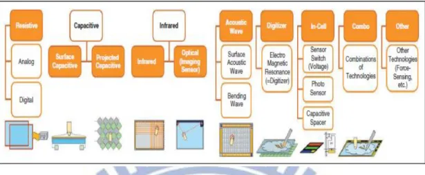
In addition to the structure difference, as shown in Fig. 2-1 [17], TSPs have various sensing methods mainly including resistive [14,18~20], capacitive [13,21~26], and optical sensing [27~29]. The same type TSP in both of in-cell and on-cell structure faces some identical problems. Photo detection touch sensors have been revealed to be sensitive to the ambient light, which easily causes sensing noise, since they determine the touch signal using the light reflection or absorption. For resistive touch sensors, although they have the advantage of low cost, the poor reliability lowers their potential for the application in high-valued productions. Comparing to the two types touch sensors, the capacitive touch sensors are dominant in most high-valued products benefiting from the merits of high reliability, high sensitivity, and easiness for multi-touch sensing. However, they suffer some problems for large size touch panels. The touch signal of the capacitive sensor is determined by the output current difference between touch and untouched event [25~26]. The signal gets distorted by the parasitic resistance and capacitance on the signal bus in a large size panel, which makes the readout ability of the external circuit become more critical for large area application.
Moreover, in addition to above identical problems, the in-cell TSPs using thin film transistors have extra issues as following description. Firstly, in order to increase the open ratio, source follower is usually adapted to buffer the voltage signal to the read out bus. Nevertheless, as a unity-gain buffer, the source follower cannot amplify
a small voltage signal. Second, because of the threshold voltage difference between the input and output of a source follower, a sensing error can be arisen from the threshold voltage variation of thin film transistor (TFT) devices. Furthermore, whether pixels are touched or not, the source followers consume power to put out the sensed voltages, which power should be further reduced.
In this work, we want to discuss a novel active touch sensing circuit, which can be implemented in on-cell and in-cell structure. Meanwhile, it can effectively overcome the above mentioned issues for large-area in-cell TSPs.
2.2
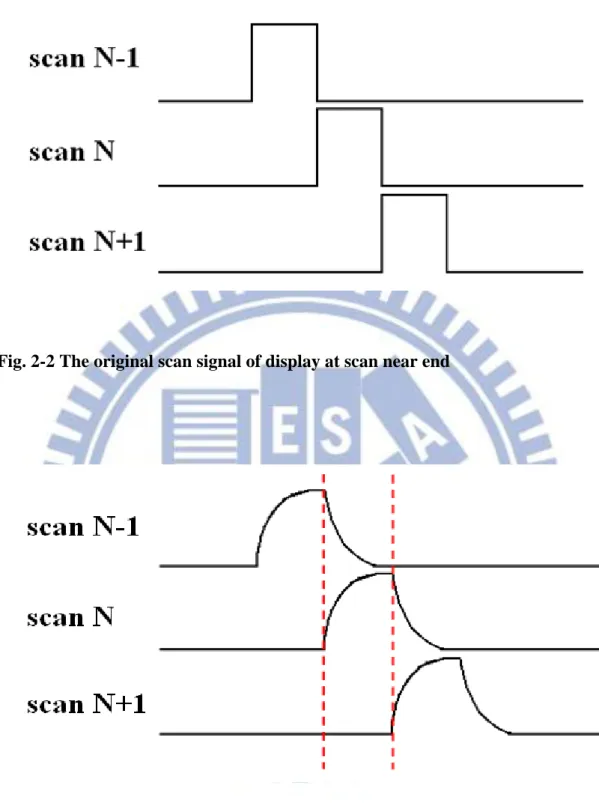
Scan Pulse Distortion and Overlapping
In display, the original scan signal is given as a pulse, which is shown in Fig. 2-2. When the Nth scan pulse turns off, the (N+1)th scan pulse becomes turn-on
immediately. As we know, there are some parasitic resistances and capacitances on the scan line. When a scan pulse propagates on the scan line, it gets distorted by the parasitic resistances and capacitances, so that the pulse at scan far end has delay with a RC time constant, and its shape is shown in Fig. 2-3. In Fig. 2-3, we can see that as the Nth scan pulse not completely turning off, the (N+1)th scan pulse starts to turn on.
It causes there a temporary pulse overlapping which keeps TFT turned on when the new data comes on to the shared data bus. It causes the error of the pixel voltage and it is not what we want to see in display. On the contrary, in the proposed touch sensing circuit, we intentionally use the TFT ON current which is induced by pulse overlapping to detect whether pixel is touched or not.
2.3
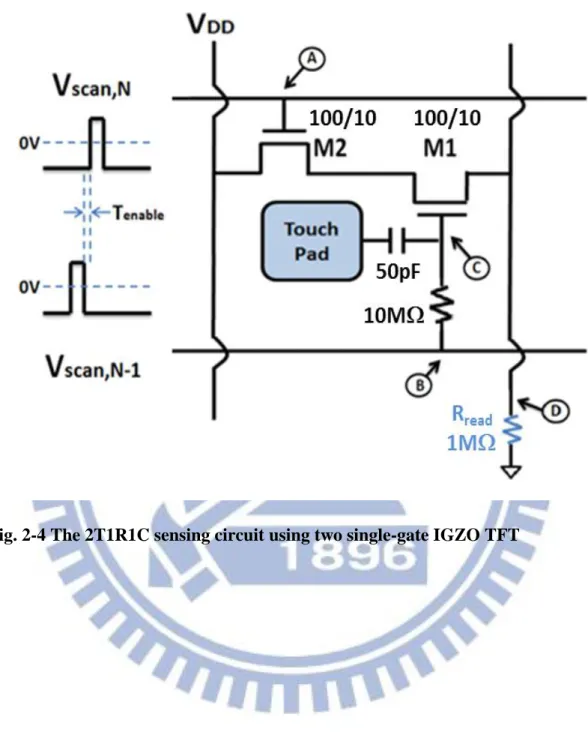
Sensing Circuit Evolution
Fig. 2-4 shows the sensing circuit which composed of two single-gate TFTs connected in series, one resistance R, and one sensing capacitance Csen. We feed two consecutive scan pulses N-1 and N at node B and A, respectively. When sensing pad is untouched, the pulse at node C is almost the same as that at node B, and the two TFTs are not in ON state at the same time. In such a case, there is no current occurs when pixel is untouched. On the other hand, when sensing pad is touched by human’s hand, the pulse at node C is seriously distorted by the resistance R and sensing capacitance Csen. The distorted pulse at node C overlaps with the pulse at node A temporarily. The pulse overlapping when sensing pad is touched causes both TFTs turn ON concurrently. Therefore, when pixel is touched, there is a significant ON current, which can be a judgment for whether pixel is touched or not.
Fig. 2-5 shows the schematic of the sensing circuit with the input signals and its measurement result. In laboratory-level experiment, the RC low-pass filter is connected by discrete components including a capacitor of 50 pF and a resistor of 10 Mohm, and a readout resistor of 1 Mohm is used to transfer the current to voltage signal for the oscilloscope measurement. For the touched case, VA is high and VC is
not low enough to turn off the TFT. The spikes in the output voltage waveform (Vout)
on the readout resistor indicate the touch events. In other words, when touch event occurs, it results in a significant transient current. On the other hand, for the untouched case, no current is observed. It implies that the proposed sensing method does not consume readout power when sensing circuit is not touched.
2.3.2 1T1R1C Using Dual-Gate IGZO TFT
A similar sensing circuit using a dual-gate IGZO TFT can be used to replace the two single-gate TFTs, as shown in Fig. 2-6. It comprises a dual-gate IGZO TFT, a resistor R, and a sensing capacitor Csen. The top and the bottom gates of the TFT are
connected to the two successive scan pulses, respectively. The difference is that the scan pulse is fed to the top gate by way of an RC low-pass filter.
The process flow of the dual-gate a-IGZO TFTs is described as following. Shaped Ti/Al/Ti gate electrodes were capped with SiNx gate dielectric which was deposited by plasma enhanced chemical vapor deposition (PECVD). For the S/D metal, Ti/Al/Ti was formed by successive deposition with DC sputtering at room temperature. By patterning and dry etching these layers, the S/D electrode was formed. After that, the active layer of 30-nm-thick a-IGZO film was deposited by DC magnetron sputtering system using a target of In:Ga:Zn = 1:1:1 and defined after etching. Finally, devices were capped by the passivation at 280℃, and then ITO were patterned for top gate. The device cross-section and the symbol of a dual-gate TFT are shown in Fig. 2-7.
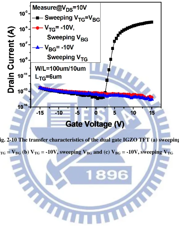
From previous references, the electrical characteristics of dual-gate IGZO TFT are greatly improved with respect to the conventional single-gate IGZO TFT, which is shown in Fig. 2-8 [30~31]. In addition, we also investigated the I–V characteristics of the dual-gate IGZO TFT with different bias voltages applied to each gate. Fig.2-9 shows the transfer curves of drain current (Id) versus bottom-gate voltage (VBG) for
the dual-gate IGZO TFT at different top-gate voltages (VTG). These transfer curves
exhibit parallel shifts with respect to different VTG values. This phenomenon is
attributed to attraction and expelling of free carriers in the active layer by the top-gate. As illustrated in Fig. 2-10, the TFT is kept OFF by biasing VTG at -10V even when the
VBG is as high as +10V, and vice versa. It implies that, the threshold voltage of the
dual gate IGZO TFT using the bottom-gate in its normal operation can be controlled by the top-gate and vice versa.
The following explains the operation of pulse overlapping method in more detail. For most of the time, both the top and bottom gates of the dual-gate TFT are set
at -10V, and the TFT is turned off. Just before the VBG pulse coming to the bottom
gate, the pulse of VTG is sent to the top gate through the RC circuit. If no touch event
occurs at this time, the RC time delay is small. Thus, the slightly distorted VTG pulse
can fall in time to -10V to turn off the TFT before the VBG comes in. On the other
hand, if a touch event happens, it results in large RC time delay. The larger RC delay leads to more serious pulse distortion and prolongs the voltage falling time of VTG.
This delay time keeps the TFT from turning off by the time that the bottom-gate switches to +10V. In such a case, a significant transient ON current flows through the TFT to be the sensing signal. Consequently, we can use the method to detect touch events. Fig.2-11 shows the laboratory-level test result.
2.3.3 1T1R1C pixel circuit
Another 1T1R1C pixel circuit using conventional single-gate TFT and its laboratory-level test are shown in Fig. 2-12 and Fig. 2-13, respectively. Comparing to the previously proposed circuit, it further omits a vertical bus of VDD from the pixel,
which make the new circuit more suitable for the in-cell touch sensing. The simple circuit can decrease the consumption of aperture ratio and increase the transmission.
In operation, when the panel is untouched, the scan pulse Vscan,N-1 is firstly fed to
node B and raise the voltage of node B, VB , to 10V. At this time, the TFT does not
output current because there is no voltage difference between drain and source. Then, although the scan pulse Vscan,N comes in and raises the voltage of node A, VA, to make
a voltage difference between drain and source, the VB has fallen in time to -10V to
turn off the TFT. On the other hand, if touch event increases the sensing capacitance, which consequently increases RC time-constant, the scan pulse Vscan,N-1 gets a
distortion when it reaches the gate of TFT. Therefore, it needs more time to lower the voltage from 10V to -10V. When the scan pulse Vscan,N rapidly raises from -10V to10V,
a transient ON current is produced by the pulse overlapping.
For a good design, the transient ON current should occur only when the selected sensing pixel circuit is touched. To avoid false current, we introduce a time interval, Tenable, between two consecutive gate pulses, which ensure VB can get back to
-10V before VA starts rising. Tenable avoids the intrinsic distortion owing to the
parasitic RC influence on row bus in the large area active matrix. It is noteworthy that the distortion on VC without touch is resulted from the parasitic capacitance and
resistance of the transistor. The parasitic capacitance and resistance emphasize the importance of Tenable.
As can be seen in the circuit schemes, the proposed circuit is mainly operated by the scan pulses. The operation of the scan pulses is identical to that in display driving even the use of Tenable. In general display scan driving, Tenable is used to ensure that the
Clc cannot be influenced by the data voltage of the next pixel. Therefore, the display and touch sensing scan pulses should be able to be provided by the same scan driver. In practical signal process, each data line could be connected to a charge integrator and biased by the integrator [25].
2.4
Circuit Discussion and Demonstration
2.4.1 Circuit Advantages
One of the values of the proposal is universal to the backplane structure, including on-cell and in-cell. Although the design results are different, the effective circuit and the design procedures are the same. For example, the obvious difference for the two structures is the sensing capacitor fabrication. In the on-cell structure, the touch sensing array can be fabricated individually and then attached to the display panel. In this case, the sensing capacitor can be formed by the cover glass sandwiched
in between finger and the electrode fabricated in the touch sensing array and protected by the cover glass. On the other hand, in the in-cell structure, the capacitor in this RC circuit can be the liquid crystal capacitance (Clc), which is formed by the electrodes made on the TFT substrate and the common electrode on the color filter substrate. The Clc can be increased by the external forcing to compress the gap of the two electrodes [25~26]. However, although the capacitor fabrications are different, the capacitance can be proper calculated and simulated. Furthermore, the proposed sensing circuit is also suitable to different TFT types, such as amorphous silicon (a-Si) TFT, oxide TFT, and poly-silicon (LTPS) TFT. In addition to the previous test using IGZO TFT, Fig. 2-14 shows the test results of 2T1R1C and 1T1R1C sensing circuit using a-Si TFT. For our test devices, since the Vth controlled ability of the top gate of dual-gate a-Si TFT is not so obvious like dual-gate IGZO TFT, no test result of the sensing circuit using dual-gate a-Si TFT is included in this dissertation.
The in-cell types of touch panel which detects the change in the liquid crystal capacitance [25~26] usually have two disadvantages. One is that, the amplifying TFT outputs large current even in the case without touch and thus keep consuming power whether pixels are touched or not. The other issue is the threshold voltage shift of TFT. In a sensing array, different sensing pixels on the vertical line share the same readout circuit. Because of the threshold voltage variation of the TFTs in different sensing pixels, touch signal and untouched signal in different pixels could be harder to distinguish by the same readout circuit. Although the uniformity of a-Si TFT is excellent, the device variation of other type TFTs including LTPS or oxide TFT could affect the circuit performance. In addition, the threshold voltage of TFT would shift under electrical stress of usage.
The proposed circuit only output current when the selected pixel is touched so that the power consumption could be reduced. Furthermore, the effect of threshold
voltage variation on the proposed circuit can be avoided, as shown by the simulation result in Fig. 2-15. We use the same a-Si TFTs size and charge integrator to perform the simulation. As can be seen in Fig. 2-15(b), there still is a 0.4V difference between touched signal and untouched signal when threshold voltage shifts 5V in one pixel but -5V in another pixel. In our design, the output signal is more dependent on the overlapping time of the pulses than the threshold voltage of the TFT. This provides the big tolerance of the threshold voltage variation.
2.4.2 Demonstration Using a-Si TFT
In the demonstration, a transistor with a proper fixed gate bias, namely, RTFT is
used to replace the resistor. The alternative pixel circuit is shown in Fig. 2-16. Besides, the voltage bias for RTFT in every sensing pixel is fixed, so it can be provided by Vcom.
By doing this, it is practical in fabrication to save more aperture area than implementing the resistor with a long metal wire. Fig. 2-17 shows a demonstration of the proposed circuit using a-Si TFT in a 2-inch 9x9 array.
2.5 Large Panel Simulation
In this section, we design a 42 inch a-Si active touch panel using the proposed
circuit and discuss the problems arisen from the large size.
2.5.1 Design Consideration, Procedure, and Results
There are many factors to design the large-area panel of the proposed sensing method, such as bus line width, size of TFTs, and sensing capacitance. For example, to make the sensing area becomes larger, the scan line width can be made thinner but it will cause a large parasitic resistance on the scan line and thus a serious RC time constant delay. The delayed scan pulse at scan far end might result in a false touch signal. When this case happened, the same readout setting cannot be applied at both
scan near and far ends. On the contrary, if the scan line width is designed to be wide, it squeezes the area of sensing region. In such a case, the small sensing area corresponding to the small sensing capacitance may not make large difference in the RC time constant between the cases of touched and untouched. Another example is the size of RTFT and the driving TFT. Increase in the driving TFT size can improve the
ability to charge the data bus and the read out circuit, while the gate capacitance of TFT increases accordingly. Therefore, the difference of total capacitance at sensing node when pixel is touched or untouched is less significant, and the intrinsic RC time constant delay of scan pulse increases.
Due to these intertwined design factors, a design procedure is proposed to support our task, as shown in Fig. 2-18. It contains the following steps:
Step1: Specify panel size, aspect ratio, and resolution Step2: Design line width of scan and data line
Step3: Calculate the area of sensing region, which value is the area of one pixel pitch subtracting the area of bus line and TFTs of one pixel. For a fast estimation, the area of TFTs is ignored because it is much smaller than the area of bus line. The value of sensing capacitance can be calculated accordingly.
Step4: Design sizes of both driving TFT and RTFT.
Step5: Calculate the parasitic capacitances and resistances on the buses. Step 6: Verify the design with SPICE simulation.
The design procedure is repeated until the design passes the criteria concerning the significant voltage difference between touch and untouched. In this paper, the target of our design is to produce a voltage difference larger than 0.2V, which is good enough for a common voltage comparator in the peripheral readout circuit to judge the touch event. Table 1 lists our final design results.
2.5.2 Four-Corner Simulation
Since the large touch panel suffers from serious parasitic capacitance and resistance on the scan and data buses, the intrinsic RC delay of these buses can possibly make the sensing pixel fail. Therefore, the simulations were conducted for the four pixels of the four corners of the designed 42 inch touch panel. The simulation results shown in Fig. 2-19 include the scan pulses and the output signals of the four pixels when they are touched and untouched. The output signal of the pixel at the scan far end is larger than that at the near end owing to the intrinsic bus delay. The output signal from the pixel at data near end is larger than that from the data far end, because the current signal from the data far end has to pass through the parasitic resistances and capacitances of the data bus, while the current from the pixel at the data near end comes out directly. For the worst cases, the smallest touched signal appears at scan near end and data far end, and the largest untouched signal appears at scan far end and data near end. The worst-case difference is shown by the two dash lines of the output signal in Fig. 2-19. This difference between the touched and untouched signals is still larger than our design target of 0.2V.
2.5.3 Current-Induced Voltage Drop on Scan Bus
There is yet another concern of the proposed circuit that when many pixels on the same scan line are touched simultaneously, every touched pixel drains current from the scan bus. This is not an issue for the 2T1R1C pixel circuit and the 1T1R1C using the dual-gate TFT since the sensing current comes from the individual voltage bias buses in column. For 1T1R1C using single-gate TFT, the total sensing current drained from the same scan bus in row flowing through resistances of scan bus results in the voltage decrease of the scan pulse. In this case, we need to confirm the circuit can still function when the heavy load of multi-touch happens.
The pixel circuits of 3T1C and 2T1C shown in Fig. 2-20 and Fig. 2-21, respectively, were simulated for the two cases without and with the voltage drop on the scan bus. For the both circuits in a row of 10 and with all the pixels touched simultaneously, the simulation results of the scan pulse high voltage are shown in Fig. 2-22(a) and 2-22(b), accordingly. It can be observed that there is more decrease of scan pulse high voltage in 2T1C circuit than in 3T1C circuit. However, the decrease is as small as 0.22V.
We simulate the worse situation that when the scan pulse high voltage decreases from 10V to 7V, which corresponds to hundreds of pixels on the same scan line are touched simultaneously. The result is shown in Fig. 2-23. It can be seen that the minimum touched signal is still larger than the maximum untouched signal for 0.2V, which still meets the design target. The concern of voltage drop owing to multi-touch on the scan bus for the large area panel can be relieved.
2.6 Summaries
A simple but novel concept of pulse overlapping detection for the active matrix touch panel is proposed. The proposed circuit has many advantages. Firstly, the output signal of the transient on current of TFTs is significant and thus can be easily readout by low cost ICs. Secondly, current signal only occurs when a pixel is touched. The power consumption in operation is greatly reduced. Moreover, device variation can be tolerated, which is the major advantage over the other active touch panels of the source follower type. A 42 inch touch panel of the proposed method is successfully designed by the proposed design procedure. The proposed circuit can provide an excellent way of implementing large area active matrix touch panels.
Fig. 2-1 DisplaySearch divides touch into ten categories with 14 sub-technologies
Fig. 2-2 The original scan signal of display at scan near end
(a)
(b)
Fig. 2-8 The transfer characteristics of the dual gate TFT.
Fig. 2-9 Id–VBG transfer characteristics of the dual gate TFT under five different
Fig. 2-10 The transfer characteristics of the dual gate IGZO TFT (a) sweeping VTG = VBG (b) VTG = -10V, sweeping VBG and (c) VBG = -10V, sweeping VTG.
Fig. 2-11 The sensing result of the first touch sensing pixel circuit using a dual-gate IGZO TFT
(a)
(b)
Fig. 2-14 The sensing results of (a) the 2T1R1C (b) the 1T1R1C pixel circuit using single-gate a-Si TFT
Figure 2-15(b)
Fig. 2-15 The verification of the threshold voltage shift of the TFT. (a) Pixel 1 and pixel 2 illustrate touch and untouched cases, respectively. (b) The simulation result indicates that the proposed circuit is able to distinguish the sensing difference even when the threshold voltage shift of the TFT is 5V.
(a)
(b)
Fig. 2-16 The (a) 3T1C (b) 2T1C touch sensing circuit in which the transistor with a fixed gate bias replaces the resistor component in the RC low-pass filter.
(a)
(b)
Fig. 2-19 (a) the locations of four corners in the panel (b) Four corners simulation result of the designed 42 inch touch panel using the proposed 2T1C circuit
Fig. 2-20 3T1C circuit without voltage drop on the scan bus for the simulation of multi-touch situation
Fig. 2-21 2T1C circuit with voltage drop on the scan bus for the simulation of multi-touch situation
(a)
(b)
Fig. 2-22 (a) Simulation result of pulse high of multi-touch situation with 3T1C circuit (b) Simulation result of pulse high of multi-touch situation with 2T1C circuit
Chapter 3
Backlight Sensing in Flat Panel Display
3.1
Introduction
For LCD-based products, 90% power consumption is attributed to backlight [32]; accordingly, backlight power saving is considered one of the most effective ways to reduce LCD energy dissipation. In recent years, the light-emitting diode (LED) backlighting is sought to replace the fluorescent backlighting because of the advantages including ultra wide color gamut, increased contrast through local dimming, improvement in motion picture response time by scanning, lower power consumption, and elimination of mercury [33~37]. However, the LED backlight modules could be non-uniform in large panel or degrade after a long time operation [38], which directly influences the image quality and limits the competitiveness of LED backlight in large-size flat display panels.
In this chapter, we propose the backlight sensor for the accurate backlight intensity. The degraded LED backlight can be corrected by the feedback of the backlight sensor [39], so the lifetime of display can be prolonged. Moreover, the using of backlight sensors can enhance the performance of backlight-control technologies. For example, the local dimming technology means that it can adjust the backlight intensity according to the frame which would be showed. Fig. 3-1 is the schematic of backlight local dimming. The backlight sensors can be used to detect the light intensity and determine the intensity whether or not to achieve the value that it should be.
3.2
Device Property
Before proposing the sensing circuit, we should fully study the photo response of sensing devices. Fig. 3-2(a) and Fig. 3-2(b) show the cross-sections and the transfer characteristics of the illuminated conventional a-Si TFT, respectively. We find that the conventional TFT does not have any photo reaction. This phenomenon is easy to figure out from the inserted diagram in Fig. 3-2(b). The bottom gate metal blocks all the possible backlight which would illuminate on active layer. Therefore, the conventional TFT does not be considered to be our backlight sensing device.
To reduce the effect of gate metal shielding, a non-conventional structure is proposed as the sensing device. Comparing to the conventional a-Si TFT, the non-conventional structure TFT has a gap which exists between bottom gate and one of top metal electrodes (source or drain). We define the gap size as i and call this structure TFT as “gap-type TFT” [40]. Since it has the same fabrication process as the conventional a-Si:H TFT, the light sensor can be integrated in panel without changing the mask number and extra cost. The basic process flow is described as following. After the deposition and patterning of gate metal on the glass substrates, three layers, i.e., silicon nitride (SiNx, 3500 Å ), a-Si:H, and n+ a-Si:H films, were successively deposited in a plasma enhanced chemical vapor deposition (PECVD) system. After source/drain electrodes were made, the n+ a-Si:H region with length (L) of 5 μm between the source/drain electrodes was etched off by a reactive ion etch. Then, a passivation layer was used to cap the channel region.
The transfer characteristics of gap-type TFTs (i=30um) are showed in Fig. 3-3. Since the gap-type TFT is asymmetric, it can be alternatively operated. Fig.3-3(a) is the gate-near-drain mode, and Fig. 3-3(b) is the gate-near-source mode. For further discussion, we define the ratio of the TFT drain current under illumination ( ID_illum )
to that in the dark ( ID_dark ) as RL/D = ID_illum / ID_dark [41]. We can find that the RL/D of
the gate-near-source one is larger not only in OFF region ( Vgs = -10V ) but also in ON region ( Vgs = 10V ). In aspect of application, the gate-near-source one has better photosensitivity to be the sensing device. From Fig. 3-3(b), the RL/D can achieve to 4
orders both in OFF region and ON region.
Since the operating region of sensing device should be properly in sensing circuit, we examine the device performance in different operation regions. Fig. 3-4 shows the OFF current and ON current versus the backlight intensity. They cannot be compared directly because of the different current levels. To analyze the photosensitivity in detail, we normalized the curves of Fig. 3-4 (a) (b) and show the results in Fig. 3-5(a). Next, we differentiate the normalized current to the illumination intensity. The relative photosensitivity versus illumination intensity is showed in Fig. 3-5(b). There is an intersection point at about 10000 lux. It means that the sensing device operated in ON region has better photosensitivity under 10000 lux illumination. On the contrary, the device operated in OFF region has better photosensitivity above 10000 lux. On the basis of the following reasons, we decided to operate the sensing device in ON region to sensing backlight. In TFT-LCD, backlight must pass through the polarizer and then achieve the TFT array layer. The actual backlight intensity illuminate on the TFT array would not over 10000 lux. Another reason for choosing ON region is that the ON current is higher about 2 orders than OFF current, which can reduce the effect of noise and be read easily.
The non-conventional TFT can detect the backlight because the gap exists. Fig. 3-6 shows the transfer characteristics of the gate-near-source TFT with different gap sizes ( i = 5um、12um、30um ). When the gap increases, the photosensitivity will be higher in ON region. Theoretically, we should use the gap as large as possible for
great photosensitivity of the backlight sensing, but it will reduce the pixel aperture ratio. Besides, for the TFTs of the various gap lengths, the different dark current levels lead us to hardly analyze and apply to sensing circuit. To reduce the variables, we use the gap size i = 30um to be the experimental devices.
For further understanding of the relation between the gap and the photo effect, we design different structures of gate-near-source TFT, as shown in Fig. 3-7(a). It can be seen that there are two gates in the new devices, and the length between original bottom gate and the drain is still 30 um. The function of the extra gate is to shield the backlight illumination. The extra gate does not be given any bias, in other words, it is floating. The new devices are benefit to control the photo response without dark current change. We define “Open-ratio” to name the new structures. For example, the original structure which gap can be illuminated entirely then we call it open-100%. If the area of gap is shielded 67% from backlight illumination by floating gate, then we call it open-33%. Fig. 3-7(b) shows that ID_illum is proportional to the open-ratio. It
means that the photo effect is proportional to the illuminated area of the gap.
3.3
Error Analysis
After realizing the device properties, some factors caused error on sensing TFTs are considered in this section.
3.3.1 Device Uniformity
3.3.1.1 ON Current Variation
The measured ON currents of eight devices with respect to the illumination intensity are shown in Fig. 3-8(a). Four of them are on sample-A glass substrate and the other four are from another glass substrate sample-B. We average the eight measured currents, and take it as the reference. Then, the originally measured current
is looked up the illumination intensity according to the reference. This corresponding backlight intensity is called Luxmeasured. Since it is different from the device really
shined, the light intensity (Luxreal), the error can be defined as “
real real measured Lux Lux Lux ”. Fig. 3-8(b) shows the error from the on current variation of the eight devices. It has a maximum error 7.5% at 5400 lux illumination.
3.3.1.2Threshold Voltage Shift
For the effect on Vth shift, we simulate it by changing Vgs level. Fig. 3-9(a) shows the ID at Vgs=9V, 10V, and 11V, which represents the influence of Vth shift ±1V in the case of Vgs=10V. We find that there has little change owing to Vth shift. It can be understood from the insert diagram in Fig. 3-9(a). The diagram shows the
ID_illum is almost independent of the gate voltage in ON region. Similarly, we take
the Vgs=10V as a reference, and then calculate error of the cases of the Vgs=9V and Vgs=11V corresponding to the backlight intensity. From the result of Fig. 3-9(b), the maximum error is only 3.28%, which shows that the threshold voltage shift will not cause too much influence to light sensing.
3.3.2 Temperature
In application, the sensor is embedded in TFT array, and the panel’s internal temperature will change during usage. Thus, we need to consider the temperature effect of device. Assume 40℃ is the panel’s normal operating temperature, and it is subject to ±5℃ variation. Fig. 3-10(a) shows the measured current of device-1 at 35 ℃、40℃ and 45℃. Calculating the error of four devices, we find the maximum error can be up to 16.4%, which cannot be neglected and needs to be reduced.
Fig. 3-11(a) shows the curves of the photo drain current versus temperature. With the temperature increasing, the drain current also raises gradually [42]. We fit
these curves linearly and define the slopes as a temperature coefficient (TC). Under different illumination intensities, we can get the different TCs. It means that the device does not have the identical response to temperature under different illumination intensities. Fig. 3-11(b) further shows the relation between TC and illumination intensity for four devices. We find there is an obvious variation of temperature response from device to device. This phenomenon will make it more difficult to develop a calibration method. Therefore, for reducing the error caused by temperature variation, we propose to control the temperature of the panel instead of calibrating it. When the temperature variation is controlled within ±3.5℃, and the error can be reduced to 10%.
3.3.3 Device Reliability
3.3.3.1 Staebler-Wronski (SW) effect
Several possible sensing error factors like device uniformity, temperature, and instability of a-Si must be considered. However, from the study of photo current response of a-Si:H TFTs, Staebler-Wronski (SW) effect is a dominant influence to light sensing [43~45]. The predominant explanation of the effect is that the illumination leads to the creation of additional meta-stable states in the band gap of the amorphous silicon, by breaking the weak bounds of the hydrogen atoms to the silicon, which decreases the lifetime of excess carriers and thus reduces the photoconductivity.
To study the SW effect, we use 19160 lux backlight to illuminate the device,
and the stress time is from 0 sec to 4800 sec. Fig. 3-12 shows the result of optical stress. It can be observed that the current degrades obviously with stress time increasing. In addition, the exposure time of the measurements (15 sec.) is much less than light stress time (600 ~4800 sec). Hence, we neglect the degradation resulted