國 立 交 通 大 學
電子工程學系 電子研究所碩士班
碩 士 論 文
使用變壓器回授及正向基底偏壓壓控振盪器之
研究
The study of using transformer feedback voltage
control oscillator with forward body bias
研 究 生:陳冠翰
指導教授:荊鳳德 教授
使用變壓器回授及正向基底偏壓壓控振盪器之
研究
The study of using transformer feedback voltage
control oscillator with forward body bias
研 究 生:陳冠翰 Student: Kuan-Han Chen
指導教授:荊鳳德 博士 Advisor: Dr. Albert Chin
國立交通大學
電機學院 電子與光電學程
碩士論文
A Thesis
Submitted to College of Electrical and Computer Engineering National Chiao Tung University
in partial Fulfillment of the Requirements for the Degree of
Master of Science in
Electronics and Electro-Optical Engineering June 2007
Hsinchu, Taiwan, Republic of China
使用變壓器回授及正向基底偏壓壓控振盪器研究
學生 : 陳冠翰 指導教授 : 荊鳳德 教授
國立交通大學
電子工程學系 電子研究所碩士班
摘要 本論文描述如何設計一個低電壓、低功率損耗及低相位雜訊的金氧半壓控振盪 器。討論如何利用變壓器回授來增強電晶體的轉導以達到降低功率同時又拉大輸 出擺幅的效果。使用基底偏壓後,又進一步的改善整個架構。此差動振盪器使用 TSMC 0.18um CMOS 製程並經由 ADS momentum 做 EM 模擬分析。在此設計一個操作10GHz 的壓控振盪器,約有 9.5GHz 頻率調整範圍,在振盪頻率距 1MHz
The study of using transformer feedback voltage control
oscillator with forward body bias
Student: Kuan-Han Chen Advisor: Prof. Albert Chin
Department of Electronics Engineering & Institute of Electronics
National Chiao-Tung University
Abstraction
Design of low-voltage, low-power CMOS Voltage-Controlled Oscillator(VCO) will be investigate in this thesis. We will discuss how to use transformer feedback to enhance transconductance to reduce power consumption and achieve high output swing at the same time. After using forward body bias, we improve the structure further. The differential VCO is implemented using TSMC 0.18um process. The EM simulation results with ADS momentum. A designed 10GHz VCO achieves a turning range of 9.5GHz, and phase noise about -112dBc at 1MHz offset frequency with power consumption 1.3 mW.
誌 謝
感謝我的指導教授-荊鳳德教授,給予我的論文指導和鼓勵,讓我
在電路設計這一方面得以有更進步的空間。讓我在這一段兩年的時間
學習到許多作學問的態度與方法。
同時也感謝實驗室學長-張慈學長及在長庚大學任教的瑄苓學
姐,對我在研究與量測上,提供你們寶貴的經驗與知識給我,給我很
多幫助。與思麟學長的切磋討論,更是激發了許多靈感的火花,理論
的辨證。
還有一起奮鬥的順芳、柏翔、和鉅宗,大家一起研究討論,和學
弟、學長一起打球、出遊,都是我碩士生活中美好的回憶。還要感謝
NDL的汶德跟書毓以及交大的熙良,給了我許多知識與量測上的幫
助,使得我能更進一步了解到各種細節的重要。
還要感謝我的父母給我的栽培與期望,讓我在做研究時,生活沒
有後顧之憂,使我能順利完成學業。
最後希望各位實驗室的學長、弟、妹,都能順順利利地作好自己
的研究,願祝各位前程似錦,一帆風順。
陳冠翰
98 年 6 月
Contents
Abstract (in Chinese)...I
Abstract (in English)...II
Acknowledgements...III
Content...IV
Figure captions...VI
Table Lists...VIII
CHAPTER 1
INTRODUCTION...1
1.1 Introduction... 1
1.2 Technology concept...2
1.3 Motivation...3
CHAPTER 2 OSCILLATOR THEORY...4
2.1 General concept...5
2.2 Parameter issue...7
2.2.1 Quality factor...7
2.2.2 Tuning range and K
VCOof Oscillators...8
2.3 Varactor...9
2.3.1 Diode Varactor...9
2.3.2 MOSFET Varactor...10
2.3.3 AM-FM Conversion...12
2.4 Inductor...13
2.4.1 Inductor...13
2.4.2 Transformer...15
2.5 Phase noise...19
2.5.1 Noise Source...20
2.5.2 Lesson’s Model...21
2.5.3 Linearity and Time Variation...22
CHAPTER 3 CMOS LC TANK OSCILLATOR THEORY...26
3.1 Negative-R oscillator ...26
3.2 Differential LC-tank voltage-controlled oscillator...28
3.3
Phase Noise Operation in Differential LC-Tank Voltage
Controlled Oscillators.. ...31
3.4 Transformer Feedback Voltage Controlled Oscillator...34
3.4.1 Drain-Source Transformer Feedback VCO...35
3.4.2 Drain-Gate Transformer Feedback VCO...36
3.4.3 Back-Gate Transformer Feedback VCO...37
CHAPTER 4 SIMLATION AND MEASUREMENT...39
4.1 Proposed design...39
4.2 Simulation...43
4.3 Measurement...45
CHAPTER 5 VCO DESIGN FLOW...48
5.1 Design procedure...48
CHAPTER 6 CONCLUSIONS and IMPROVEMENT...49
6.1 Conclusions...49
6.2 Improvement...51
References...52
FIGURE CAPTIONS
Figure 1.1 RF transceiver structure -1-
Figure 2.1
Basic feedback oscillator model -5-
Figure 2.2 Feedback system with frequency-selective network -5-
Fig 2.3 (a) oscillator structure (b) one-port view of (a) -6-
Fig 2.4 Definition of bandwidth in Q factor -7-
Fig 2.5 Principle of switched tuning method -8-
Fig 2.6 Reversed-Biased PN Junction -9-
Fig 2.7 Nonlinear C-V characteristic -10-
Fig 2.8 Accumulation mode MOS varactor -10-
Fig 2.9 Typical oscillation waveform of MOS varactor , ref [6] -11-
Fig 2.10 Spiral Inductor -13-
Fig 2.11 Simple equivalent model of Spiral Inductor -14-
Fig 2.12 (a) Transformer layout (b) Schematic symbol ref. [8] -15-
Fig 2.13 (a) Low frequency model (b) High frequency model -16-
Fig 2.14 (a) Two asymmetrical inductor(b) a symmetrical inductor
-17-
Fig 2.15 (a) Lump-circuit model (b) single-ended (c) differential
excitation -18-
Fig 2.16 (a) Spectrum of ideal Oscillator (b) Spectrum of actual
Oscillator
-19-Fig 2.17 (a)
fa > fb(b)
fa < fb-22-
Fig 2.18 (a) maximum voltage response (b)zero crossing response
-23-Fig 2.19 Conversion of noise to phase fluctuations and phase noise
sidebands, ref [11] -24-
Fig 3.1 Equivalent Model -26-
Fig 3.2 (a) Negative-Gm Oscillator (b) small-signal model -26-
Fig 3.3 (a) voltage control frequency (b) f-V relationship -27-
Fig 3.4 (a) differential VCO (b) differential VCO with tail current-28-
Fig 3.5 Nonideal LC tank model -29-
Fig 3.6 (a) No current source (b) Ideal noiseless current source -32-
Fig 3.7 noise filter with (a) capacitor alone (b) Complete noise filter
-33-
Fig 3.8 the transformer-based CMOS VCO
-34-Fig 3.9 (a) Drain-Source Feedback VCO (b) Voltage Waveform -35-
Fig 3.10 (a) Drain-Gate TF-VCO (b) Complementary VCO with
Drain-Gate Transformer Feedback -36-
Fig 3.11 Back-Gate Transformer Feedback VCO -37-
Fig 3.12 the simulation of proposed VCO compared with different
topologies.
-37-Fig 4.1 (a) Add body bias on NMOS (b) Add body bias on NMOS
with transformer feedback -40-
Fig 4.2 simulation of Gm vs. VGS -40-
Fig 4.3 Proposed Circuits -41-
Fig 4.4 Four port broadside couple transformer -42-
Fig 4.6 Phase noise -43-
Fig 4.7 Tuning Range -44-
Fig 4.8 Spectrum -45-
Fig 4.9 Tuning Range -45-
Fig 4.10 Phase noise -46-
Fig 4.11 Layout -47-
Fig 4.12 Microphotograph -47-
Fig 5.1 (a) DNW inductor (b)
Patterned Ground Shields inductor -51-
Table Lists
Table 3.1 Comparisons of VCO structure in Fig 3.4 -31-
Table 4.1 transconductance comparison -41-
Table 4.2 Q comparison of transformer -42-
Table 4.3 Specification -46-
Chapter1
1.1Introduction
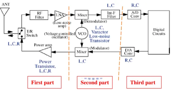
In the last few years, many advanced research and development has been made in area of wireless communication technology. Such as mobile phone, wireless mouse, wireless local area network (WLAN), global positioning satellite (GPS), RFID tags, Bluetooth etc. Those applications have become an important role in our life. In general, radio-frequency model plays two parts of functions in communication system.
Fig 1.1 RF transceiver structure
First part was designed to receive and transmit signal. Second part which did modulation and de-modulation called IF frequency system. This part combined with phase locked loop(PLL) and frequency synthesizer was implemented by analog / digital circuit (mixed-mode circuit). The last part deals with the transformation of analog signal and digital signal. The process called baseband system.
The radio-frequency model combined the first part and second part. The system with receiver and transmitter called transceiver. It included low noise amplifier (LNA), mixer, voltage controlled oscillator (VCO), and power amplifier (PA). This research
is focus on the design of VCO.
1.2 Technology concept
Pseudomorphic High Electronic Mobility Transistor (pHEMT) FET, Hetero-junction bipolar transistor (HBT), bipolar junction transistor (BJT), CMOS, Bi CMOS, LDMOS are common implementation of RF integrated circuit.
Each implementation technology has their advantage and drawback, so it is the reason why individual implementation component built systems are favored for so many years. CMOS for base band section, bipolar for IF partition, ceramic for SAW filters, III-V such as GaAs for RF transmitter especially for power amplifier.
Consider the various technologies for RF circuit, III-V technology always has better characteristics such as lower noise and higher unit current gain cut off frequency (ft). But it’s too expensive and few so that silicon-based FET is popular recently. For so many years, low unit current gain cut off frequency (ft), maximum oscillation frequency and low breakdown voltage limit the performance of silicon-based FET. Fortunately, the process reduce the minimum channel length in recent years, unit current gain cut off frequency (ft) has increased, For instance, Tsmc 0.13um technology, ft is above 100GHz and maximum oscillation frequency (fmax) is about 80GHz [3], for Tsmc 0.18um technology, ft is about 51 GHz, fmax is about 76GHz. Basically, that is suitable for present protocol. CMOS technology has become the most popular process because of the cost and integration level.
1.3 Motivation
The design of high frequency voltage control oscillators represents an issue of great concern. As we mention before. In consideration of the implementation cost and system integration, VCOs fabricated in a standard CMOS process have been attracted great attention in recent years. Fully integrated CMOS VCO operating at millimeter-wave frequencies have been demonstrated. But most of VCO circuits suffer from high voltage, high power consumption, reduced output swing and worse phase noise at high frequency. Low-voltage operation may save the power consumption of the analog circuits as long as the total bias current does not need to be increased to maintain the same performance. In this thesis, we will discuss how to design VCO in low voltage operation with the transformer feedback technique.
Chapter2
Oscillator Theory
This chapter introduces oscillator theory and some relative circuit parameter, such as definition of phase noise (PN) and noise source, nonlinearity effects ofKvco,
power dissipation and tuning range. These parameters are critical in well-design voltage controlled oscillator. For detail considerations, inductor and capacitor are two important passive devices which make effective effects on microwave circuit design. We will also talk about their function and how important roles they are.
There are many methods to improve the performance of circuit. It is very important to find the direction of optimization when designing a circuit.
2.1 General concept
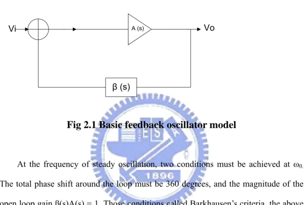
An oscillator circuit can be viewed as feedback circuits as shown in Fig 2.1. Consider the simple linear feedback system with the transfer function.
) ( ) ( 1 ) ( s A s s A Vi Vo β − =
β (s) A (s) Vo Vi
Fig 2.1 Basic feedback oscillator model
At the frequency of steady oscillation, two conditions must be achieved at ω0.
The total phase shift around the loop must be 360 degrees, and the magnitude of the open loop gain β(s)A(s) = 1. Those conditions called Barkhausen’s criteria, the above conditions imply that any feedback system can oscillate if its loop gain and phase shift are chosen properly. After shifting around 360 degrees, the signal adds to the previous signal and enhanced it so that the circuit appears oscillation.
In most RF oscillators, however, a frequency selective network called a
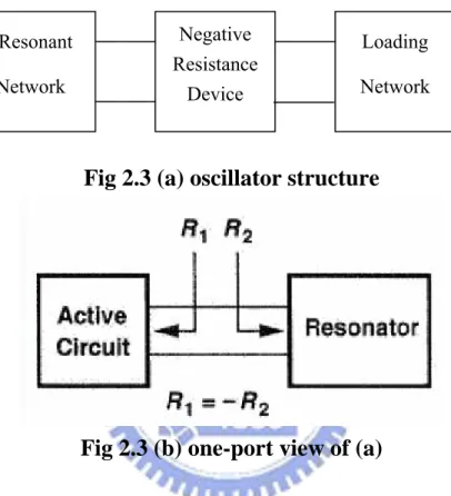
“resonator”, a tunable LC tank is included in the loop so as to stabilize the selected frequency as shown in Fig 2.2.
Fig 2.3 (a) oscillator structure
Fig 2.3 (b) one-port view of (a)
The above view of oscillators is called two-port model in microwave theory because the feedback loop is closed around a two-port network. By contrast the one-port model treats the oscillator as two one-port networks connected to each other as shown in Figure 2.3(b) The tank by itself does not oscillate indefinitely because some of the stored energy is dissipated in R1 in every cycle. The idea in the one-port model is that
an active network generates impedance equal to −R1 so that the equivalent parallel
resistance seen by the intrinsic, lossless resonator is infinite. In essence, the energy lost in R2 is replenished by the active circuit in every cycle, allowing steady
oscillation [1]. Resonant Network Negative Resistance Device Loading Network
2.2 Parameters Issue
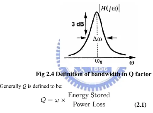
2.2.1 Quality Factor
Traditionally, phase noise of LC oscillators usually depends on their Q. Intuitively; higher Q of the LC tank is better, the sharper the resonance and the lower the phase noise skirts. Resonant circuit usually exhibit a bandpass transfer function. The Q can also be defined as the “sharpness” of the magnitude of the frequency response. In Fig 2.12, Q is defined as the resonance frequency divided by the two side -3 dB bandwidth.
Fig 2.4 Definition of bandwidth in Q factor
Generally Q is defined to be:
(2.1)
For an electrically resonant system, the Q factor represents the effect of electrical resistance. In a series RLC circuit,
C L R
Q= 1
(2.2)
The higher Q indicates a lower rate of energy dissipation relative to the oscillation frequency. We always have to design the better QTank when we do the optimization
2.2.2
Tuning range and K
VCOof Oscillators
In recently years, cellular phone systems such as W-CDMA must support multi-band or multi-mode operation. For a cost-effective W-CDMA RFIC that supports multi-band UMTS, a single VCO generating LO signals, which has a wide frequency range and attains low phase noise at low power.
A wide tuning range LC-tuned voltage controlled oscillator featuring small VCO-gain (KVCO) fluctuation was developed. For small KVCO fluctuation, a serial LC-resonator that consists of an inductor, a fine-tuning varactor, and a capacitor array was added to a conventional parallel LC-resonator that uses a capacitor array scheme. A general approach to achieving both wide frequency tuning range (Δf) and low
KVCO in a VCO is to use a array of switching capacitors. However, KVCO fluctuates
widely in the oscillation frequency range of the VCO, thereby degrading the performance of the PLL. The KVCO fluctuation increases with Δf of the VCO, so it must be suppressed when wide Δf is necessary. There are several tuning methods talked about in [5]. The principle of switched tuning element to cover a wide frequency range is shown in Fig 2.5.
2.3 Varactor
2.3.1 Diode Varactor
Fig 2.6 Reversed-Biased PN Junction
m B R V C C ⎟⎟ ⎠ ⎞ ⎜⎜ ⎝ ⎛ + = φ 1 0 var
(2.3)
When a reverse voltage is applied to a PN junction, the holes in the p-region are attracted to the anode terminal and electrons in the n-region are attracted to the cathode terminal creating a region where there is a little current. This region, the depletion region, is essentially devoid of carriers and behaves as the dielectric of a capacitor. The depletion region increases as reverse voltage across it increases; and since capacitance varies inversely as dielectric thickness, the junction capacitance will decrease as the voltage across the PN junction increases.
PN junctions suffer from a limited tuning range that trades nonlinearity in the
C-V characteristic. The capacitance varies under reverse bias and sharply under forward bias.
2.3.2 MOSFET Varactor
Fig 2.7 Nonlinear C-V characteristic
The varactor can be operated in either accumulation mode or strong inversion mode. The device suffers from a large source-drain resistance in the vicinity of minimum capacitance due to the low carrier concentration in the channel.
Fig 2.8 Accumulation mode MOS varactor
A MOS transistor with drain, source, and bulk (D, S, B) connected together realizes a MOS capacitor with capacitance value dependent on the voltage Vgs between S and gate (G). Since the material under the gate oxide is n-type, the concept of strong inversion does not apply here.
A three-terminal varactor such as a MOSFET can decouple the signal and the control, in that the control voltage might be the bias across the substrate and shorted
source-drain, while the oscillation appears across the gate and source-drain [Fig 2.9]. The standalone varactor is specified by its small-signal, or incremental capacitance CSS versus VC. This is defined in terms of the instantaneous charge Q and voltage V
across the varactor as follows:
dV dQ
CSS = When V=VC
(2.4)
Fig 2.9 Typical oscillation waveform of MOS varactor , ref [6]
We know the effective capacitance is composed by time-average capacitance and nonlinear varactor driven by oscillation. This leads to the frequency-tuning characteristic of the oscillator. It’s depends on the amplitude of oscillation.
2.3.3 AM-FM Conversion
An undesirable side effect associated with a varactor is that its
effective capacitance depends not only on control voltage, but also on the
amplitude of oscillation. Usually, AM noise can later be stripped off in a
limiter to restore the close-in spectral purity of the oscillation. However,
these amplitude fluctuations also modulate the effective capacitance of a
varactor, which then converts AM noise into FM noise [6].
In physical view, fluctuations in oscillation amplitude due to noise
can cause fluctuations in effective capacitance and thus in frequency, a
process called AM-to-FM conversion. The wider frequency tuning range,
the stronger the varactor’s proclivity to convert AM into FM.
Thus, we have to retard the slope of C-V curve and make it more
linear if we want to have good performance on phase noise of VCO.
2.4 Inductor
2.4.1 Inductor
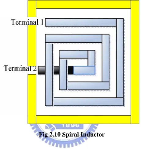
Fig 2.10 Spiral Inductor
In integrated RF works in silicon, inductors are normally implemented as a planar spiral-shaped metal. Figure 2.10 shows the top view of an example spiral inductor in silicon, realized using the top metal layer while the metal layer below the top metal layer is used for an interconnection for terminal 2. The loss of inductor comes from low-frequency resistivity, skin effect, and substrate loss. Substrate loss due to both magnetic coupling and capacitive coupling are eddy current and displacement current flows in the substrate. In order to reduce the loss, a conductive shield can be placed under the inductor. We often consider the n-well, silicided polysilicon, and metal layers for pattern ground shield.
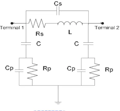
Fig 2.11 Simple equivalent model of Spiral Inductor
Fig 2.11 includes parasitic capacitance resulting from the underpass wire connecting the inner end of the inductor and the fringing capacitance. The line must be sufficiently so that Rdc does not significantly limit the Q.
2.4.2 Transformer
Transformer has been used in radio frequency (RF) circuits since the early days of telegraphy. Recent work has shown that it is possible to integrate passive transformers in silicon IC technologies that have useful performance characteristics in the radio-frequency range, opening up the possibility for IC implementations of narrowband radio circuits [7].
Fig 2.12 (a) Transformer layout (b) Schematic symbol ref. [8]
The operation of a passive transformer is based upon the mutual inductance between two or more conductors, or windings. The transformer is designed to couple alternating current from one winding to the other without a significant loss of power.
It’s hard to achieve a higher quality factor inductor in the on-chip fully integrated IC. The Q factor is constrained by conductor losses arising from metallization resistance, the conductive silicon substrate, and substrate parasitic capacitances (which lower the inductor self-resonant frequency). Several approaches have been used to improve the Q factor of monolithic inductors in silicon.
Fig 2.13 (a) Low frequency model (b) High frequency model ref. [8]
By using transformer, we always can improve the quality factor of inductor to make the performance better. There are many variable topologies of transformer; it makes circuit design more creative by using monolithic transformer. There are also some special transformer feedback techniques applying in novelty circuit.
P S S P P S
L
L
i
i
v
v
n
=
=
=
(2.5)
S P mL
L
M
k
=
(2.6)
We can calculate the coarse parameter about transformer designation easily by using the model as shown in Fig 2.12. The turn ratio is an important issue when we have to do matching network or coupling considerations. Transformer also can be a balun to transfer signal, either be a combiner to combine the energy.
(a)
(b)
Fig 2.14 (a) Two asymmetrical inductor (b) a symmetrical inductor
ref. [9]
The monolithic inductor is a microstrip transmission line with an ratio L/C that favors inductance over capacitance. For differential excitation, these parasitic have higher impedance at a given frequency than in the single-ended connection. This reduces the real part and increases the reactive component of the input impedance. Therefore, the inductor is improved when driven differentially, and the self-resonant
frequency (or usable bandwidth of the inductor) increases due to the reduction in the effective parasitic capacitance in the effective parasitic capacitance from Cp+Coto
Co
Cp/2+ in the Fig. 2.13 [9]. By using the structure, it reduces the half area and
improves the Q about two times (ideally). It’s a popular structure when designing the differential circuit.
(a)
(b)
(c)
Fig 2.15 (a) Lump-circuit model (b) single-ended (c) differential
excitation ref. [9]
2.5 Phase Noise
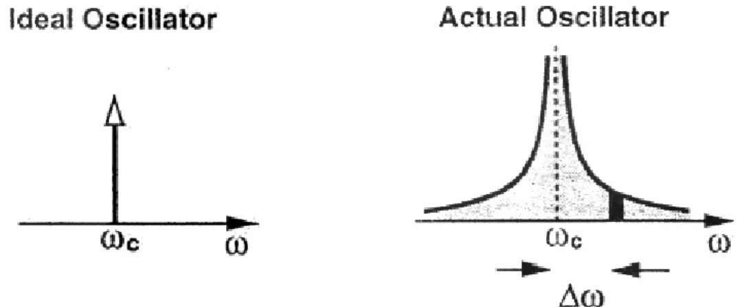
Fig 2.16 (a) Spectrum of ideal Oscillator (b) Spectrum of actual
Oscillator
In RF applications, phase noise is usually characterized in the frequency
domain. For an ideal sinusoidal oscillator operating atωC, the spectrum assumes the shape of an impulse which contains only a single spectral line at the nominal frequency. In reality, the spectrum of actual oscillator exhibits skirts around the carrier frequency (Fig 2.14). To quantify phase noise, we consider a unit bandwidth at an offset Δw with respect toωC , calculate the noise power in this bandwidth, and divide the result by the carrier (average) power:
2.5.1 Noise Source
Because of the large signal operation in oscillator, the low frequency noise would have been upconverted to the carrier frequency sideband from the nonlinear characteristic.
For realizing the phase noise further, we talk about the noise source of MOSFET. There are three major noise known as thermal noise, shot noise, flicker noise. Thermal noise is produced by conductivity; it’s proportional to temperature with a flat power density spectral. Shot noise is produced by the PN junction with current flow; it’s proportional to average current with flat power density spectral too. The third, flicker noise is produced by the process of trapping and releasing of carrier. It has f −α spectral, α ≅1, PMOS has a lower flicker noise than NMOS because of
the electrical hole is harder to catching than electronics. The effective mean-square in
) noise power spectral of MOS channel thermal noise is: n m g kT f i γ 4 = Δ
(2.8)
γ is relative to the MOS channel length, γ ≅2/3~3,γ =2/3 when long channel operation, the shorter channel, the largerγ . The flicker noise power density spectral at drain output can be presented [2]:
OX m n WLC g f K i 2 2 = ⋅
(2.9)
From (2.8) and (2.9), we can find the corner frequency: γ α KT WL C g K f OX m C 4 ⋅ ⋅ =
(2.10)
Larger MOSFETs exhibit less 1/f noise because their large gate capacitance smoothes the fluctuations in channel charge. Hence, if good 1/f noise performance is
to be obtained from MOSFETs, the largest practical device sizes must be used (for a given gm). In an ideal oscillator, the only noise source is the noise of the parallel resonator conductance, thus it is the white thermal noise. The single sideband noise spectral density is:
{ }
⎥
⎥
⎦
⎤
⎢
⎢
⎣
⎡
⎪⎭
⎪
⎬
⎫
⎪⎩
⎪
⎨
⎧
⎟⎟
⎠
⎞
⎜⎜
⎝
⎛
Δ
+
=
Δ
2 02
1
2
log
10
f
Q
f
P
FkT
f
L
sig(2.11)
2.5.2 Lesson’s Model
Phase and frequency fluctuations have therefore been the subject of numerous studies. Although many models have been developed for different types of oscillators, we always depict the phase noise of oscillator with Lesson’s theory at early stage [10]. Lesson’s theory predicts the double-sideband noise spectral density as:
{ }
⎥
⎥
⎦
⎤
⎢
⎢
⎣
⎡
⎟
⎟
⎠
⎞
⎜
⎜
⎝
⎛
Δ
Δ
+
⎪⎭
⎪
⎬
⎫
⎪⎩
⎪
⎨
⎧
⎟⎟
⎠
⎞
⎜⎜
⎝
⎛
Δ
+
=
Δ
f
f
f
Q
f
P
FkT
f
L
f sig 3 / 1 2 01
2
1
2
log
10
(2.12)
Where:K is the Boltamann’s constant, T0 is the standard noise temperature, F is the excess noise factor,
f0 is the oscillator frequency,
QL is the loaded Q
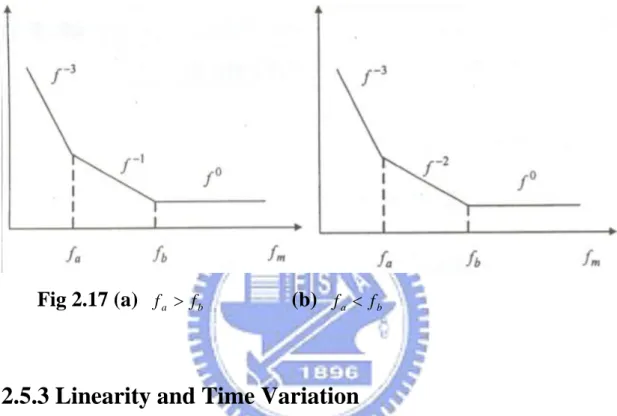
a f f
f1/ 3 = is the corner frequency, where the slope of the phase noise spectral
density changes from -30dB/dec. to -20dB/dec.
The bandwidth of resonator isBW = f0 /QL, the half BW is f . Ifb fa > fb, the
resonator has higher QL, the behaviors of phase noise curve as shown in 2.15(a).
2.15(b). There exists the curve proportional to −3
f slope at the low offset frequencies
from the carrier f . In this region, the phase noise is caused by the active device 0
flicker noise which denoted by 1/f noise. The F factor is a empirical parameter here. Thus we can only observe the trend of phase noise, but not calculate it accurately.
Fig 2.17 (a)
fa > fb(b)
fa < fb2.5.3 Linearity and Time Variation
Lesson’s model describes the curve of phase noise, but there still exists questions such as the unknown F factor, fa ≠ f1/f. Most of these models are based
on a linear time invariant (LTI) system assumption and suffer from not considering the complete mechanism by which electrical noise sources, such as device noise, become phase noise. Since any oscillator is a periodically time-varying system, its time-varying nature must be taken into account to permit accurate modeling of phase noise.
Fig 2.18 (a) maximum voltage response (b) zero crossing response
The ideal lossless oscillator is injected by an impulse as shown in Fig 2.18. We observe the different point of time. Injecting into the point of maximum voltage, it’s make only the amplitude changes in Fig 2.18(a). When the zero crossing is affected, the injection changes only the output phase. Both the amplitude and phase changes would be observed. An Impulse Sensitivity Function (ISF) describes the phase sensitivity of this phenomenon. Due to the stability oscillation limitation make the constant oscillation without affecting by impulse, but the changes of phase will continue. Its ISF is also periodic and thus it can be spread out to the Fourier series with coefficients characterizing individual harmonic components. All harmonics affects the phase modulation with the carrier frequency. Low frequency noise is up-converted to the nominal frequency and is weighted by the coefficient c0. The
noise near carrier frequency is weighted by c1. Others harmonics undergoes
down-conversion, turning into noise in the 1 f region, are weighted by their / 2
Fig 2.19 Conversion of noise to phase fluctuations and phase
noise sidebands, ref [11]
Consider the random noise current in(t) whose power spectral density has both a flat region and a 1/f region, as shown in Fig 2.19. The noise component located near integer multiples of the oscillation frequency is transformed to low 0the spectrumSV(ω). ISF has to be minimized due to the phase noise minimizing. The
2
/
1 f region arises from white thermal noise may be expressed as [10]:
⎥ ⎥ ⎥ ⎥ ⎥ ⎦ ⎤ ⎢ ⎢ ⎢ ⎢ ⎢ ⎣ ⎡ Δ Γ Δ ⋅ = Δ 2 2 max 2 2 log 10 ) ( ω ω q f i L rms n
(2.13)
Where Γ is the root mean square value of the ISF. The area rms
3
/
1 f that originates from the flicker noise up-conversion may be expressed as [10]:
⎥ ⎥ ⎥ ⎥ ⎥ ⎦ ⎤ ⎢ ⎢ ⎢ ⎢ ⎢ ⎣ ⎡ Δ Δ ⋅ Δ ⋅ ⋅ = Δ 2 2 max / 1 2 2 0 8 log 10 ) ( ω ω ω ω q f i c L f n
(2.14)
The phase noise 1 f corner is the frequency where the sideband power due to the / 3
corner in the phase noise spectrum: 2 1 2 0 / 1 / 1
2
1
3c
c
f f=
ω
⋅
ω
(2.15)
Obviously,
ω
1/f3 ≠ω
1/f , even though smaller than 1/f corner very much. It’s differentwith Lesson’s theory. If we want to get lower phase noise, we should make c 0
smaller, that’s mean the Γ function waveform should be more symmetrical [11]. There are several noise sources in the voltage controlled oscillator such as flicker noise of active device, resonator loss, bias source, AM-FM from varactor, substrate coupling noise. The designers always have to do some trade-off between power, frequency, tuning range, and phase noise. The more we know about the rules and trend of phase noise, the more optimization conditions we can control.
CHAPTER 3 CMOS LC TANK OSCILLATOR
This chapter talks about the theory of LC tank oscillator. It also introduces several kinds of LC oscillators fabricated by CMOS. Analyze the advantage and drawback of its structure. We discuss their novel designs about the improvement of VCO characteristics. Basically, the design considerations of a VCO design always takes care of phase noise, Quality value, power consumption and tuning range.
3.1 Negative-R
Oscillators
Fig 3.1 Equivalent Model
If a one port circuit exhibiting a negative resistance is placed in parallel with a tank, the combination may oscillate. Because of the effective power will be replenished and consumed at the same time when negative resistance exists in the circuit.
1 1
V
gm
2 2V
gm
Ix
+
−
+
−
2 V1
V
2 1 2 1 gm Ix gm Ix V V Vx= − =− − gm gm gm Ix Vx 1 1 2 2 1 − = ⎟⎟ ⎠ ⎞ ⎜⎜ ⎝ ⎛ + − = (If gm1 = gm2 = gm) (3.1)
Voltage Controlled Oscillator
0 V1 V2 f0 f1 f2 fout Vcont B
Fig 3.3 (a) voltage control frequency (b) f-V relationship
LpCp
f0 = 1 (3.2)
KvcoVcont f
fout = 0 +
(3.3)
Kvco
:
Gain or Sensitivity of VCOAn ideal voltage-controlled oscillator is a circuit whose output frequency has a linear variation related to its control voltage. For a given noise amplitude, the noise in the output frequency is proportional toKvco
.
Thus the VCO sensitivity must beminimized to minimize the noise effect of noise on Vcont. This is a trade-off among tuning range and phase noise.
VCO
3.2 Differential LC-Tank Voltage Controlled
Oscillators
Fig 3.4 (a) differential VCO (b) differential VCO with tail current
0 2 2 − ≥ gm Rp gm Rp ≥ − 1 (3.4)
If the small-signal resistance presented by cross-coupled pair NMOS to the tank is less negative than –Rp, then the circuit experiences large swings such that each transistor is nearly off for part of the period. Thus the oscillation process would be a dynamic balance without producing infinite amplitude, thereby yielding an average resistance of –Rp. There is some analysis about oscillation condition:
Fig 3.5 Nonideal LC tank model
From the derivation process, we know that gm must be large than
Rp
1
so that the oscillator work. Thus we have to enhance device scaling to increase gm, or reduce Rs from inductor and capacitor to increase Rp. But the parasitic effect also becomes large when device scaling increase and the loss from metal increase in high frequency. We also can raise the supply voltage to increase gm. But it makes more power consumptions. That’s why high frequency circuit is more difficult to design than low
0 1 tan ≤ + − − = Rp gm gm Rp R k 1
Rp
gm
≤
−
1
(From inductor)
(3.5)(From capacitor)
(3.6)frequency circuit. We always have to do some trade-off, find the optimization of the circuit.
There are two conventional differential cross-coupled pair VCOs shown in Fig 3.4. This is the most popular structure for high frequency VCO design because of its smaller negative
gm
1
− makes the oscillation condition become easier to achieve. In order to alleviate noise coupling, it is preferable to employ differential paths for both the oscillation signal and the control line. With the differential signal, output amplitude can be combined to achieve large output oscillation amplitude, thus making the waveform less sensitive to noise.
Each structure of Fig 3.4 has its advantage and drawback. The structure in Fig 3.4(a) is more sensitive to Vdd so that power consumption is hard to limit. Thus we have to reduce the device size to suppress the power consumption, but flicker noise increases at the same time. The structure in Fig 3.4(b) can limit the power consumption with a bias current, but the tail current has its flicker noise, it’s also a effective noise source to VCO too. We will mention these two structure later.
3.3 Phase Noise Operation in Differential LC-Tank Voltage
Controlled
Oscillators
In a current-biased differential LC oscillator, the nonlinearity stems from bias current exhaustion when the differential pair is biased at low currents. The differential pair sustains the oscillation by injecting an energy-replenishing square-wave current into the LC tank. As the tail current raised, the oscillation also raises, approaching single-ended amplitude ofVDD, negative peaks momentarily force the current-source
transistor into triode region. This is a self-limiting process.
From [15], we know the physical mechanisms of phase noise at work in the differential LC oscillator. The noise factor F is:
g R V IR F mbias 9 4 4 1 0 γ π γ + + = (3.7)
The expression in (3.7) describes three noise contributions, respectively, from the tank resistance, the differential-pair MOSFETs, and from the current source. The thermal noise in the differential MOSFETs produce oscillator phase noise that is independent of the device size. In typical oscillators, the current-source contribution dominates other sources of phase noise. If the differential pair is switched to one side or the other, there is no differential output noise. Therefore, the oscillation samples the FET noise at every differential zero crossing.
Table 3.1 Comparisons of VCO structure in Fig 3.4
No Current Source Current Source
First MOSFET Triode Triode
As shown in Fig 3.4(a), we note VGD the oscillation of the two FETs to be equal
in magnitude but with opposite signs to the differential voltage across the resonator. At zero differential voltage, both switching FETs are in saturation, and the cross-coupled transconductance offers a small-signal negative differential conductance that induces startup of the oscillation.
As the rising differential oscillation voltage crossesV , the t VGD of one FET
exceeds+ , forcing it into the triode region, and Vt VGD of the other FET falls
below− , driving it deeper into saturation. TheVt gDSof the FET in triode grows with
the differential voltage, and adds greater loss to the resonator because the current flowing through it is in-phase with the differential voltage. In the next half cycle,
DS
g of the other FET adds to resonator loss. The two FETs lower the average
resonator quality factor over a full oscillation cycle.
As shown in Fig 3.4(b), when the differential voltage drives one FET into triode, it turns off the other FET. As no signal current can flow through thegDSof the triode
FET, this FET does not load the resonator [16]. The phenomenon of operation is shown in Fig 3.6; the load impedance will affect the effective quality factor of the resonator.
We can see the comparisons in Table 3.1. It is evidently the structure with current source is better choice for good phase noise performance. But there is still a problem shown in the third term of (3.7). The external phase noise comes from thermal noise in the current-source transistor around the second harmonic of the oscillation causes phase noise. We can use the noise filtering technique to remove the noise source as shown in Fig 3.7 [16]. Thus, the structure is popular for the designers using to make the performance better and limit the power consumption. But it costs more area in the chip. This is the worst drawback of this structure.
3.4 Transformer Feedback Voltage Controlled Oscillator
The complementary cross-coupled topology with transformer structure shown in Fig 3.7 achieves a lower phase noise than an NMOS topology for the same power. The resonator tank is formed with an integrated transformer with two sets of varactors, it’s a combination of traditional structure and transformer. The transformer-based design results in a much sharper impedance and phase response around the resonant frequency [17]. It’s a quality factor enhancement technique. When designing low frequency circuit, the effective inductance of the resonator can be enhanced with using the smaller area transformer. But in higher frequency, it’s a limitation for designation.
3.4.1 Drain-Source Transformer Feedback VCO
Fig 3.9 (a) Drain-Source Feedback VCO (b) Voltage Waveform
To improve the VCO performance in terms of low supply voltage, low power with the differential transformer structure, and low phase noise, a TF-VCO is proposed to provide extra voltage swings, improved loaded quality factor, and minimum noise-to-phase-noise transfer. With the transformer feedback, the drain voltage could swing above the supply voltage and the source voltage could swing below the ground potential, and most importantly, the drain and source signal oscillate in phase. It makes the oscillation amplitude is enhanced, and consequently, the supply voltage can be reduced for the same phase noise with lower power consumption or for better phase noise with the same power consumption [18]. Thus, this is a novelty design for voltage-controlled-oscillator, but there is also some limitation in operating frequency because of the parasitic capacitor and the effective inductance.
3.4.2 Drain-Gate Transformer Feedback VCO
Fig 3.10 (a) Drain-Gate TF-VCO (b) Complementary VCO with
Drain-Gate Transformer Feedback
The drain-gate transformer feedback configuration proposed in Fig 3.9(a) [19]. This makes use of the quality factor enhancement in the resonator using a transformer and the deep switching-off technique by controlling gate bias. In order to design VCO with low phase noise performance, there are three considerations depicted in [19]. The most useful improvement is the reduction of the noise of active device. The deep-turn-off of switching pair is important when they are at off state. Drain and gate dc-biases are separately controlled to have feedback signals bias-level shifted. It has been known that 1/f noise can be reduced by lowering gate to source voltage v of gs
switching pair at off state [20].
In the topology shown in Fig 3.9(b) [21], the gate bias can be used to limit the output dc level to half ofVDD, which results in the highest output signal power for a
give bias. The current source can be removed, and thus both phase noise and power consumption can be improved. These two structures are useful for reducing phase
noise, but there isn’t lower power consumption at the same time.
3.4.3 Back-Gate Transformer Feedback VCO
Fig 3.11 Back-Gate Transformer Feedback VCO
This topology can oscillate at higher frequency while keeping comparable performances compared to those of the other topologies discussed before because of the considerations of transformer turns ratio [22].
topologies.
This simulation based on the same level of output swing and almost the same oscillation frequency compared to the VCO with source feedback. The VCO with front-gate transformer feedback has an oscillation frequency that is 3 GHz lower compared to whose of the other topologies. It seems have a better performance compared with other structures. But there are some issues which aren’t mentioned in the simulation, such as power consumption, the turn’s ratio. The comparison may be not a convincible result.
We want to figure out a suitable design of those architectures. From the discussion we talked about before. We know that the transformer-feedback VCO can achieve the same effect to turn off switching pair MOSFET without using bias current source. Thus, we can remove a noise source without using filtering technique; it does can reduce the area of chip size. The lowest power consumption one of these structures is drain-source coupling of transformer feedback, and its have higher output swing to increase signal-to-noise-ratio to reduce phase noise. The most potentially circuit can be improving to be a better design.
Chapter 4 SIMLATION AND MEASUREMENT
The 10 GHz Ultra-Low-Power differential VCO with
Transformer Feedback
4.1 Proposed Design
Low voltage operation of analog circuits is a important factor for low-power system-on-chip designation. Low voltage, however, limits the signal amplitude, which in turn limits the signal-to-noise ratio and degrades system performance. It’s also could be achieved by using silicon-on-insulator (SOI) [23], external inductor with high quality factor [24] etc, however, are not fully compatible to standard CMOS process.
There are many structures to improve VCO as shown before in Chapter3. Considering low-power methods, we try to improve the structure in section 3.41. Based on transformer-feedback VCO, we can easily design the low supply voltage circuit. But in higher frequency circuit, it’s still not enough to achieve low power and high performance at the same time. Thus, we figure out other way to increase the gm to improve signal-noise-ratio. We have done it without adding additional supply voltage by using body bias to reduce the MOS threshold-voltage (Vth).
(4-1)
We have done an easy comparison of combination in these two structures as shown in Fig 4.1. As a result of Fig 4.2, we know that these two structures are useful.
Fig 4.1 (a) Add body bias on NMOS (b) Add body bias on NMOS
with transformer feedback
Table 4.1
transconductance comparison
VB 0 0.1 0.2 0.3 0.4 0.5
Gm1(mA/V) 3.1 4.2 5.5 6.6 7.6 8.3
Gm2(mA/V) 3.8 5.2 6.8 8.8 9.5 10.4
Fig 4.3 Proposed Circuits
Forward body bias VB,Vdd =0.5V , gm is very small when VB= 0
Gm1: gm of Fig 4.1(a)
The design takes advantage of higher quality factor of differential transformers over simple single-ended inductors for differential circuit. For differential transformers in Fig 4.4, the quality factor is improved by magnetic coupling of two coils ideally increase the inductance value while series loss is unchanged. And this four port transformer with M5 and M6 broadside couple effect can reduce the series loss of the structure at the same time.
Fig 4.4 Four port broadside couple transformer
Table 4.2 Q comparison of transformer
L
Q
(single)
Q
(differential)
Primary 0.39nH 8.7
15.5
Second 0.21nH 6.6
12.7
4.2 Simulation
Fig 4.5 Waveform
4.3 Measurement
Using Agilent E4440A Spectrum Analyzer & Agilent
E5052A Signal Source Analyzer (SSA)
Fig 4.8 Spectrum
-0.5 -0.4 -0.3 -0.2 -0.1 0 0.1 0.2 0.3 0.4 0.5 9.4 9.6 9.8 10.0 10.2 10.4 Y Axi s T itl e X Axis Title BFig 4.9 Tuning Range
Fig 4.10 Phase noise
Table 4.3 Specification
規格 CMOS 0.18 m 結果比較 量測 模擬 Frequency (GHz)@(Vc=0~0.5) 9.46~10.21 9.57~10.35 Frequency (GHz)@(Vc=-0.5~0.5) 9.46~10.41 NA Phase noise (1MHz) @(Vc=0~0.5) -112.49 -113 Tuning range(GHz) 9.6% 7.8% Pdiss (total) (mW) 1.3~1.5 0.7~1 Die size (mm2) 0.61x0.85=0.5185Fig 4.11 Layout
CHAPTER 5 Design Flow
5.1 Design Flow
The simulation software ADS designer is used to design the circuit. ADS momentum is used to do EM simulation. After the layout of circuit is finished, DRC & LVS & LPE is done to check the correction for the design.
Specification
Literature survey
Circuit design
Simulation & Optimization
Layout and Check (DRC, LVS)
Post-Simulation
Finish
Fit Spec NO YES Fit Spec YES NOCHAPTER 6 Conclusions & Improvement
6.1 Conclusion
As a consideration of high frequency, small area, low-phase noise and low-power, there aren’t many architectures could satisfy the conditions. A transformer-feedback voltage-controlled oscillator is proposed as the structure choice for low-voltage, low-power, and low-phase-noise application. Transformer feedback enables to increase output swing by the dual signal swings across the supply voltage and the ground potential. The design also provides higher quality factor to improve phase noise and the power consumption.
The measurement results show that the oscillation frequency is 10 GHz with 9.6% tuning range. The core dc power consumption is only 1.3mW. The phase noise at 1-MHz offset is -112.49 dBc/Hz. The chip size is 0.51 2
mm , core size is only
0.063 2
mm .
To realize the integrated RF circuits with the good performances, the monolithic inductor with good quality factor is an essential requirement, especially for phase noise of VCO. In the passive components, the differential type inductor and deep-trench inductor are the better choice in Q-enhancement. Symmetrical differential inductor is the best choice since it has higher quality factor, resonant frequency and small die area [9]. Every circuit combined with passive and active device. The improvements in both of them are important for our design. The physics is limited, but the idea is infinite. We always try to combine some useful improvement and concepts, no matter how strange the idea is.
(6.1)
(6.2)
Table 6.1 the comparisons with others literatures
Ref Process Freq (GH z) FTR(%) Phase Noise@1 MHz VDD P(mW) FOM1 FOM2 3 0.18um 15 1.6 -112 2 52 -177 161.1 4 0.18um 21.3 3(-1~1.5v) -105.9 2.4 9.6 -182.8 172.3 5 0.18um 17 16.5 -110 1 5 -187.6 -191.9 6 0.18um 10.3 11.1 -118.7 1.8 11.8 -188.2 -189.1 7 0.13um 28 6.7 -112.9 1.2 12 -190 -186.5 8 0.18um 11 2.6 -109.4 1.8 3.8 -181.8 -170.1 9 0.18um 10 12.5(-1~1.5v) -118.7 1.8 6.6 -187.9 -189.8 Post-sim. 0.18um 9.9 7.8@(0~0.5V) -113 0.5 0.7 -194 -192
This work 0.18um 9.9 9.56@(-0.5~0.5V) -112.49 0.5 1.3 -191 -190.6
{ }
⎟ ⎠ ⎞ ⎜ ⎝ ⎛ + ⎭ ⎬ ⎫ ⎩ ⎨ ⎧ Δ − Δ = mW P f f f PN FOM o dc 1 log 10 log 20 1 ⎟ ⎠ ⎞ ⎜ ⎝ ⎛ − = 10 log 20 1 2 FOM FTR FOM6.2 Improvement
There is an issue on Substrate noise coupling effect.With the metal interconnects linked to the transistors and varactors, the noise collected by the inductor can be an important contributor to the undesired spurs in addition to the direct coupling through the body of the nonlinear devices. A straightforward solution is to use a DNW layer to prevent the noise coming from the substrate. Both of two structures provide the isolation of noise. The DNW structure has been widely used to reduce undesired interference as shown in Fig 5.1(a). [25]
Fig 5.1 (a) DNW inductor (b)
Patterned Ground Shields inductor
Another structure, PGS, is also employed to reduce the substrate noise coupling. With the metal strips placed underneath the inductor, the PGS structure has been used to increase the inductor quality factor, owing to the reduced image current [26]. We can improvement our circuit with PGS under the inductor.
Reference
[1]B. Razavi, RF microelectronics, Prentice Hall PTR, 1998.
[2] Thomas H. Lee, “The Design of CMOS Radio-Frequency Integrated Circuit 2nd edition”.
[3]J.C. Guo, C. H. Huang, K. T. Chan, W. Y. Lien, C. M. Wu, and Y. C. Sun, “0.13μm low voltage logic base RF CMOS technology with 115GHz fT and 80GHz fMax,” 33rd European Microwave Conference, pp. 682-686, 2003.
[4]B. Razavi, Design of analog CMOS integrated circuits, McGraw-Hill, 2001.
[5]A. Kral, F. Behbahani, and A.A. Abidi, “RF-CMOS Oscillators with Switched Tuning,” IEEE Custom Integrated Circuits Conf., Santa Clara, CA, 1998, pp. 555-558
[6] E. Hegazi, A. A. Abidi, “Varactor Characteristics, Oscillator Tuning Curves, and AM-FM Conversion,” in Proc. IEEE J. Solid State Circuit, vol. 38, pp. 1033-1039, June 2003
[7]M. Hershenson, S. S. Mohan, S. P. Boyd, and T. H. Lee. “Optimization of inductor circuits via geometric programming,” in Proc. Design Automation Conf., 1999, pp. 994-998
[8]J. R. Long, “Monolithic transformers and their application in a differential CMOS RF low-noise amplifier,” IEEE J .Solid-State Circuits, vol. 35, pp.1368-1382, Sep. 2000
[9]M. Danesh, J. R. Long, “Differential Driven Symmetric Microstrip Inductors,”
IEEE Trans. Microwave Theory Tech., vol. 50, no. 1, pp.332-341, Jan. 2002
[10]D. B. Leeson, “A simple model of feedback oscillator noises spectrum,” Proc.
IEEE, vol. 54, pp. 329-330, Feb, 1966
[11]A. Hajimiri, T. H. Lee, “A general theory of phase noise in electrical oscillators,”
[12]O.Baran, M. Kasal, “Oscillator Phase Noise Models,” Radioelektronika pp. 1-4, April. 2008
[13]A, Jerng, C. G. Sodini, “The impact of device type and sizing on phase noise mechanisms,” IEEE J. Solid-State Circuits, vol. 40, p. 360-369, Feb. 2005
[14]D. Ham, A. Hajimiri, “Concepts and Methods in Optimization of Integrated LC VCOs,” IEEE J. Solid-State Circuits, vol. 36, pp. 896-909, June 2001
[15]J. J. Rael, A. A. Abidi, “Physical process of phase noise in differential LC oscillators,” in Proc. IEEE Custom Integrated Circuits Conf., Orlando, Fl, 2000, pp.569-572
[16]E. Hegazi, H. Sjoland, A. A. Abidi, “A filtering technique to lower LC oscillator phase noise,” in Proc. IEEE J. Solid-State Circuits, vol. 36, pp. 1921-1930, Dec. 2001 [17]M. Straayer, J. Cabanillas, and G. Rebeiz, “A low-noise transformer-based 1.7-GHz CMOS VCO,” in Proc. IEEE Int. Solid-State Circuits Conf. (ISSCC) Dig.
Tech. Papers, Feb. 2002. pp. 286-287
[18]K. Kwok, H. C. Luong, “Ultra-low-voltage high-performance CMOS VCOs using transformer feedback,” IEEE J. Solid-State Circuits, vol. 40, no. 3, pp. 652-660, March 2005
[19]D. Baek, T. Song, E. Yoon, and S. Hong, “8-GHz CMOS quadrature VCO using transformer-based LC tank,” IEEE Microw. Wireless Compon. Lett., vol. 13, no. 10, pp. 446-448, Oct. 2003.
[20]S. L. J. Gierkink, E. A. M. Klumperink, A. P. van der Wel, G. Hoogzaad, E. van Tuijl, and B. Nauta, “Intrinsic 1/f device noise reduction and its effect on phase noise in CMOS ring oscillators,” IEEE J. Solid-State Circuits, vol. 34, pp. 1022-1025, July 1999
[21]C.-C. Li, T.-P, Wang, C.-C. Kuo, M.-C. Chuang, and H. Wang, “A 21GHz Complementary Transformer Coupled CMOS VCO,” IEEE Microw. Wireless
Compon. Lett., vol.18, no. 4, April 2008
[22]N.-J. Oh and S.-G. Lee, “11-GHz CMOS differential VCO with back-gate transformer feedback,” IEEE Microw. Wireless Compon. Lett., vol. 15, no. 11, pp. 733-735, Nov. 2005
[23] M. Harada, T. Tsukahara, J. Kodate, A. Yamagishi, and J. Yamada, “2-GHz RF front-end circuits in CMOS/SIMOX operating at an extremely low voltage of 0.5 V,”
IEEE J. Solid-State Circuits, vol. 35, no. 12, pp. 2000–2004, Dec. 2000.
[24] A. Porret, T. Melly, D. Python, C. Enz, and E. Vittoz, “An ultralowpower UHF transceiver integrated in a standard digital CMOS process: architecture and receiver,”
IEEE J. Solid-State Circuits, vol. 36, no. 3, pp. 452–466, Mar. 2001.
[25]Y.-C. Wu, S. S. H. Hsu, K. K. W. Tan, and Y.-S. Su “Substrate noise coupling reduction in LC voltage-controlled oscillators,” IEEE ELECTRON DEVICE
LETTERS, VOL. 30, NO. 4, APRIL 2009
[26] C. Yue and S. Wong, “On-chip spiral inductor with patterned ground shields for Si-based RF IC’s,” IEEE J. Solid-State Circuits, vol. 33, no. 5, pp. 743–752, May 1998.
![Fig 2.9 Typical oscillation waveform of MOS varactor , ref [6]](https://thumb-ap.123doks.com/thumbv2/9libinfo/8151620.167115/21.892.151.605.271.827/fig-typical-oscillation-waveform-mos-varactor-ref.webp)
![Fig 2.19 Conversion of noise to phase fluctuations and phase noise sidebands, ref [11]](https://thumb-ap.123doks.com/thumbv2/9libinfo/8151620.167115/34.892.198.592.136.416/fig-conversion-noise-phase-fluctuations-phase-noise-sidebands.webp)
