國
立
交
通
大
學
電機學院微電子奈米科技產業研發碩士班
碩
士
論
文
不同表面處理對二氧化鉿與二氧化鋯推疊式高介電常
數材料薄膜之效果
The Effect of Various Surface Treatment to ZrO
2/HfO
2Stack Dielectric
Thin Films
研 究 生:李政勳
指導教授:張國明 教授
不同表面處理對二氧化鉿與二氧化鋯推疊式高介電常
數材料薄膜之效果
The Effect of Various Surface Treatment to ZrO
2/HfO
2Stack Dielectric
Thin Films
研 究 生: 李政勳 Student: Cheng-Hsun Lee
指導教授: 張國明 Advisor: Dr. Kow-Ming Chang
國 立 交 通 大 學
電機學院微電子奈米科技產業研發碩士班
碩 士 論 文
A Thesis
Submitted to College of Electrical and Computer Engineering National Chiao Tung University
in partial Fulfillment of the Requirements for the Degree of
Master In
Industrial Technology R&D Master Program on Microelectronics and Nano Sciences
January 2011
Hsinchu, Taiwan, Republic of China
中華民國一百年一月
I
不同表面處理對二氧化鉿與二氧化鋯推疊式高介電常
數材料薄膜之效果
學生: 李政勳 指導教授: 張國明 博士
國立交通大學電機學院產業研發碩士班
摘 要
隨著金氧半場效電晶體的微縮,傳統使用二氧化矽當作閘極介電
層將面臨到物理和電性的限制。當電晶體的閘極通道長度微縮到 100
奈米以下時,閘極介電層厚度將縮小至 1.2 奈米以下,以二氧化矽當
作氧化層將會面臨到很多的挑戰,影響最嚴重的就是太薄的二氧化矽
絕緣層會使大量載子直接穿隧造成大量的漏電流,為了有效抑制此漏
電流,需要使用高介電係數材料來取代二氧化矽作為閘極氧化層,高
介電係數氧化層可以在維持相同的等效氧化層厚度(維持相同的電容
值)的情況下,增加實際介電層厚度來抑制穿遂電流的形成。其中二氧
化鉿與二氧化鋯為主的材料被認為是目前最有可能來取代二氧化矽。
本研究製造了鈦-二氧化鉿-二氧化鋯-矽金屬絕緣層矽(MIS)結
構之電容,作為分析的樣品。首先,我們探討二氧化鋯介面層有無做沉
積後退火處理和矽表面上有無氟化處理的電性比較。接下來,在二氧
化鉿薄膜上,使用不同氣體(氮氣、氧化氮與氨氣)做不同時間下的電
漿處理,並且從這些不同條件中挑選最佳的電漿處理條件。最後,我
們比較了沒做任何處理、沉積後退火處理、氟化處理與氮化處理等不
同表面處理方法,探討對特性的影響。在論文中,由結果可以發現經
過退火與電漿處理後的介電質薄膜,可以得到較高的電容密度、較低
的漏電流以及較小的磁滯現象。這是因為退火處理可以有效改善薄膜
品質、電漿源中的氟原子可以抑制介電層和矽之間的氧化層成長並且
修復介電質中的缺陷,而氮原子可以修補介電層的缺陷。
III
The Effect of Various Surface Treatment to ZrO
2/HfO
2Stack Dielectric Thin Films
Student: Cheng-Hsun Lee Advisor: Dr. Kow-Ming Chang
Industrial Technology R & D Master Program of
Electrical and Computer Engineering College
National Chiao Tung University
Abstract
The aggressive scaling of MOS devices is quickly reaching the
fundamental and electric limits of convention SiO
2as the gate insulator.
When the gate length scales down below 100nm, the gate thickness will
scale down below 1.2 nm, the SiO
2gate dielectric will face severe
challenges, the most critical influence is that too thin SiO
2gate dielectric
will let a lot of carriers direct tunnel to form large leakage current.
Therefore, high dielectric constant gate oxide with large physical thickness
while identical equivalent oxide thickness (equivalent capacity value) have
been used to replace SiO
2in order to reduce gate leakage current. HfO
2and
ZrO
2dielectric are the most suitable materials for future MOSFET gate
oxide applications.
In this study, we fabricated Ti-HfO
2-ZrO
2-Si MIS capacitor as our
analysis device. First, we compared the electrical characteristics with PDA
treatment and without on ZrO
2layer. Then, we compared the electrical
Second, the HfO
2thin films were treated in different source gas (N
2, N
2O,
and NH
3) for different time, and we selected the best conditions among
these conditions. Final, the various surface treatments such as without
treatment, PDA treatment, fluorination, and nitridation are compared and
studied. In this thesis, after PDA and plasma treatment, the results show
higher capacitance, lower leakage current density, and lower hysteresis
voltage. It might be that PDA can effectively improve gate dielectric
quality, the fluorine could suppress the formation of interfacial layer
between the ZrO
2/Si interface, the nitrogen also can repair defects at bulk
dielectric to decrease the leakage current.
V
致謝
首先,感謝指導老師 張國明教授,在這二年碩士求學生涯裡,
不僅在課業上細心指導以及研究上提供了許多重要意見,在生活上的
關心更令我倍感溫情。除此之外,在為人處事和人際應對上,老師也
常在聚會的場合教導我們,這些都讓我們受益良多。
其次,感謝交大奈米中心及國家奈米實驗室提供完善的研究環境
和設備以及熱心的技術人員協助我的研究能順利完成。
再者,感謝實驗室中所有的學長和同學以及學弟,在實驗過程中
給予意見以及鼓勵,並且提供寶貴的意見,這對我來說是很大的幫助。
尤其感謝張庭嘉學長,除了幫我規畫了實驗主題與內容,並且協助我
解決許多實驗上遇到的困難,使得論文可以順利的完成。除此之外,
當然還有與我同甘共苦的陳壽賢和陳學威同學,為了相同目標一起熬
過了許多困難。
另外,感謝荊鳳德實驗室的陳柏君學長,在奈米實驗室機台維修
實驗無法繼續的情況,給予援助並提供自己實驗室的儀器幫我度過最
艱困的難關
最後,更要感謝我的父母,李清輝先生與姚錦女士,以及我的哥
哥。有你們在背後默默的支持我和生活上無微不至的照顧,使得我能
無後顧之憂的完成所有的學業。
Content
Chinese Abstract………...….I English Abstrate………..….III Acknowledgments………....V Contents………..….VI Reference………...IX Table Captions…..……….…………..IX Figure Captions……….…….….IXChapter 1 Introduction
1.1 Background………..…11.2Scaling down of gate dielectric thickness………...….3
1.3 The problem of poly-silicon as the gate electrode…. ………...4
1.4 The choice of High-k materials….. ………...5
1.5 Why choose ZrO2 and HfO2………....………..….7
1.6 Challenges of high-k material….………..…..8
1.7 Current conduction mechanisms….. ……….…….9
1.7.1 Schottky Emission (SE)……….…….9
1.7.2 Frenkel-Poole (FP) emission………..9 1.7.3 Fowler-Nordheim (FN) tunneling………10 1.8 Thesis organization…. ………11
Chapter 2 Motivation
2.1 Plasma fluorination………...….12 2.2 Plasma nitridation………..…13VII
Chapter 3 Experimental of Ti/HfO
2/ZrO
2/Si MIS capacitors
3.1 PECVD system for plasma treatment…. ……….16
3.2 Electron beam evaporation system ……….……..17
3.2.1 Dual electron gun evaporation system……….18
3.3 Rapid thermal annealing (RTA) system…. ………..18
3.4 Inductively coupled plasma (ICP) system……….19
3.5 Experiment Details………....19
3.5.1 Post deposition annealing (PDA) effect on ZrO2……….…………19
3.5.2 Plasma treatment on HKstack w/ or w/o ZrO2 PDA…. …….………….…20
3.5.3 Post deposition annealing (PDA) effect on ZrO2 after plasma fluorination pretreatment……….………..21
3.5.4 Plasma treatment on HK stack w/ or w/o ZrO2 PDA after plasma fluorination pretreatment ……….……….22
3.6 The MIS capacitors measurement.. ………..……23
Chapter 4 Results and Discussion
4.1 PDA treatment and without PDA treatment characteristics of ZrO2/HfO2 gate stake dielectrics……….……..244.2 Electrical characteristics for HfO2 with nitridation plasma treatment………..…….25
4.2.1 Electrical characteristics for HfO2 with N2 plasma treatment but without PDA treatment on ZrO2………...25
4.2.2 Electrical characteristics for HfO2 with N2 plasma treatment and PDA treatment on ZrO2….. ………...26
4.3 Electrical characteristics for HfO2 with CF4 plasma treatment and N2 plasma
treatment……….….27 4.3.1 Electrical characteristics for HfO2 with CF4 plasma treatment and N2 plasma
treatment but without PDA treatment………..27 4.3.2 Electrical characteristics for HfO2 with CF4 plasma treatment, N2 plasma
treatment and PDA treatment…. ………28 4.3.3 Short summary…. ………28 4.4 Electrical characteristics for HfO2 with CF4 plasma treatment and N2O plasma
treatment………..29 4.4.1 Electrical characteristics for HfO2 with CF4 plasma treatment and N2O
plasma treatment but without PDA treatment………....29 4.4.2 Electrical characteristics for HfO2 with CF4 plasma treatment, N2O plasma
treatment and PDA treatment….. ………...30 4.4.3 Short summary……….……30 4.5 Electrical characteristics for HfO2 with CF4 plasma treatment and NH3 plasma
treatment……….….31 4.5.1 Electrical characteristics for HfO2 with CF4 plasma treatment and NH3
plasma treatment but without PDA treatment……….……31 4.5.2 Electrical characteristics for HfO2 with CF4 plasma treatment, NH3 plasma
treatment and PDA treatment………..32 4.5.3 Short summary………..32
Chapter 5 Conclusions and future work
5.1 Conclusions……. ……….34 5.2 Future work………35
IX
References
Table Captions
Table 1-1: Material requirements of high-k dielectrics………...41 Table 1-2 Some important properties of selected high-k gate dielectrics…………...41 Table 1-3 Material properties of HfO2 and ZrO2………42
Figure Captions
Fig. 1-1 International Technology Roadmap for Semiconductors (ITRS). Predictions of the gate oxide (SiO2) thickness for future technology generations, which were
defined by the critical device size………….……. ……….…….….43 Fig. 1-2 The direct tunneling gate current vs. gate voltage with different gate oxide
thickness…. ……. ……. ……. ……. ……. ……. ……. ……. ……. ……....43 Fig. 1-3 Power consumption and gate leakage current density comparing to the potential reduction in leakage current by an alternative dielectric exhibiting the same equivalent oxide thickness……. ……. ……. ……. ……. ……. ……….……44 Fig. 1-4 Current conduction mechanisms of high-k gate dielectric. (a) Schottky
Emission (SE), (b) Frenkel-Poole (FP) Emission, (c) Fowler-Nordheim (FN) Tunneling…………. ……. ……. ……. ……. ……. ……. ……. ………..….45 Fig. 2-1 Inner-interface trapping model of HfO2 for (a) sweeping from accumulation
(Vg = -3 V), (b) sweeping from inversion (Vg = 0 V) ……. ……. ………….46 Fig. 2-2 After CF4 plasma treatment, inner-interface trapping model of HfO2 for (a)
sweeping from accumulation (Vg = -3 V), (b) sweeping from inversion (Vg = 0 V)…………. ……. ……. ……. ……. ……. ……. ……. ……. ………….…46 Fig. 2-3 Vo induction is from charge compensation in the case of N doping in HfO2. (a)
N-doped HfO2 shows p-type semiconductor, if Vo does not appear. Vacant
states appear at the top of VB. (b) Band gap recovery by NsVoNs complex structure creation in the case of a small amount of N. (c) Vo-related gap level
appears in HfO2. This level is occupied, and behaves as a donor to N-doped
HfO2 ………. ……. ……. ……. ……. ……. ……. ……. ……. ………...47
Fig. 2-4 A large amount of N induces a large amount of Vo. The Vo–Vo interactions
increase with the increase in amount of Vo. CB offset is deteriorated by Vo–Vo
interactions. VB offset is deteriorated by Ns–Ns interactions via oxygen atoms…………. ……. ……. ……. ……. ……. ……. ……. ………..47 Fig. 2-5 Schematic view of the density of states around the band gap of N-doped HfO2, F-
and N-doped HfO2, and F-doped HfO2. (a) N-doped HfO2 shows p-type
semiconductor, if Vo does not appear. Vacant states appear at top of VB. (b)
Band gap recovery by Fs–Ns pair. (c) No related gap level appears in Fs in
HfO2………. ……. ……. ……. ……. ……. ……. ……. ……. …………..….48
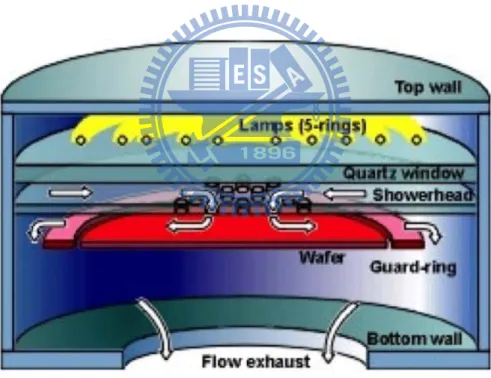
Fig. 3-1 Schematic illustration of the PECVD system………. ……. ……. ……….….48 Fig. 3-2 (a) Schematic illustration of a simple vacuum evaporator, (b) The principle of the electron gun operation……….…..49 Fig. 3-3 Generic RTP reactor: axisymmetric geometry with five independent lamp rings, quartz window and showerhead, and silicon guard ring………. ……. ……...49 Fig. 3-4 Schematics of the ICP high density plasma system.[45] ……. ……. ………….50 Fig. 3-5 (a) RCA clean (b) E-gun →1nm ZrO2 (c) PDA ( w/ or w/o ) →in O2 ambient,
500°C, 5min………...….50 Fig. 3-6 (d) E-gun → 4nm HfO2 (e) PDA→ in O2 ambient, 500°C, 5min……….50
Fig. 3-7 (f) E-gun → 200nm Ti……….51 Fig. 3-8 (a) RCA clean (b) E-gun →1nm ZrO2 (c) PDA ( w/ or w/o ) →in O2 ambient,
500°C, 5min………...….51 Fig. 3-9 (d) E-gun → 4nm HfO2 (e) PDA→ in O2 ambient, 500°C, 5min……….51
Fig. 3-10 (f) Plasma treatment with N2 →200W, 30 and 90sec (g) RTA→ in N2 ambient,
XI
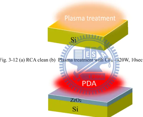
Fig. 3-11(h) E-gun → 200 nm Ti………...52 Fig. 3-12 (a) RCA clean (b) Plasma treatment with CF4 →20W, 10sec………52
Fig. 3-13 (c) E-gun →1nm ZrO2 (d) PDA ( w/ or w/o ) →in O2 ambient, 500°C,
5min……….. ………..52 Fig. 3-14 (e) E-gun → 4nm HfO2 (f) PDA→ in O2 ambient, 500°C, 5min…………...52
Fig. 3-15 (g) E-gun → 200nm Ti….. ………..53 Fig. 3-16 (a) RCA clean (b) Plasma treatment with CF4 →20W, 10sec………53
Fig. 3-17 (c) E-gun →1nm ZrO2 (d) PDA ( w/ or w/o ) →in O2 ambient, 500°C,
5min….. ………..53 Fig. 3-18 (e) E-gun → 4nm HfO2 (f) PDA→ in O2 ambient, 500°C, 5min………..…..53
Fig. 3-19 (g) Plasma treatment with N2, NH3, and N2O →200W, 30 and 90sec……..54
Fig. 3-20 (h) E-gun → 200nm Ti….. ………..54 Fig. 4-1 The comparison of C-V curves of the samples with and without PDA treatment on ZrO2 film in O2 ambient at 500°C for 5 minute………...55
Fig. 4-2 The comparison of C-V curves of the samples with and without PDA treatment on ZrO2 film after CF4 plasma pretreatment. ………...55
Fig. 4-3 The leakage current density comparison of samples with and without PDA treatment. ………56 Fig. 4-4 The leakage current density comparison of samples with and without PDA
treatment after CF4 plasma pretreatment………56
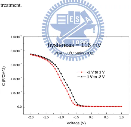
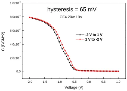
Fig. 4-5 The hysteresis of C-V characteristics was shown for the samples without treatment. ………57 Fig. 4-6 The hysteresis of C-V characteristics was shown for the samples with PDA
treatment. ………57 Fig. 4-7 The hysteresis of C-V characteristics was shown for the samples without PDA treatment after CF4 plasma pretreatment. ………...58
Fig. 4-8 The hysteresis of C-V characteristics was shown for the samples with PDA treatment after CF4 plasma pretreatment. ………...58
Fig. 4-9 The C-V characteristics of samples with various process treatments such as PDA treatment and fluorination treatment. ……….59 Fig. 4-10 The J-V characteristics of samples with various process treatments such as
PDA treatment and fluorination treatment. ……….59 Fig. 4-11 The capacitance-voltage (C-V) characteristics of samples treated in N2 plasma
for 30 sec and 90 sec. ………..60 Fig. 4-12 The J-V characteristics of samples treated by N2 plasma with 30 sec and 90
sec from 0V to -2V are described………60 Fig. 4-13 The hysteresis of C-V characteristics are shown for the samples with 30 sec
N2 plasma treatment………61
Fig. 4-14 The hysteresis of C-V characteristics are shown for the samples with 90 sec
N2 plasma treatment………61
Fig. 4-15 The capacitance-voltage (C-V) characteristics of MIS capacitor treated in N2
plasma for 30 sec and 90 sec with PDA treatment. ………62 Fig. 4-16 The J-V characteristics of MIS capacitor treated in N2 plasma for 30 sec and
90 sec with PDA treatment from 0V to -2V are described………..…62 Fig. 4-17 The hysteresis of C-V characteristics are shown for the samples with PDA
treatment and with 30 sec N2 plasma treatment………..63
Fig. 4-18 The hysteresis of C-V characteristics are shown for the samples with PDA treatment and with 90 sec N2 plasma treatment………..63
Fig. 4-19 The comparison of C-V curves of the samples with and without PDA treatment with 30 sec N2 plasma treatment……….64
Fig. 4-20 The comparison of C-V curves of the samples with and without PDA treatment with 90 sec N2 plasma treatment………...…64
XIII
Fig. 4-21 The leakage current density comparison of samples with and without PDA treatment with 30 sec N2 plasma treatment……….65
Fig. 4-22 The leakage current density comparison of samples with and without PDA treatment with 90 sec N2 plasma treatment……….65
Fig. 4-23 The C-V characteristics of samples with various process treatments such as PDA treatment, fluorination treatment, and nitridation treatment are shown. ……….66 Fig. 4-24 The J-V characteristics of samples with various process treatments such as
PDA treatment, fluorination treatment, and nitridation treatment are shown. ……….66 Fig. 4-25 The capacitance-voltage (C-V) characteristics of MIS capacitor treated in CF4
plasma for 10 sec and N2 plasma for 30 sec and 90 sec..………67
Fig. 4-26 The J-V characteristics of MIS capacitor treated in CF4 plasma for 10 second
and N2 plasma for 30 sec and 90 sec from 0V to -2V are described……...…67
Fig. 4-27 The hysteresis of C-V characteristics are shown for the samples with fluorination and with 30 sec N2 plasma treatment……….…68
Fig. 4-28 The hysteresis of C-V characteristics are shown for the samples with fluorination and with 90 sec N2 plasma treatment……….…68
Fig. 4-29 The capacitance-voltage (C-V) characteristics of MIS capacitor treated in CF4
plasma for 10 sec and N2 plasma for 30 sec and 90 sec with PDA
treatment. ………69 Fig. 4-30 The J-V characteristics of MIS capacitor treated in CF4 plasma for 10 sec and
N2 plasma for 30 sec and 90 sec with PDA treatment from 0V to -2V are
described. ………69 Fig. 4-31 The hysteresis of C-V characteristics are shown for the samples with
Fig. 4-32 The hysteresis of C-V characteristics are shown for the samples with fluorination, PDA treatment, and with 30 sec N2 plasma treatment……..…70
Fig. 4-33 The comparison of C-V curves of the samples with and without PDA treatment on ZrO2 film with fluorination and 30 sec N2 plasma
treatment. ………..71 Fig. 4-34 The comparison of C-V curves of the samples with and without PDA
treatment on ZrO2 film with fluorination and 90 sec N2 plasma
treatment………71 Fig. 4-35 The comparison of J-V curves of the samples with and without PDA treatment on ZrO2 film with fluorination and 30 sec N2 plasma treatment…………...72
Fig. 4-36 The comparison of J-V curves of the samples with and without PDA treatment on ZrO2 film with fluorination and 90 sec N2 plasma treatment. …………...72
Fig. 4-37 The C-V characteristics of samples with various process treatments such as PDA treatment, fluorination treatment, and nitridation treatment. ………….73 Fig. 4-38 The J-V characteristics of samples with various process treatments such as
PDA treatment, fluorination treatment, and nitridation treatment. ………….73 Fig. 4-39 The capacitance-voltage (C-V) characteristics of MIS capacitor treated in CF4
plasma for 10 sec and N2O plasma for 30 sec and 90 sec. ……….74
Fig. 4-40 The J-V characteristics of MIS capacitor treated in CF4 plasma for 10 second
and N2O plasma for 30 sec and 90 sec from 0V to -2V are described. ……..74
Fig. 4-41 The hysteresis of C-V characteristics are shown for the samples with fluorination and with 30 sec N2O plasma treatment………..75
Fig. 4-42 The hysteresis of C-V characteristics are shown for the samples with fluorination and with 90 sec N2O plasma treatment………..75
Fig. 4-43 The capacitance-voltage (C-V) characteristics of MIS capacitor treated in CF4
XV
treatment. ………76 Fig. 4-44 The J-V characteristics of MIS capacitor treated in CF4 plasma for 10 sec and
N2O plasma for 30 sec and 90 sec with PDA treatment from 0V to -2V are
described. ………76 Fig. 4-45 The hysteresis of C-V characteristics are shown for the samples with
fluorination, PDA treatment, and with 30 sec N2O plasma treatment……..77
Fig. 4-46 The hysteresis of C-V characteristics are shown for the samples with fluorination, PDA treatment, and with 90 sec N2O plasma treatment……...77
Fig. 4-47 The comparison of C-V curves of the samples with and without PDA treatment on ZrO2 film with fluorination and with 30 sec N2O plasma
treatment………78 Fig. 4-48 The comparison of C-V curves of the samples with and without PDA
treatment on ZrO2 film with fluorination and with 90 sec N2O plasma
treatment………78 Fig. 4-49 The comparison of J-V curves of the samples with and without PDA treatment on ZrO2 film with fluorination and with 30 sec N2O plasma treatment…….79
Fig. 4-50 The comparison of C-V curves of the samples with and without PDA treatment on ZrO2 film with fluorination and with 90 sec N2O plasma
treatment………79 Fig. 4-51 The C-V characteristics of samples with various process treatments such as PDA treatment, fluorination treatment, and nitridation treatment are shown. ……….80 Fig. 4-52 The J-V characteristics of samples with various process treatments such as PDA treatment, fluorination treatment, and nitridation treatment are shown. ……….80 Fig. 4-53 The capacitance-voltage (C-V) characteristics of MIS capacitor treated in CF4
plasma for 10 sec and NH3 plasma for 30 sec and 90 sec. ……….81
Fig. 4-54 The J-V characteristics of MIS capacitor treated in CF4 plasma for 10 second
and NH3 plasma for 30 sec and 90 sec from 0V to -2V are described………81
Fig. 4-55 The hysteresis of C-V characteristics are shown for the samples with fluorination and with 30 sec NH3 plasma treatment………..82
Fig. 4-56 The hysteresis of C-V characteristics are shown for the samples with fluorination and with 90 sec NH3 plasma treatment………..82
Fig. 4-57 The capacitance-voltage (C-V) characteristics of MIS capacitor treated in CF4
plasma for 10 sec and NH3 plasma for 30 sec and 90 sec with PDA
treatment. ………83 Fig. 4-58 The J-V characteristics of MIS capacitor treated in CF4 plasma for 10 sec and
NH3 plasma for 30 sec and 90 sec with PDA treatment from 0V to -2V are
described. ………83 Fig. 4-59 The hysteresis of C-V characteristics are shown for the samples with
fluorination, PDA treatment, and with 30 sec NH3 plasma treatment……...84
Fig. 4-60 The hysteresis of C-V characteristics are shown for the samples with fluorination, PDA treatment, and with 90 sec NH3 plasma treatment. …….84
Fig. 4-61 The comparison of C-V curves of the samples with and without PDA treatment on ZrO2 film with fluorination and 30 sec NH3 plasma treatment
are shown. ……….. ………..……85 Fig. 4-62 The comparison of C-V curves of the samples with and without PDA
treatment on ZrO2 film with fluorination and 90 sec NH3 plasma treatment
are shown. ……….85 Fig. 4-63 The comparison of J-V curves of the samples with and without PDA treatment on ZrO2 film with fluorination and 30 sec NH3 plasma treatment are
XVII
Fig. 4-64 The comparison of J-V curves of the samples with and without PDA treatment on ZrO2 film with fluorination and 90 sec NH3 plasma treatment are
shown. ……….86 Fig. 4-65 The C-V characteristics of samples with various process treatments such as PDA treatment, fluorination treatment, and nitridation treatment are shown. ……….87 Fig. 4-66 The J-V characteristics of samples with various process treatments such as
PDA treatment, fluorination treatment, and nitridation treatment are shown. ……….87 Fig. 4-67 The capacitance-voltage (C-V) characteristics of MIS capacitors combined
CF4 plasma treatment with N2, NH3, or N2O plasma treatment at optimal
condition are shown. ………...88 Fig. 4-68 The J-V characteristics of MIS capacitors combined CF4 plasma treatment
with N2, NH3, or N2O plasma treatment at optimal condition are shown…...88
Chapter 1
Introduction
1.1 Background
The semiconductor device has a fairly long history, since that first IC (integrated circuit), circuit design has become more sophisticated, and the integrated circuit more complex. MOS transistors can be made quite small, occupying a small silicon area on IC chip, and their manufacturing process is relatively simple, compared with bipolar junction transistor (BJT) manufacturing process. Furthermore, digital logic and memory functions can be implemented with circuits that use MOSFETs only (that is, no resistors or diodes are needed). This is the reason why most very-large-scale integrated (VLSI) circuits are made at the present time using complementary metal-oxide-semiconductor (CMOS) technology, including microprocessor and memory chips. CMOS technology has also been applied extensively in the design of analog integrated circuits and in integrated circuits that combine both analog and digital circuits. Since the 1980s, devices have been scaled such that performance doubled as the cost was cut in half every 2-5 years. This is the famous “Moore’s law”.
According to the recent prediction which was made by the Semiconductor Industry Association (SIA) in International Technology Roadmap for Semiconductors (ITRS) [1-3], the IC technology will continue its historical rate of advancement with Moore’s law for at least a couple of decades. ”Moore’s Law”, proposed by Gordon Moore in 1965, which states that “ The number of transistors and resistors on a chip doubles every 18 months ”, so it is needed to pursue better performance with lower cost. As the scaling rule keeps going, the dimension of gate oxide for complementary metal oxide semiconductor (CMOS) has decreased dramatically for the past decade. For more than 30 years, SiO2 films have been the preferred material for gate dielectric in
2
MOS-based structures. A traditional Si-based MOS structure is obtained by growing a layer of silicon dioxide (SiO2) on top of silicon substrate and depositing a layer of metal
or polycrystalline silicon. Silicon dioxide is a good candidate for gate because it has many advantages in IC technology. For example, it has good stability, high-quality Si/ SiO2 interface, and outstanding isolation properties. SiO2 is an almost perfect insulator
with a resistivity in excess of 1016Ωcm. The insulating films of SiO2 grown on silicon
are smooth and coherent with no holes in a thickness range down to single atomic layers. The interface with silicon is abrupt and there are very few electrically active defects at the interface.
However, as the conventional gate dielectric scales down to 1.0 nm~1.5 nm, the viability of SiO2 will face several challenges like a large leakage current occurs through
the ultra-thin oxide by direct tunneling mechanism [4].This phenomenon increases standby power consumption and loss of inversion charge which degrade the reliability and performance of device seriously. In order to suppress the leakage current and maintain excellent performance of device, replace the conventional SiO2-based
dielectric by high-k dielectric as a gate insulator is necessary. Using the material with high dielectric constant (high-k), the physical thickness of the dielectric in the devices can be increased without the reduction of capacitance density. Since the leakage current is related to the physical thickness, the increasing thickness of high-k dielectric can reduce the leakage current of the devices. Although high-k dielectrics often exhibits smaller band gap, weaker bond, and higher defect density than SiO2, the high-k
dielectrics with the same effective oxide thickness (EOT) with SiO2 still shows lower
leakage current than SiO2 by several orders. [5-6] That is the reason why high-k
dielectrics have drawn much attention for future gate dielectrics.
Although reduced leakage current density has been observed in some devices with high-k gate dielectrics, there are still several problems to be solved, including
thermal stability, interface quality between high-k gate dielectrics and Si-substrate, mobility degradation, reliability, charge trapping, and fabrication integrity with IC technology.
1.2 Scaling down of gate dielectric thickness
For the improvement of the performance and circuit density of CMOS, scaling down gate length and insulator layer thickness is a trend for silicon process.
The most important parameter is the current between source and drain (Id) which the device could be driven.
I
dsat =μC
oxWL
(V
G-V
T)
2
(1.1)
μ is the channel carrier mobility, Cox is the capacitance if gate oxide dielectric, W
is the width of the transistor channel, L is the length of the transistor channel, VG is the
gate-to-source applied voltage, VT is the threshold voltage. From the formula, we know
that with reduced threshold voltage, smaller effective channel length, and increased gate capacitance as well as gate-to-source voltage, the device can achieve better current driving ability. Of course, it can also have higher device density, which means a better performance and much more transistors on the chip.
As shown in Fig. 1-1 [7] and Fig. 1-2 [8], according to the International Technology Roadmap for Semiconductors (ITRS), the equivalent oxide thickness (EOT) of gate dielectric should be less than 1.0 nm for 65 nm technology node. The gate direct tunneling leakage current through the SiO2 was so high (above 1 A-cm-1 at 1.5 nm) that
power dissipation increased to undesirable values [9-11]. In order to solve the problem of gate leakage current of SiO2, It was essential to replace SiO2 as a gate oxide dielectric.
4
I
dsat=C
gμ
n W L(V
GS-V
T)
2(1.2)
C
g = kε0A
(1.3)
From (1.2)(1.3) the direct way to reduce the leakage current is to make the oxide thickness thicker, which can repress the direct tunneling current. High-k gate materials can maintain the same EOT with thicker physical thickness, and is therefore expected drastically reduced direct-tunneling current. From Fig. 1-3, the increased physical thickness significant reduces the probability of tunneling across the insulator, and hence, reduces the amount of off-state leakage current density. [12]
Although reduced leakage current density has been observed in some devices with high-k gate dielectrics, there are still several problems to be solved, including thermal stability, interface quality between high-k gate dielectrics and Si-substrate, mobility degradation, reliability, charge trapping, and fabrication integrity with IC technology.
1.3 The problem of poly-silicon as the gate electrode
The traditional poly-silicon gate electrode would face two major problems due to shrink the channel length (1) Under Continuing to shrink the gate oxide layer in the p-MOSFET, boron within the p-type poly-Si gate electrode would penetrate the gate oxide with doping process or subsequent annealing process, resulting in the initial offset voltage [13-14] as well as reducing the reliability of the gate oxide; (2) After the gate voltage was applied, since poly-silicon was the same as the characteristics of the semiconductor silicon substrate, it would produce depletion effect which was called poly-depletion [15-16]. Thereby the capacitance value of the gate oxide and carriers in the channel would decrease, affecting the operation of the CMOS device.
phonon scattering in the high-k gate dielectric from coupling to the channel under inversion conditions, resulting in improved channel electron mobility [17-18]. Recently, metal-gate/high-k gate dielectric process technologies became one of the most important researches in the semiconductor industry.
1.4 The choice of High-k materials
Table 1-1 illustrates Material requirement of high-k dielectrics. For most high-k materials, the higher dielectric constant comes at the expense of narrow band gap. The lower barrier height for tunneling current tends to compensate the benefit of the higher dielectric constant. Even though there are many materials with significantly high-k values, many of them are not suitable for gate dielectric applications since they do not satisfy all of these necessary conditions.
An ideal gate dielectric should meet the following requirements below:
Physical properties :
a. Suitable high k value (12~60)
A suitable k value is indispensable. Those with not enough high-k value could not satisfy to lower the leakage by increasing physical thickness. The k value tended to vary inversely with the band gap, a very large k was undesirable in CMOS design because they caused undesirable large fringing fields at the source and drain electrodes. So we chose the k value within 25 to 30 which satisfied the requirement of leakage current. b. Wide bandgap with conduction band offset > 1eV
It is found that most of the high-k materials do not have wide enough bandgap. In contact with silicon and gate electrode, the bandgap is closely related to the barrier height for carrier transport. Low bandgap will lead to intolerably high gate leakage (leakage current ~exp(-△ Ec)). The high-k gate dielectrics that satisfied this criterion were ZrO2, HfO2, Al2O3, Y2O3, La2O3 and various lanthanides and their silicates and
6
aluminates.
c. Thermodynamic stability in direct contact with silicon
Direct growth of high-k gate dielectric on silicon substrate was usually accompanied by extensive inter-diffusion or chemical reactions that degrade the properties of the gate dielectric, the underlying silicon, or both [19]. The high-k gate dielectric must not react with Si to form either SiO2 or a silicide due to the resulting
SiO2 layer would increase the EOT and the silicide was metallic and would short out the
field effect.
d. Film morphology (amorphous) and stable process compatibility
In the VLSI process, the thermal budget is an important issue since high temperature changes dielectric phase. Once the gate dielectric material has transformed to polycrystalline from amorphous phase, the large grain boundaries would serve as leakage path, and induce large leakage current.
e. Gate material compatibility
Materials such as metal gate, and metals have been considered for better controllability and better performance.
Electrical properties :
(a) Low interface state density (Dit< 5x10¹⁰/cm2-eV-1), and SiO2-like mobility.
The carriers in the channel flowed within the gate dielectric /Si substrate interface. Hence, this interface must be of the highest electrical quality, in terms of less roughness and the absence of interface defects. In high-k, there are so many sources that would reduce mobility, such as fixed charge, remote phonon, interfacial dipoles, remote surface roughness, surface roughness and phase separation crystallization.
(b) Tinv<1nm.
(c) J<10-3A/cm2@ VDD. (d) VFB and hysteresis < 20mV.
(e) No C-V dispersion. (f) Reliability issue.
We must also take the electrical reliabilities into account. For example, hysteresis, hot-carrier stress (HCS), constant voltage stress (CVS), stress-induced leakage current (SILC), time dependent dielectric breakdown (TDDB), positive bias temperature instability (PBTI), negative bias temperature instability (NBTI) and the charge trapping problem.
1.5 Why choose ZrO
2and HfO
2The high-k gate dielectric must not react with Si to form either SiO2 or a silicide
due to the resulting SiO2 layer would increase the EOT and the silicide was metallic and
would short out the field effect. Thus, the suitable high-k gate dielectrics left us ZrO2,
HfO2, Al2O3, Y2O3, La2O3, Sc2O3 and some lanthanides such as Pr2O3, Gd2O3 and
Lu2O3. Unfortunately, many high-k materials such as SrTiO3, TiO2, Ta2O5 and
BaSrTiO3 are thermally unstable when directly contacted with silicon [20] and need an
additional barrier layer which may add process complexity and impose thickness scaling limit. Also, materials with too low or too high dielectric constant may not be adequate choice for alternative gate dielectric application.
Among the medium-k materials compatible with silicon, oxides of Zr and Hf are attracting much attention recently. Especially, Hf forms the most stable oxide with the highest heat of formation(△Hf=271Kcal/mol) the periodic table (i.e. Ti, Zr, Hf). Unlike other silicides, the silicide of Hf can be easily oxidized [21]. From the requirements of high-k gate dielectric which had mentioned previously, ZrO2, HfO2, Al2O3, Y2O3, La2O3
were the desirable candidates using for high-k gate dielectric. La2O3 had a slightly
higher k than HfO2 but was more hygroscopic. Table 1-2 shows that some important
8
rather low k value. Y2O3 had lower k value than HfO2 and poor thermal stability due to
heavily reactive with Si. Thus, ZrO2 and HfO2 are both generally believed to be two
good materials for high-k gate dielectric. However, it was found that ZrO2 was slightly
reactive with Si and can form ZrSi4. For this reason, HfO2 was presently the preferred
high-k gate dielectric over ZrO2. Table 1-3 shows that several properties of HfO2 and
ZrO2. HfO2 is very resistive to impurity diffusion and intermixing at the interface
because of its high density (9.68 g/cm3) [23]. In addition, HfO2 is the first high-k
material showing compatibility with polysilicon gate process [24]. Therefore, among the high-k dielectrics being studied , HfO2 appears promising due to its relatively high
dielectric constant (~25) as compared to Si3N4 and Al2O3 [25], its relatively high free
energy of reaction with Si (47.6Kcal/mole at 727°C) as compared to TiO2 and Ta2O5
[26], and its relatively large bandgap (~5.8eV) [27]. These properties make HfO2 to be
one of the most promising candidates for alternative gate dielectric application.
1.6 Challenges of high-k material
Although high-k material is expected to replace SiO2 ideally, there are many
problems to use high-k material practically. The issues for choosing a high-k material may include:
(1) Low dielectric constant interfacial layer between substrate and high-k material (2) Degradation of carrier mobility
(3) Shift of threshold voltage (4) Thermal stability
(5) Boron penetration prevention
(6) Poly interface and poly gate electrode
1.7 Current conduction mechanisms
The current conduction mechanisms identified in Hf-based gate dielectrics are generally attributed to a Schottky emission (SE), the Frenkel-Poole (FP) emission, or Fowler-Nordheim (FN) tunneling. The schematic of the current conduction mechanism in gate oxide band states is shown in Fig. 1-4.
1.7.1 Schottky Emission (SE)
The thermionic emission models range in various levels of physical complexity. The J–E relation for Schottky emission (SE) was given by the Schottky-Richardson relation as [28]
J
SEAT exp
βSE√E KT(1.4)
where βSE is given byβ
SE πε ε(1.5)
AndA
C
RDexp
B KT(1.6)
where ε is the dynamic dielectric constant, ε is the permittivity of the free space, k is the Boltzmann constant, T is the absolute temperature.CRD is the Richardson constant,
and qφB is the barrier height.
1.7.2 Frenkel-Poole (FP) emission
The Poole–Frenkel (PF) effect was due to the thermal excitation of charge carriers from Coulombic traps in the bulk of a dielectric or semiconductor, enhanced by the application of an electric field.
10
J
C Eexp
φB β√EξKT
(1.7)
And β is given by
β
πε ε(1.8)
where Ct is a trap density related constant and qφB is the ionization potential in eV,
which is the energy required for the trapped electron to escape the influence of the positive nucleus of the trapping center when no field is applied. β√E is the trap barrier height reduced by the applied electric field E. ξ is the factor and vary between 1 and 2, ε is the dynamic dielectric constant and ε is the permittivity of the free space.
1.7.3 Fowler-Nordheim (FN) tunneling
According to the FN model, the current density which flowed through a thin dielectric layer when an electric field E was applied reads [29] :
J
AE exp
B E(1.9)
whereB
√(2.0)
andA
π φ(2.1)
where m is the electron mass, m* is the effective electron mass in the gate oxide, h the Planck’s constant and qφ is the cathode barrier height.
1.8 Thesis organization
In this thesis, following chapters were primarily organized :
In chapter 2, we indicated our motivation for using plasma fluorination and plasma nitridation.
In chapter 3, we described the details of our experiment. Dual electron gun evaporation system was used to deposit ZrO2/HfO2 stack dielectric and
plasma-enhanced chemical vapor deposition (PECVD) system was used to plasma fluorination and high-density plasma source of HDPCVD was used to plasma nitridation.
In chapter 4, we discuss the electrical characteristics of ZrO2/HfO2 stack insulator
by Metal Insulator Semiconductor (MIS) capacitors.
In chapter 5, we make the conclusions for this thesis and provide some suggestions for future work.
12
Chapter 2
Motivation
2.1 Plasma fluorination
The MOS devices have properties with the result that there is often Nit or Dit in
the interface, imperfect bonding of interface usually makes the characteristic of the device deteriorate. For example, charge will be trapped by the defects of the interface, it produces flat band voltage shift and also reduces the carrier mobility. Another shortcoming is that these dangling bonds will easily bond with oxygen atoms in the following high temperature environment. The extra chemical reaction will let the interfacial oxide growth, and it will reduce the C value because of the lower dielectric constant.In addition, the quality of interfacial layer formed by oxidation is worse and there still will be the more problems of charge trapping.
HfO2 was a good gate dielectric due to its high dielectric constant [30-35], wide
energy bandgap (~5.68 eV), and high stability with the Si surface. Unfortunately, they suffered from a high density of charge traps which caused flat-band voltage shift, threshold voltage instability, Coulombic scattering of carriers in the channel and hysteresis problems [36].
On the other hand, the unavoidable formation of interfacial layer (IL) was another critical issue, limiting the reduction of the effective oxide thickness. The reasons for this unwanted layer were the presence of excess oxygen during the film growth that initially oxidized the Si surface and Si diffusion into the film producing a silicate layer [37]. Because the quality of interfacial layer formed by oxidation was worse, it caused the problem of charge trapping. Plasma fluorination and plasma nitridation were considered to be effective methods for melioration of properties of HfO2 gate dielectric.
performance [36-40]: (a) Fluorine was believed to form stronger Hf–F and Si–F bonds than Hf–H and Si–H bonds, leading to improvement of the reliability of HfO2/SiO2, (b)
The interfacial layer (IL) between HfO2 film and Si substrate could effectively be
suppressed by a pre-deposition CF4 plasma treatment, (c) The charge trapping effect
could greatly be eliminated for the HfO2 gate dielectric by the post-deposition CF4
plasma treatment, (d) The thermal stability of HfO2 gate dielectric could be much
improved by fluorine ion implantation on the silicon surface.
An inner-interface trapping model was presented to explain the hysteresis [39], as shown in Fig. 2-1. It shows that the voltage was swept from accumulation to inversion, the C-V curve shifted negatively, in contrary to the C-V curve shifted positively when the voltage was swept from inversion to accumulation. The positive and negative carrier trappings caused the C-V curve to have a hysteresis loop. After CF4 plasma treatment,
Fluorine passivated the dangling bond and accumulated at the interfacial layer, as shown in Fig. 2-2. It appeared that fluorine incorporation improved the interface quality and resulted in less hysteresis.
2.2 Plasma nitridation
Nitridation was also a common method to improve the properties of HfO2 gate
dielectric. Nitrogen incorporation into Hf-based high-k dielectrics has been intensively studied.According to traditional view of improving SiO2 device performance, we could
find that nitridation is a common method to improve the interface [41]. Property with the result that there is often Nit or Dit in the interface, imperfect bonding of interface
usually makes the characteristic of the device deteriorate.
In order to solve these problems, nitridation treatment could let the atom of nitrogen bond with these dangling bonds and fix it while entering the interface layer, and then improve the stability and reliability of interface.
14
The driving force of this reaction is total energy stabilization with charge compensation. In this charge compensation, charge transfer arises from two electrons of the induced Vo gap state falling into the two vacant N states at the top of the valence
band as shown in Fig. 2-3. As a result, a large amount of N induces a large amount of Vo. The key point is the increase in Vo–Vo interactions with the increase in the amount
of Vo. A large amount of N induces the deterioration of the CB offset owing to Vo–Vo
interaction as shown in Fig. 2-4 [42]. If we use N doped HfO2, the deterioration of the
VB offset is inevitable. If Vo can move easily, total energy is stabilized by local
crystallization around Vo owing to disturbance by the movement of Vo, because the
crystal state is lower in energy than the amorphous state. A pair of Fs and Ns can
passivate the Vo with no excess charges as shown in Fig. 2-5. The main passivation
energy comes from one excess electron transfer of CB bottom of Fs to VB top of Ns as
shown in Fig. 2-5. The amount of N is not needed large, because Fs fills up Vo.
Moreover, CB lowering owing to Vo–Vo interaction can be avoided. Defects formation
in HfO2 should be affected \by its crystal structure. But the fact that the CB of HfO2 is
composed of Hf 5d states, and the VB is composed of O 2p states is not affected by its crystal structure. The stabilization mechanism by the electron transfer is not affected by its crystal structure. That is to say, fluorines can fill up oxygen vacancies in HfO2 by
exothermic reaction, but induce distribution of the positive charges in HfO2 [43]. The
most important point is that we should fill up Vo by fluorine (Fs), and Fs donates an
excess electron to other acceptor type dopant. This passivation process completely eliminates Vo with no excess charges in gate oxide. The amount of N is not needed large,
because Fs fills up all oxygen vacancies [43]. According to [44], we could understand
that the effect of plasma nitridation is better than thermal nitridation. The reason is that high-k materials could not sustain high thermal stress. As long as the temperature reaches certain degree, we would see the phenomenon of crystallization. The
crystallization of dielectric would increase leakage current substantially, because it offers the path of leakage current. On the other hand, the meaning of plasma nitridation is to activate the source gas first. The high activation energy of radical will provide better mend which is better than nitridation at high temperature. For all these reasons, we adopt plasma nitridation in present experience.
2.3 Dual plasma treatment
In this thesis, we tended to employ CF4 plasma for pre-deposition of ZrO2
treatment in order to eliminate the low dielectric constant interfacial layer and improved the quality of silicon substrate surface. In the next step, we used the NH3, N2O and N2
plasma for post-deposition of HfO2 treatment because of the capability of nitrogen
incorporated HfO2 gate dielectric to reduce oxygen vacancies and increase the
crystallization temperature of HfO2.
The method that combined pre-deposition plasma fluorination and post-deposition plasma nitridation was called dual plasma treatment.
16
Chapter 3
Experimental of Ti/HfO
2/ZrO
2/Si MIS capacitors
3.1 PECVD system for plasma treatment
Plasma-enhanced chemical vapor deposition (PECVD) is a process used to deposit thin films on a substrate. After creation of the plasma of the reacting gases, chemical reactions are induced into the process. The plasma is generally created by AC (RF) frequency or DC glow discharge between two electrodes. The chamber space between two electrodes is filled with the reacting gases.
Plasma is any neutral gas which is partially ionized and contains the positive charges (ions), negative charges (electrons) and neutral particles. Density of the charged particles is high enough to produce Coulomb interaction. This phenomenon induces the charged particles to reveal behaviors of fluid, resulting in the properties of the plasma.
In generally, the plasma is at neutral state, that is, the density of negative charged particles and the density of positively charged particles are the same. When some particles undergo external force, other particles will be affected. Thus the plasma has a good electrical conductivity and thermal conductivity.
Plasma is generated by electrons which are accelerated by electric field to very high kinetic energy and then impact with gas atoms or molecules to produce ionic reaction. The gas atoms or molecules which are impacted by electrons dissociate as a positive charged ion and an electron. The results of this dissociation will produce two free electrons, they will be accelerated again and the impact of other gas molecules or atoms so that it can produce four free electrons. By the continuous reaction, gases within the zone of reactive chamber are ionized.
Plasma treatment had two advantages which were different from the traditional thermal ones :
(1) When using plasma process for the chemical reactions, electrons impacted the gas molecules and produced the high reactive species, leading to the reactions which occur difficultly in the thermodynamics could be generated.
(2) Traditional thermal chemical reactions usually needed high thermal energy to control the conditions of reaction. Therefore the high temperature was required but this was not what we want due to the high-k materials could not sustain high thermal stress. Plasma process could effectively induce chemical reactions without high temperature, so we tended to use plasma fluorination.
We used the SAMCOs PD-220N PECVD system for our plasma treatment. Fig. 3-1 shows the Schematic illustration of the PECVD system. This is a diode-type plasma system. The process gas and carrier gas (inert gas) flowed into chamber. Here we used CF4 as the process gases. RF power source was applied at the top electrode and the
bottom electrode connects to ground. The process gases got energy from the RF power source and then generated the plasma. Wafer was placed on the bottom electrode and the charged particles within plasma accelerated toward to the bottom electrode due to potential difference between top electrode and bottom electrode. Thus plasma fluorination was completed during the plasma process.
3.2 Electron beam evaporation system
Fig. 3-2(a) shows a schematic illustration of a simple vacuum evaporator. It is mainly constituted by an evaporator chamber and a vacuum system which provides the required degree of vacuum. In the evaporator chamber, the solid materials used to deposit are called evaporation sources. They will be placed in the crucible manufactured from refractory. The crucible constituted by the conductive materials connects directly to DC power outside the chamber. When appropriate current flowing into the crucible, heat generated due to the resistance effect of the crucible. Source placed inside the
18
crucible will be heated until it is close to the melting point. At this time, solid sources will evaporate and become vapor. Therefore, we can deposit thin film which we want onto the wafer.
In general, electron beam evaporation (EBE) system was popular for the applications of semiconductor industry. The basic structure is the same as Fig. 3-2 (a). The major distinction is that EBE system heats the evaporation source by electron beam, as shown in Fig. 3-2 (b).
3.2.1 Dual electron gun evaporation system
A Dual electron gun evaporation system is used for electron beam evaporations. This system provides the capability for the evaporation of high melting point materials. The source has two crucibles, which enable multiple evaporations to be performed. The electron beam gun (e-gun) is within a high vacuum chamber.
3.3 Rapid thermal annealing (RTA) system
Metal RTA-AG610 is a single-wafer lamp-heated and computer-controlled rapid thermal processing (RTP) system. Generic RTP reactor is shown in Fig. 3-3. Water and compressed dry air (CDA) cooling system are used to cool down the quartz chamber. High intensity visible radiation heating and cold-heating chamber walls allow fast wafer heating and cooling rate. The tungsten halogen lamps are distinguished into five groups, and the relative percentage of lamp intensity can be adjusted individually for each group to achieve uniform temperature distribution. Temperature is obtained from pyrometer and precise controlled by computer. Two gas lines are used in the system which can be switched between Ar and N2. Before RTA process starts, one
minute N2 gas purge is performed to minimize the water vapor introduced during wafer
loading and also sweep unwanted particles induced during process. A fast heating rate of 150oC/s was chosen in this work. When anneal was complete, chamber temperature
was quickly cooled down from 600oC to 400oC by 30 seconds N2 purge. Then, the
chamber was slowly cooled down to 300oC without N2 purge to avoid creaking of films.
After five minutes later, wafers were taken out from the chamber. Films’ creak could be avoided by two-steps-cooling method.
3.4 Inductively coupled plasma (ICP) system
The high-density plasma source of HDPCVD is come from inductively coupled plasma(ICP) system. The inductive coils shown in Fig. 3-4[45] serve just like the initial coils of a transformer. When an RF current flows in the coils, it generates a changing magnetic field. The inductively coupled electric field accelerates electrons and causes ionization collisions. Since the electric field is in the angular direction, electrons are accelerated in the angular direction, which allows electrons to travel a long distance without collisions with the chamber wall or electrode.[46] 13.56 MHz RF power was coupled to the top electrode through a matching network. After the sample load to reactor, the system was pumped down to keep the chamber clean enough. Subsequently, the source gas was become radical by the plasma system, as the chamber pressure was 100 mTorr and the substrate temperature was 300°C so that to achieve the goal of low temperature process. The power of working plasma was kept constant at 200W and the flow rate of source gas was 100 sccm. While the process of plasma treatment was finished, these samples were brought to thermal treatment to reduce plasma damage.
3.5 Experiment Details
3.5.1 Post deposition annealing (PDA) effect on ZrO
2MIS capacitors with Ti/HfO2/ZrO2/Si structure was fabricated on (100) oriented
p-type silicon wafers which were one side polished and their resistivity was 0.1 to 1 ohm-cm. Fig. 3-5, Fig. 3-6, and Fig.3-7 shows that flowchart of fabrication of MIS capacitors in our experiment.
20
Prior to the growth of HfO2/ZrO2 stack dielectrics, the native oxide was cleaned
by the conventional RCA cleaning and diluted HF etching in sequence for the removal of particles and native oxides. After standard initial RCA clean, a 1nm ZrO2 thin film
was grown on Si substrate by Dual E-gun evaporate deposition system. After that, some samples were subjected to post deposition annealing (PDA) treatment in O2 ambient at
500°C for 5 minute, and the others without PDA. Then, a 4nm HfO2 thin film was
grown on Si substrate by Dual E-gun evaporate deposition system. After the thin films were deposited, all samples were annealed in O2 ambient for 5 minute at 500°C after
deposition (PDA, Post deposition anneal) again.
Finally, all samples were deposited 200nm thick Ti layer defined as shadow mask by E-gun. The active region pad of etch capacitors’area was 1.33×10⁻⁴/cm 2.
3.5.2 Plasma treatment on HK
stack w/ or w/o ZrO
2PDA
MIS capacitors with Ti/HfO2/ZrO2/Si structure was fabricated on (100) oriented
p-type silicon wafers which were one side polished and their resistivity was 0.1 to 1 ohm-cm. Fig. 3-8, Fig. 3-9, Fig. 3-10 and Fig. 3-11 shows that flowchart of fabrication of MIS capacitors in our experiment.
Prior to the growth of HfO2/ZrO2 stack dielectrics, the native oxide was cleaned
by the conventional RCA cleaning and diluted HF etching in sequence for the removal of particles and native oxides. After standard initial RCA clean, a 1nm ZrO2 thin film
was grown on Si substrate by Dual E-gun evaporate deposition system. After that, some samples were subjected to post deposition annealing (PDA) treatment in O2 ambient at
500°C for 5 minute, and the others without PDA. Then, a 4nm HfO2 thin film was
grown on Si substrate by Dual E-gun evaporate deposition system. After the thin films were deposited, all samples were annealed in O2 ambient for 5 minute at 500°C after
The next step was using HDPCVD to add plasma N2 treatment in order to
improve the electrical properties of dielectric. The deposition source N2 flow rate was
100 sccm, ICP power was 200 W, bias was 0 W, process pressure was 100 mTorr, and process time was 30 sec and 90 sec, temperature was 300°C. After nitridation, we also annealed these samples to reduce the plasma damage (PNA, Post nitridation anneal).
Finally, all samples were deposited 200nm thick Ti layer defined as shadow mask by E-gun. The active region pad of etch capacitors’area was 1.33×10⁻⁴/cm 2 .
3.5.3 Post deposition annealing (PDA) effect on ZrO
2after
plasma fluorination pretreatment
MIS capacitors with Ti/HfO2/ZrO2/Si structure was fabricated on (100) oriented
p-type silicon wafers which were one side polished and their resistivity was 0.1 to 1 ohm-cm. Fig. 3-12, Fig. 3-13, Fig. 3-14, and Fig. 3-15 shows that flowchart of fabrication of MIS capacitors in our experiment.
Prior to the growth of HfO2/ZrO2 stack dielectrics, the native oxide was cleaned
by the conventional RCA cleaning and diluted HF etching in sequence for the removal of particles and native oxides. After standard initial RCA clean, wafers are placed into the chamber of PECVD. All samples were prepared in CF4 plasma. The reactive
pressure and flow rate of CF4 was 67 Pa and 100 sccm, respectively. The substrate
temperature was increased to 300oC and the RF power was 20 W for CF4 plasma
exposure times of 10 seconds.
After CF4 plasma pre-deposition treatment, a 1nm ZrO2 thin film was grown on
Si substrate by Dual E-gun evaporate deposition system. After that, some samples were subjected to post deposition annealing (PDA) treatment in O2 ambient at 500°C for 5
minute, and the others without PDA. Then, a 4nm HfO2 thin film was grown on Si
22
deposited, all samples were annealed in O2 ambient for 5 minute at 500°C after
deposition (PDA, Post deposition anneal) again.
Finally, all samples were deposited 200nm thick Ti layer defined as shadow mask by E-gun. The active region pad of etch capacitors’area was 1.33×10⁻⁴/cm 2.
3.5.4 Plasma treatment on HK
stack w/ or w/o ZrO
2PDA
after plasma fluorination pretreatment
MIS capacitors with Ti/HfO2/ZrO2/Si structure was fabricated on (100) oriented
p-type silicon wafers which were one side polished and their resistivity was 0.1 to 1 ohm-cm. Fig. 3-16, Fig. 3-17, Fig. 3-18, Fig. 3-19 and Fig. 3-20 shows that flowchart of fabrication of MIS capacitors in our experiment.
Prior to the growth of HfO2/ZrO2 stack dielectrics, the native oxide was cleaned
by the conventional RCA cleaning and diluted HF etching in sequence for the removal of particles and native oxides. After standard initial RCA clean, wafers are placed into the chamber of PECVD. All samples were prepared in CF4 plasma. The reactive
pressure and flow rate of CF4 was 67 Pa and 100 sccm, respectively. The substrate
temperature was increased to 300oC and the RF power was 20 W for CF4 plasma
exposure times of 10 seconds.
After CF4 plasma pre-deposition treatment, a 10Å ZrO2 thin film was grown on Si
substrate by Dual E-gun evaporate deposition system. After that, some samples were subjected to post deposition annealing (PDA) treatment in O2 ambient at 500°C for 5
minute, and the others without PDA. Then, a 40Å HfO2 thin film was grown on Si
substrate by Dual E-gun evaporate deposition system. After the thin films were deposited, all samples were annealed in O2 ambient for 5 minute at 500°C after
deposition (PDA, Post deposition anneal) again.
the electrical properties of dielectric. The plasma treatment conditions were in pure N2,
N2O, and NH3 for 60 seconds respectively and the flow rate were 100 sccm. After
nitridation, we also annealed these samples to reduce the plasma damage (PNA, Post nitridation anneal).
Finally, all samples were deposited 2000Å thick Ti layer defined as shadow mask by E-gun. The active region pad of etch capacitors’area was 4×10⁻⁴/cm 2.
3.6 The MIS capacitors measurement
In order to measure the C-V characteristics of our MIS capacitors, we used HP 4284A precision LCR meter in our experiments. We swept the gate bias from inversion region to accumulation region to obtain the curve at the frequency of 50 kHz from -2V to 1V. And the leakage current of our MIS capacitors were analyzed from the current-voltage (I-V) characteristics measured by an HP4156A semiconductor parameter analyzer.
The hysteresis will also be discussed in this experiment. The name of Hysteresis was borrowed from electromagnetic. It is means that when a ferromagnetic material is magnetized in one direction, it will not relax back to zero magnetization when the applied magnetizing field is removed. It must be driven back to zero by the additional opposite direction magnetic field. If an alternating magnetic field is applied to the material, its magnetization will trace out a loop called a hysteresis loop. The hysteresis phenomenon is similar to the C-V curve in the MIS capacitor device. When we apply a voltage in reverse, it will not fit the original C-V curve measured previously. It is due to the interface traps which can trap charges to have impact on the flat band voltage and C-V curve. The C-V characteristics for hysteresis extraction were measured by sweeping the voltage from accumulation to inversion (-2V→1V) and then sweeping back (1V→-2V) at a frequency of 50 kHz.
24
Chapter 4
Results and Discussion
4.1 PDA treatment and without PDA treatment characteristics of
ZrO
2/HfO
2gate stake dielectrics
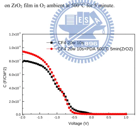
Fig. 4-1 and Fig. 4-2 shows the comparison of C-V curves of the samples with and without PDA treatment on ZrO2 film in O2 ambient at 500°C for 5 minute. In
addition, Fig. 4-2 shows the C-V characteristics of Si surface (before ZrO2 film
deposited) treated CF4 plasma and DC bias 20W for 10 sec.
The characteristics of samples with PDA treatment were improved than samples without treatment. Post deposition annealing could reduce the interface trap density exhibited by more sharp C-V characteristics. The C-V curve of O2-treated PDA 500°C
capacitors was kink free and exhibited good interface properties.
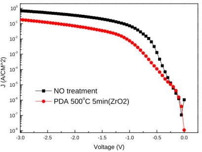
Fig. 4-3 and Fig. 4-4 showed the leakage current density comparison of samples with and without PDA treatment. In addition, Fig. 4-4 shows the J-V characteristics of Si surface (before ZrO2 film deposited) treated CF4 plasma and DC bias 20W for 10 sec.
It can be observed that the samples which treated by PDA treatment present the smaller leakage current density than the leakage current density without PDA treatment. Form leakage density current reveled that a suitable PDA temperature can further improve the dielectric properties.
The hysteresis of C-V characteristics was shown in Fig. 4-5, Fig. 4-6, Fig.4-7, and Fig. 4-8 for the samples with and without PDA treatment. The hysteresis phenomenon of the C-V curves can be observed for all samples, which is caused by the existence of negative charges trapped in the dielectric defect states when the capacitors are stressed. The samples without PDA treatment revealed large hysteresis. Indicate O2-treated PDA
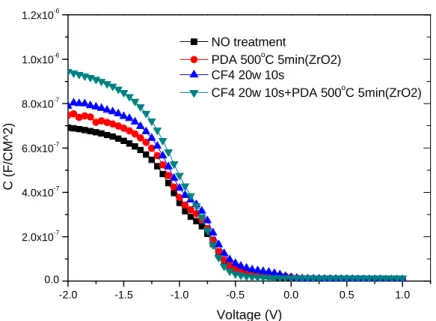
Fig. 4-9 and Fig. 4-10 showed the C-V and the J-V characteristics of samples with various process treatments such as PDA treatment and fluorination treatment. We compared with these treatment and without on electrical characteristics.
In this chapter, we demonstrate that samples treated by PDA treatment and fluorination treatment were the best choice and PDA process can effectively improve gate dielectric quality.
4.2 Electrical characteristics for ZrO
2/HfO
2with nitridation plasma
treatment
The various surface treatments such as without treatment, nitridation, and PDA treatment are compared and studied.
4.2.1Electrical characteristics for ZrO
2/HfO
2with N
2plasma treatment
but without PDA treatment on ZrO
2Fig. 4-11 reveals the capacitance-voltage (C-V) characteristics of samples treated in N2 plasma for 30 sec and 90 sec.The capacitor treated in N2 for 90 sec shows the
maximum capacitance density among these samples with different process treatment.In addition, the capacitors treated for 30 sec also present the larger values than the capacitors without whole plasma nitridation process.
This phenomenon indicates that the N2 plasma treatment was workable to
improve the capacitance. The factor of improvement might be from that the nitrogen incorporation in the HfO2 dielectrics, which could enhance the electronic polarization as
well as the ionic polarization, so the dielectric constant of the HfO2 thin films increases
just as Hf-silicate thin film and SiO2 thin film.
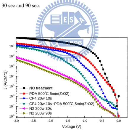
The J-V characteristics of samples treated by N2 plasma with 30 sec and 90 sec
from 0V to -2V are described in Fig. 4-12. It can be observed that the samples which treated in N2 plasma all present the smaller leakage current density than the leakage
![Fig. 2-2 After CF 4 plasma treatment, inner-interface trapping model of HfO 2 for (a) sweeping from accumulation (Vg = -3 V), (b) sweeping from inversion (Vg = 0 V) [39]](https://thumb-ap.123doks.com/thumbv2/9libinfo/8043908.162024/65.892.179.724.213.446/plasma-treatment-interface-trapping-sweeping-accumulation-sweeping-inversion.webp)

![HPSH [ 氧化數平衡反應式係數 ]](data:image/gif;base64,R0lGODlhAQABAIAAAP///wAAACH5BAEAAAAALAAAAAABAAEAAAICRAEAOw==)