Abstract—This paper presents a low voltage on-chip oscillator which can compensate process, voltage, and temperature (PVT) variation in an all-digital manner. The relative reference modeling applies a pair of ring oscillators as relative references and esti-mates period of the internal ring oscillator. The period estimation is parameterized by a second-order polynomial. Accordingly, the oscillator compensates frequency variations in a frequency divi-sion fashion. A 1–20 MHz adjustable oscillator is implemented in a 90-nm CMOS technology with 0.04 mm area. The fabricated chips are robust to variations of supply voltage from 0.9 to 1.1 V and temperature range from 0 C to 75 C. The low supply voltage and the small area make it suitable for low-cost and low-power systems.
Index Terms—Digitally controlled oscillator (DCO), frequency compensation, low voltage, oscillators, process, voltage, and tem-perature (PVT) variations.
I. INTRODUCTION
C
LOCKING is an essential part in a digital system. The conventional clock source, a quartz crystal oscillator, is incompatible with the CMOS process. The incompatibility not only results in extra cost in the board-level integration but also wastes power on the peripheral capacitive elements when passing the oscillation signal. In applications such as microcon-trollers [1] and wireless sensor nodes [2], the cost and power consumption of the overall system are the most concerned for mass distribution and long lifetime. The frequency accuracy can be loosed for the low-cost and low-power integration of the CMOS on-chip oscillators.However, maintaining the frequency accuracy is still a challenging issue of the CMOS on-chip oscillator design due to the process, voltage, and temperature (PVT) variations. Taking a 21-stage ring oscillator in a 90-nm CMOS process as an example, the free-run frequency varies widely from a few hundred MHz to several GHz with PVT variations. Process variation is generally calibrated by trimming passive compo-nents like resistors and capacitors during post-fabrication test. Voltage and temperature variations are dealt with by separate
Manuscript received March 03, 2011; revised May 30, 2011; accepted June 10, 2011. Date of publication August 18, 2011; date of current version July 05, 2012. This work was supported in part by MOEA of Taiwan, under Grant 96-EC-17-A-03-S1-0005, and UMC University Shuttle Program, respectively. The authors are with the Department of Electronics Engineering and Institute of Electronics, National Chiao Tung University, Hsinchu 300, Taiwan (e-mail: [email protected]; [email protected]; [email protected]).
Color versions of one or more of the figures in this paper are available online at http://ieeexplore.ieee.org.
Digital Object Identifier 10.1109/TVLSI.2011.2160301
approaches to maintain the frequency stability. Bandgap ref-erences in [3]–[6] are applied to mitigate voltage variation. Power averaging feedback in [7] cancels the voltage variation. Adaptive biasing scheme [3] is developed for a ring oscillator to maintain a constant frequency over process and temperature variations. A varactor array and feedback loops in [4] compen-sate temperature variation. Proportional to absolute temperature (PTAT) circuits [5] are designed to compensate temperature variation of the reference current and the electron mobility. The resistive elements in [6] and [7] are either chosen or sized for less temperature dependence. These techniques perform excellent capabilities to overcome PVT variations. However, these designs are customized with diagnostic structures and might be dedicated to specific techniques or properties (e.g., bipolar, MIM capacitor, low temperature dependent resistor, etc.). Some are not necessarily available in the fabrication process.
In addition, conventional bandgap references are inappli-cable with sub-1 V supply [8]. The standard supply voltage for the core devices is scaled down to 1 V in deep-submicrometer processes. Circuits operating at low supply voltage have finite voltage headroom for biasing. The existing on-chip oscillators are, therefore, infeasible as the process and the voltage scale shrinks. On the other hand, fully digital implementation can operate at low supply voltage and is easy to be adopted in ex-isting systems. Thus, this work proposes an all-digital solution for a low cost, low voltage on-chip oscillator while maintaining moderate frequency accuracy. The relative reference modeling uses a unified approach to estimate the present oscillation period of a ring oscillator regardless of the individual effects from PVT variations.
The implementation is carried out in a 90-nm CMOS process with the standard supply voltage of 1 V. Two additional con-tributions are further satisfied for various application require-ments: 1) standard logic cell synthesizability, which can be di-rectly combined into existing systems and design flows with negligibly extra effort; 2) frequency adjustability, which can be applied to dynamic frequency scaling applications for power re-duction. The previous work [9] demonstrates a 40 MHz on-chip oscillator where the parallel comparison architecture occupies considerable area. This paper analyzes the frequency accuracy against PVT variations and improves the circuit architecture for area reduction. Section II shows the basic concept of the relative reference modeling. The system architecture and detailed cir-cuits are shown in Section III. Section IV demonstrates the chip implementation and the experimental results. Finally, Section V concludes this work.
Fig. 1. Periods of the ring oscillators composed of different logic gates with voltage and temperature variations. INV: inverter gate, ND:NANDgate; NR:NORgate; the number attached after the gate name indicates the number of inputs.
II. RELATIVEREFERENCE MODELING
The simplest implementation of a fully digital oscillator is the ring architecture composed of odd number of inverting delay cells (IDCs). The basic IDC is an inverter (INV) gate. Some common logic gates, likeNAND,NORgates, can also be config-ured as the IDCs by connecting inputs together. Fig. 1 shows the periods of ring oscillators composed of several types of the IDCs. The cell delays spread widely with voltage and temper-ature variations. Besides, the degrees of the delay variations differ according to the types of the IDCs. Based on the rela-tive delay variations, the relarela-tive reference modeling estimates the absolute value of the gate delay. Denoting the IDC to be modeled as the reference delay cell (RDC) and the IDC to be compared as the compared delay cell (CDC), the delay ratio is expressed as
(1)
where and are the delays of
the CDC and the RDC, respectively. Symbols are expressed as functions of , , and to describe the PVT effects where represents the combined set of plural process parameters. The upper part of Fig. 2 shows the relation between the INV gate delay and the delay ratio of the NR2 gate to the INV gate de-rived from Fig. 1. The INV gate delay is highly correlated to the delay ratio. The delay of the RDC can then be modeled as
(2) where is the th-order modeling coefficient. An approxi-mated second-order polynomial, , is set to model the INV gate delay.
Fig. 2. Upper part shows the simulated points of the INV gate delay to the delay ratio with a second-order model; the lower part shows the modeling error.
In the upper part of Fig. 2, the displacements of the ratio-delay relation caused by voltage and temperature effects are not identical. The two effects span a region that does not coincide on the modeling curve. To evaluate the accuracy of the model, the modeling error is defined as
(3)
The of the is shown in the lower part of
Fig. 2 where the absolute maximum value is 14.2%. The mod-eling accuracy depends on the type of the relative references and the operating range including the supply voltage and the temperature. Two principles should be satisfied for high mod-eling accuracy when selecting the relative reference pairs. First, large relative delay variations exist between the RDC and the CDC so that the absolute delay value can be reflected by the delay ratio. If the delay variations are similar, the delay ratio remains unchanged in different voltage and temperature con-ditions. Second, the displacements of the ratio-delay relation caused by voltage and temperature effects need to be identical. The delay is perfectly modeled if a displacement of the delay ratio, , caused from the voltage or the temperature effect al-ways results in a displacement of the delay, , according to the modeling polynomial.
To get more insights about the selection of the relative refer-ences, the absolute maximum modeling errors of some common logic gates with 0.9 to 1.1 V supply voltage and 0 C to 75 C temperature range are listed in Table I. The model fits better with the relative references of theINV-NANDpairs and theINV-NOR
pairs for the large relative delay variations. TheNAND/NORgates
are more voltage and temperature sensitive than the INVgate
due to the higher equivalent RC delay [10]. When the number of the gate inputs increases, the stacked transistors have higher threshold voltage due to the body effect and become more sen-sitive to the supply voltage. Therefore, the slope of the dis-placement caused by voltage effect gets close to that caused by temperature effect. The absolute maximum modeling errors de-crease as the number of the gate inputs inde-creases. For the rela-tive references of the rest pairs, the above two principles are not
ND:NANDgate; NR:NORgate; the number attached after the gate name
indicates the number of inputs.
Fig. 3. Ratio-delay relation of theINV-NR4 pairs in five process corners. The first letter denotes the speed of the nMOS. The second letter denotes the speed of the pMOS.
well satisfied. The modeling accuracy is inferior and might not be adoptable in applications.
The modeling polynomial can be first-order, second-order, or even higher order depending on the required accuracy. The process variation of the design is implicitly contained in the modeling coefficients, which can be obtained in chip testing pro-cedures. Fig. 3 shows the ratio-delay relations of theINV-NR4
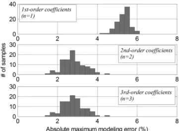
pairs in five process corners. The coefficients alter as the process variations are taken into account, and the Monte Carlo simula-tion1shows the model is still representative. Fig. 4 shows the collections of 100 Monte Carlo simulations with model of dif-ferent polynomial orders. The absolute maximum modeling er-rors are lower when applying higher polynomial orders. How-ever, the improvement of the modeling errors with the polyno-mial order is limited on the order higher than third. It comes to the suggestion that second or third order polynomial is enough for the delay model.
III. SYSTEMARCHITECTURE
A system architecture based on the relative reference modeling is proposed as shown in Fig. 5. The delay ratio esti-mator first estimates the delay ratio of the relative references, . With the estimated delay ratio and the coefficients, the mapper is able to obtain the delay information in the present
1The UMC 90-nm LOGIC/MIXED_MODE Monte Carlo Mismatch Spice
Model is applied with 3 sigma distributions in the process simulations.
Fig. 4. Collections of the absolute maximum modeling errors with different modeling polynomial orders.
Fig. 5. System architecture of the on-chip oscillator.
PVT condition. The control code is then calculated for a digi-tally controlled oscillator (DCO) to generate the compensated clock. One implementation has been carried out in [9] where the parallel-delay-line comparison in the delay ratio estimator occupies considerable area. In this section, we introduce the area-efficient circuit architecture with the period comparisons of two ring oscillators and the frequency compensation based on frequency division.
A. Delay Ratio Estimator
Since the period of a ring oscillator is proportional to the delay of the composite IDCs, the delay ratio of two types of gates can be estimated by the architecture of two ring oscillators shown in Fig. 6. The delay ratio can be estimated with extend-able accuracy requirement by cycle counting. Denoting the ring oscillator with the RDC as RRO and the other with the CDC as CRO, the RRO and the CRO generate oscillation signals which are directly connected to two counters. The estimated delay ratio will be demonstrated as the fractional value
(4) where and are the counted numbers of the CRO and the RRO, respectively. If the counting time is enlarged, the values of and will be bigger and result in a finer estimation resolution. Setting the counting time as cy-cles of the oscillation period of the CRO, the estimation error to the actual period ratio, , is guaranteed to be less than . Setting to the value of power of two,
Fig. 6. Circuit of the delay ratio estimator.
Fig. 7. Circuit of the DCO.
the division by needs no divider. Comparing to the par-allel-delay-line comparison approach [9], the cycle counting ap-proach reduces most of the area which also relieves the effects from the on-die variations.
B. Mapper
Code for the DCO can be calculated in the mapper once the delay ratio is estimated. The second-ordered estimated period of the PRRO is
(5) where is the jth order coefficients. The control code is derived for a desired frequency, , as
(6) It is rounded to the nearest integer due to the finite resolution of the DCO.
C. Digitally Controlled Oscillator
Fig. 7 shows the DCO architecture. The output frequency is an integer fraction of the frequency generated by a pre-output RRO (PRRO). The control code, Code, is compared with the cycle counter. The value of the output register is inverted in every trigger from the comparator output. Therefore, the duty cycle of the output clock is guaranteed to be 50%, and the cor-responding frequency is generated as
(7)
where is the frequency of the PRRO. The
PRRO adopts the same IDCs as the RRO in the delay path and has the same timing performance as estimated to PVT
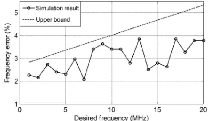
Fig. 8. Simulated output frequency error versus different desired output frequency.
variations. It also eliminates the possible inaccuracy from the path selector of the DCO in [9].
IV. IMPLEMENTATION ANDEXPERIMENTALRESULT
An all-digital on-chip oscillator is implemented in a 90-nm CMOS process based on the above circuit architecture. The INV gate and the NR4 gate are chosen to be the relative references. The supported frequency range with the DCO of 10-bit control code can be as low as 1 MHz. The frequency error versus the desired frequency is shown in Fig. 8. The frequency error is de-fined as the absolute maximum difference between the output frequency and the desired value over the supply voltage from 0.9 to 1.1 V and the temperature range from 0 C to 75 C. The frequency error is presented randomly because of the quantiza-tion effect in the implementaquantiza-tion. A theoretical upper bound for the frequency error can be derived from the absolute maximum modeling error, the worst quantization error, and the worst DCO resolution in the operating range, as
(8) where the implemented quantization error is about 0.1% and
represented for the desired output period.
The frequency error is about two to three percent at lower de-sired frequency. The DCO output frequency resolution might introduce considerable frequency error at higher desired fre-quency. Therefore, the high desired frequency should be con-strained for different application requirements. The simulation result confirms the frequency error is generally larger at higher desired frequency and never exceeds the upper bound. In prac-tice, the upper bound is seldom touched because the probability when the worst modeling error, quantization error, and the DCO resolution happen at the same instant is low.
Fig. 9 shows the die photo with the layout view. It is mounted in the Side Braze ceramic package. The active area is 305 m 130 m including an extra testing part. The area is mainly oc-cupied by the mapper, which handles most of the digital value calculations. The rest parts are regular structures as shown in
Adjustable output frequency.
Fig. 9. Die photo of the on-chip oscillator and the layout view. The floor-plan representations are: (a) delay ratio estimator, (b) mapper, (c) DCO, and (d) testing circuit.
Fig. 10. Measured output frequency of the proposed oscillator when the desired frequency is set as 5 MHz.
the previous section and occupy only a little area. The mod-eling coefficients are first calculated by minimum mean square error fitting from the measurements of the and the in the operating range of the supply voltage from 0.9 to 1.1 V and the temperature from 0 C to 75 C. Fig. 10 shows the mea-sured output frequency for a single sample targeting on 5 MHz. The output frequency is compensated to 5 MHz with 2.3% and 1.6% variations. The start-up time of the output clock is 10.06 s which includes the delay ratio estimation time, the combina-tional circuit delay in the mapper and the DCO delay. The rms jitter and current consumption measured at 5 MHz are 0.24 ns and 650 A, respectively, at 1 V supply and 25 C. A batch test of five chips is executed, and Fig. 11 shows the frequency error versus different output frequency which well corresponds to the simulation results in Fig. 8.
Comparing to the previous work [9], this work reduces the area by more than 10 times. The implementation of the pe-riod comparison can also improve the frequency accuracy with a longer calibration time due to the cycle counting. The fre-quency division based compensation occupies smaller area, and
Fig. 11. Measured output frequency error of 5 samples at different output frequency.
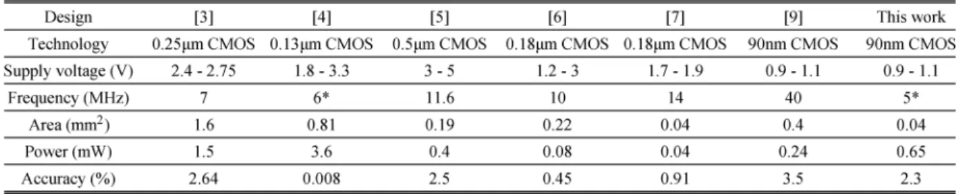
the output matches the delay model without extra error in the delay path. As to the existing on-chip oscillators, the perfor-mance comparison is listed in Table II. In this work, the archi-tecture with the relative reference modeling is the first all-dig-ital approach to compensate the output frequency to PVT vari-ations. The advantages of the lowest supply voltage and the smallest area are achieved with moderate frequency accuracy. The proposed on-chip oscillator can be directly integrated in the deep-submicrometer design with the standard supply voltage of 1 V. In addition, the utilization of the standard logic and the fre-quency adjustability make it more applicable to various system requirements.
V. CONCLUSION
A relative reference modeling method has been proposed to estimate the period of the internal ring oscillator affected by PVT variations. The architecture of the period comparison based delay ratio estimation and the frequency division based compensation is implemented in a 90-nm CMOS process. Targeting on 5 MHz, the measurement shows the maximum frequency error of 2.3%. The proposed on-chip oscillator works at lower supply voltage in standard CMOS process and can be fully integrated in existing systems for low-cost and low-power applications.
ACKNOWLEDGMENT
The authors would like to thank their colleagues within the SI2 Group, National Chiao Tung University, Taiwan, for many fruitful discussions in test chip design and implementation.
REFERENCES
[1] E. D. Marsman, R. M. Senger, M. S. McCorquodale, M. R. Guthaus, R. A. Ravindran, G. S. Dasika, S. A. Mahlke, and R. B. Brown, “A 16-bit low-power microcontroller with monolithic MEMS-LC clocking,” in
Proc. IEEE Int. Symp. Circuits Syst., 2005, pp. 624–627.
[2] M. Patel and J. Wang, “Applications, challenges, and prospective in emerging body area networking technologies,” IEEE Wirel. Commun., vol. 17, no. 1, pp. 80–88, Feb. 2010.
[3] K. Sundaresan, P. E. Allen, and F. Ayazi, “Process and temperature compensation in a 7-MHz CMOS clock oscillator,” IEEE J. Solid-State
Circuits, vol. 41, no. 2, pp. 433–442, Feb. 2006.
[4] M. S. McCorquodale, B. Gupta, W. E. Armstrong, R. Beaudouin, G. Carichner, P. Chaudhari, N. Fayyaz, N. Gaskin, J. Kuhn, D. Linebarger, E. Marsman, J. O’Day, S. Pernia, and D. Senderowicz, “A silicon die as a frequency source,” in Proc. IEEE Int. Freq. Control Symp., 2010, pp. 103–108.
[5] A. V. Boas and A. Olmos, “A temperature compensated digitally trimmable on-chip IC oscillator with low voltage inhibit capability,” in Proc. IEEE Int. Symp. Circuits Syst., 2004, pp. 501–504.
[6] J. Lee and S. Cho, “A 10 MHz 80 W 67 ppm C CMOS refer-ence clock oscillator with a temperature compensated feedback loop in 0.18 m CMOS,” in Symp. VLSI Circuits Dig. Tech. Papers, 2009, pp. 226–227.
[7] Y. Tokunaga, S. Sakiyama, A. Matsumoto, and S. Dosho, “An on-chip CMOS relaxation oscillator with power averaging feedback using a ref-erence proportional to supply voltage,” in IEEE Int. Solid-State Circuit
Conf. Dig. Tech. Papers, 2009, pp. 404–405.
[8] M. D. Ker and J. S. Chen, “New curvature-compensation technique for CMOS bandgap reference with sub-1-V operation,” IEEE Trans.
Circuits Syst. II, Exp. Briefs, vol. 53, no. 8, pp. 667–671, Aug. 2006.
[9] C. Y. Yu, J. Y. Yu, and C. Y. Lee, “An eCrystal oscillator with self-calibration capability,” in Proc. IEEE Int. Symp. Circuits Syst., 2009, pp. 237–240.
[10] T. Sakurai and A. R. Newton, “Delay analysis of series-connected MOSFET circuits,” IEEE J. Solid-State Circuits, vol. 26, no. 2, pp. 122–131, Feb. 1991.
Chien-Ying Yu was born in Hsinchu City, Taiwan, in 1984. He received the B.S. degree in electronics engineering from National Chiao-Tung University, Hsinchu, Taiwan, in 2006, where he is currently pursuing the Ph.D. degree in electronics engineering. His research interests include VLSI architec-ture, low-power SoC, and wireless communication systems, especially in OFDM-based baseband trans-ceiver for low-power WBAN systems and on-chip oscillator design.
Jui-Yuan Yu was born in Taipei City, Taiwan, in 1979. He received the B.S. and Ph.D. degrees in electronics engineering from National Chiao-Tung University, Hsinchu, Taiwan, in 2002 and 2008, respectively.
He is currently serving as a Postdoctoral Re-searcher with National Chiao-Tung University. His research interests include VLSI architecture, low-power SoC, and wireless communication systems, especially in OFDM-based baseband transceiver for high-speed WLAN, ultra-wideband (UWB) systems, and low-power WBAN systems.
Chen-Yi Lee (M’01) received the B.S. degree from National Chiao Tung University, Hsinchu, Taiwan, in 1982, and the M.S. and Ph.D. degrees from Katholieke University Leuven (KUL), Leuven, Belgium, in 1986 and 1990, respectively, all in electrical engineering.
From 1986 to 1990, he was with IMEC/VSDM, working in the area of architecture synthesis for DSP. In February 1991, he joined the faculty of the Electronics Engineering Department, National Chiao Tung University, Hsinchu, Taiwan, where he is currently a Professor and Dean of the Research and Development Office. His research interests mainly include VLSI algorithms and architectures for high-throughput DSP applications. He is also active in various aspects of high-speed networking, system-on-chip design technology, very low power designs, and multimedia signal processing. In these areas, he has authored or coauthored more than 180 papers and holds decades of patents.
Dr. Lee served as the Director of Chip Implementation Center (CIC), an or-ganization for IC design promotion in Taiwan (2000/2008–2003/2012), and the microelectronics program coordinator of the Engineering Division under the National Science Council of Taiwan (2003/2001–2005/2012). Dr. Lee was the former IEEE Circuits and Systems Society Taipei Chapter Chair.