www.nature.com/scientificreports
A Novel Read Scheme for Large
Size One-Resistor Resistive
Random Access Memory Array
Mohammed Zackriya V
1,2, Harish M. Kittur
2& Albert Chin
1The major issue of RRAM is the uneven sneak path that limits the array size. For the first time record large One-Resistor (1R) RRAM array of 128x128 is realized, and the array cells at the worst case still have good Low-/High-Resistive State (LRS/HRS) current difference of 378 nA/16 nA, even without using the selector device. This array has extremely low read current of 9.7 μA due to both low-current RRAM device and circuit interaction, where a novel and simple scheme of a reference point by half selected cell and a differential amplifier (DA) were implemented in the circuit design.
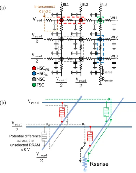
The RRAM implemented in crosspoint array structure promises high scalability and 3D architecture. A RRAM cell is placed in each intersecting point of Word-Line (WL) and Bit-Line (BL) as shown in Fig. 1(a). During write phase, the RRAM cell is programmed to HRS (Roff) or LRS (Ron) to store 0 or 1. To read the resistive state of a
RRAM cell, a potential difference of a read voltage (Vread) is applied to the cell and is termed as Full Selected Cell
(FSC). The remaining Non-Selected Cells (NSCs) in the array are biased at 0 potential difference between their terminals. Among various biasing schemes for NSCs, the Vread/2 method has lower voltage swing and low power
consumption. As shown in Fig. 1(a), to read the state of selected cell at 1 × 3, WL1 is pulled to Vread while the BL3
is grounded. Rest of the WLs and BLs are biased atVread/2. The current passing through the Rsense determines the
state of the selected RRAM cell. Here the NSCs with one terminal connected to either WL1 or BL3, has potential difference of Vread/2 between their terminals. These cells are defined as Half Selected Cells (HSC). These HSCs
create sneak path to influence the current passing through Rsense. As shown in a simple 2 × 2 RRAM array of
Fig. 1(b), although a RRAM cell at 1 × 2 (green color) is selected; other paths (grey color) through the HSCs can direct current to Rsense and disturb the actual current flowing through the selected cell. Thus effective resistance
(Reff) which is calculated w.r.t. current flowing through the selected BL and Vread applied at the WL gets disturbed.
The sneak current is much more severe as the array size increases and it is data pattern dependent. The worst case for usual crosspoint array is when the read cell is at HRS while all other cells are at LRS or vice versa1–6.
To address the sneak path issue, the RRAM devices (1 R) were proposed in series with a diode (1D1R), a transistor (1T1R) and a selector (1S1R)1–4. Other works have been presented which aim on architectural design
(device + circuit interaction) to effectively detect the state of RRAM cell in the presence of sneak current5,6. In this
paper, we present a novel architecture: record large 1 R RRAM array of 128 × 128 is realized with ultra-low read current of 9.7 μ A by this scheme, even without selector device. This is possible because the sneak path current is used as reference input for the DA, and the current change of a selected cell from HSC to FSC is much higher at LRS than HRS to differentiate the stored 1 or 0 state.
Methods
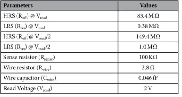
To reach the low set/reset power, we pioneered the covalent-bond-dielectric GeOx RRAM device7,8. Very low
HRS/LRS currents were achieved by carrier hopping conduction rather than the high current via shorted metallic filament. To further control the process-induced resistance variation, similar covalent-bonded SiOx RRAM device
was used in this study. Figure 2 shows the I-V hysteresis curves of Ni/SiOx/TaN RRAM device. This RRAM cell
offers large HRS/LRS ratio that is crucial to reach a large size memory array. Besides, the low LRS current allows low power read operation. Table 1 comprises of RRAM device parameters. External reference circuit becomes impractical because of device to device resistance variation. To consider this issue, we have taken lowest HRS and highest LRS to realize the read scheme. Here Vread was chosen carefully, as high Vread will increase the sneak
current. The HRS of the device biased at Vread and Vread/2 are 83.4 and 149.4 MΩ respectively. Similarly the LRS 1Department of Electronics Engineering, National Chiao Tung University, Hsinchu 300, Taiwan. 2School of Electronics
Engineering, VIT University, Vellore, India. Correspondence and requests for materials should be addressed to A.C. (email: [email protected])
received: 05 October 2016 Accepted: 13 January 2017 Published: 10 February 2017
of the device biased at Vread and Vread/2 are 0.38 and 1.0 MΩ respectively. Such high resistance values are crucial
to save the read power in a large RRAM array. These parameters were used for simulation to realize an effective read scheme. The proposed architecture determines the state of RRAM cell in an array by considering the current through HSCs and current slope of the FSC. Thus the worst case for the proposed architecture is, when the FSC Figure 1. (a) 2D structure of RRAM crosspoint array. Rsense– Sense Resistor; FSC– Full Selected Cell; NSC– Non Selected Cell; HSCWL/BL– Half Selected Cell WL/BL, (b) 3D structure of 2 × 2 RRAM crosspoint array.
Green, red & grey cells are FSC, HSC and NSC resp. Actual and leakage current– green & grey path resp.
Figure 2. I-V hysteresis curves of Ni/SiOX/TaN RRAM. The large HRS/LRS ratio is the merit for this device
www.nature.com/scientificreports/
(last bit of first word) is of HRS (or LRS) and remaining bits are also at HRS (or LRS). The worst case data pattern for the FSC to be HRS and LRS are defined as WCH and WCL, respectively. The impact of sneak path increases
with the array size and has more impact on WCLthan WCH. This is because WCL has all the cells at LRS in HSC
state (LRSHSC); thus, these LRSHSCs leak more current through sneak path via resistive network to the selected BL.
Results
Background Analysis for Proposed Design.
While reading a particular RRAM cell in the crosspoint array, its corresponding WL and BL are assigned to Vread and ground respectively. Initially, both WL and BL wereat Vread/2 potential. As shown in Fig. 3(a), when a cell in BL2 of a 2 × 2 RRAM array is to be read, the BL2 goes to
ground. All the cells in BL2 are HSCs (red) and rest of the cells in other BLs are NSCs (grey). The current flowing
Parameters Values
HRS (Roff) @ Vread 83.4 M Ω
LRS (Ron) @ Vread 0.38 MΩ
HRS (Roff)@ Vread/2 149.4 MΩ
LRS (Ron) @ Vread/2 1.0 MΩ
Sense resistor (Rsense) 100 KΩ
Wire resistor (Rwire) 2.8 Ω
Wire capacitor (Cwire) 0.046 fF
Read Voltage (Vread) 2 V
Table 1. Device parameters used for read operation.
Figure 3. (a) 3D structure of 2 × 2 RRAM crosspoint array – cell to be read is located in BL2 and thus it is grounded to measure the leakage current in BL2, and (b) Partial 3D structure of 2 × 2 RRAM crosspoint array – Green cell is to be read. (a) BL2 is grounded; (b) BL and WL are selected (WL1 to Vread and BL2 to 0 V).
through Rsense is purely the contribution made by the HSCs of the BL2. When the WL1 is assigned to Vread from
Vread/2, only the selected cell (green) on BL2 goes from HSC to FSC as shown in Fig. 3(b). When the selected cell
moves from HSC to FSC state, the cell resistance reduces and the current through the cell increases. Yet, extra leakage current flows from WL2 to BL2 (dark grey), as it carries leakage current from HSCWL as well as HSCBL.
As shown in Fig. 4(a), the current difference on I-V curves of RRAM between Vread/2 and Vread is much higher
for LRS than HRS. Thus, when the selected cell changes from HSC to FSC, the change in current is very high if the selected cell is LRS compared to HRS. It is further shown in Fig. 4(b,c), the plot of current difference when the WL1 is selected and moving from Vread/2 to Vread for WCH and WCL respectively. Even as the array size increases,
WCH remains less than WCL. For the best case, the current difference is further less and more while reading HRS
(< WCH) and LRS (> WCL) cell respectively. It can be noticed that, as the array size increases, the difference in
current is falling down. This is because of sneak current offered by WL. The DA design9 can detect Δ V
in as low as
10 mV with an offset of about 5~8 mV. Thus, with Rsense of 100 KΩ , the DA can detect the state of 1 R RRAM cell
in an array as large as 128 × 128 (voltage difference at input of DA for WCL is 43.5 mV). Beyond 128 × 128 array
size, the detectable voltage difference goes below 10 mV. Here the read current for this sized array is only 9.7 μ A. The 128 × 128 array size is the largest among 1 R RRAM arrays and proposed architecture is the only architecture Figure 4. (a) Generic switching behavior of RRAM – swept I-V curves. HRS and LRS curves are in green and red colors resp., (b) Difference in current on selected bitline when the corresponding selected wordline is at Vread and Vread/2 for worst-case data pattern, WCH, and (c) Difference in current on selected bitline when the
www.nature.com/scientificreports/
available which is close to 1S1R RRAM arrays. This is the basic concept leading to use the reference point by HSC and a DA for circuit design.
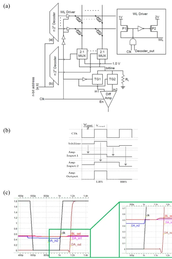
Architectural Implementation.
A RRAM crosspoint array architecture synchronized with a clock is pre-sented in Fig. 5(a). Input address drives the row and column decoder to select the WL driver and MUX. Once a MUX is selected, the corresponding BL is grounded through Rsense. While the WL driver, Transmission Gate (TG)and DA are controlled by the clock. The inset of Fig. 5(a) shows the WL driver circuit, selected WL is held at 2 V (Vread) when clock is at level-1 and at 1 V (Vread/2) rest of the time. When the clock is low (to read the cell at 1 × 2),
Figure 5. (a) Proposed architecture for novel read scheme - a nxn RRAM crosspoint array with differential amplifier. TG – Transmission Gate | MUX – Multiplexer, (b) Ideal timing waveform of the proposed read scheme, and (c) The simulated waveform of the proposed read scheme for worst case data pattern, WCL.
WL driver holds the WL1 at Vread/2 and through TG1, in1 of DA is charged to the potential of BL2. Similarly,
when clock is high, WL driver drives WL1 to Vread and through TG2, in2 of DA is charged to the potential of
BL2 (while TG1 isolates in1 from BL2, thus in1 replicates the charge on BL2 when WL1 was Vread/2). The DA is
enabled to positive level of the clock to determine the state of selected cell. The operation is further explained in Fig. 5(b); when the clock is low, sneak current through the HSCs (biased at Vread/2) in BL is captured at the input1
(reference) of DA. As the clock goes high, the potential difference across selected cell becomes Vread and the
corresponding current is captured on the other input of the DA to determine the resistive state. Buffer is placed between clock and driver, so that clock has sufficient time to turn on and off the TG2 and TG1 respectively, before the driver sets a bias voltage of Vread on SC. Simulation result is shown in Fig. 5(c); the DA output goes high as
the clock becomes high to indicate the SC is at LRS. The enlarged version of waveform is presented in the inset of Fig. 5(c), in1 of DA follows BL (SC is biased at Vread/2) when the clock is low. As soon as the clock goes high,
SC is still biased at Vread/2 to avoid disturbance on in1 and thus in1, in2 and BL remains at same potential. After
a delay of buffer, the driver sets bias of Vread on SC, at this moment in2 of DA follows BL and the DA detects the
state of SC. The simulation was performed in HSPICE using TSMC 0.18 μ m technology, while modeling and pro-gramming was with MATLAB. As presented in Table 2, the design has considered both capacitor and resistor of interconnects during simulation. With the proposed read scheme and low switching power RRAM cell, the stored state of RRAM cell in a 128 × 128 array can be effectively determined even without the selector. This is the largest size among any array presented in literature for 1 R RRAM1–3,6, even close to among those with 1S1R devices1–3.
Besides, the 1S1R device has low resistance in the range of KΩ at LRS, which consumes ~3 orders of magnitude more power than this 1 R device in MΩ range. These devices also consume very low power compared to DRAM; yet the speed is 2~3 orders of magnitude slower.
Conclusion
A novel read scheme is proposed that effectively reads a 1 R cell in an array of 128 × 128. The scheme determines the state of RRAM cell from the difference of the current when the selected WL is at Vread/2 and Vread. This scheme
predicts the leakage current through the HSCs in BL and further extending to predict leakage through both BL and WL.
References
1. Zhou, J., Kim, K. H. & Lu, W. Crossbar RRAM arrays: Selector device requirements during read operation. IEEE Trans. Electron Devices. 61, 1369–1376 (2014).
2. Deng, Y. et al. RRAM crossbar array with cell selection device: A device and circuit interaction study. IEEE Trans. Electron Devices.
60, 719–726 (2013).
3. Jo, S. H., Kumar, T., Narayanan, S., Lu, W. D. & Nazarian, H. 3D-stackable crossbar resistive memory based on field assisted superlinear threshold (FAST) selector. IEDM Tech. Dig. 160–163 (2014).
4. Zhang, L. et al. On the optimal on/off resistance ratio for resistive switching element in one-selector one-resistor crosspoint arrays. IEEE Electron Device Lett. 36, 570–572 (2015).
5. Chen, B. et al. Efficient in-memory computing architecture based on crossbar arrays. IEDM Tech. Dig. 459–462 (2015).
6. Liu, C. & Li, H. A weighted sensing scheme for ReRAM-based cross-point memory array. IEEE Computer Soc. Annual Symp. on VLSI Tech. Dig. 65–70 (2014).
7. Cheng, C. H., Chin, A. & Yeh, F. S. Novel ultra-low power RRAM with good endurance and retention. Symp. on VLSI Tech. Dig. 85–86 (2010).
8. Cheng, C. H., Tsai, C. Y., Chin, A. & Yeh, F. S. High performance ultra-low energy RRAM with good retention and endurance. IEDM Tech. Dig. 448–451 (2010).
9. Schinkel, D., Mensink, E., Klumperink, E., Tuijl, E. V. & Nauta, B. A double-tail latch-type voltage sense amplifier with 18ps setup + hold time. ISSCC Tech. Dig. 314–605 (2007).
Acknowledgements
This paper’s publication was supported in part by Ministry of Science and Technology of Taiwan.
Author Contributions
Mohammed Zackriya V contributed to the RRAM architecture, circuit simulation, and wrote the manuscript; Albert Chin contributed to the RRAM device, RRAM architecture, circuit simulation and wrote the manuscript with Mohammed Zackriya V together and provided the financial support for this work; Harish M Kittur is the co-supervisor for Mohammed Zackriya V and studied the RRAM architecture. All authors reviewed the manuscript.
Additional Information
Supplementary information accompanies this paper at http://www.nature.com/srep Competing financial interests: The authors declare no competing financial interests.
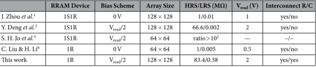
RRAM Device Bias Scheme Array Size HRS/LRS (MΩ) Vread (V) Interconnect R/C
J. Zhou et al.1 1S1R 0 V 128 × 128 1/0.01 1 yes/no
Y. Deng et al.2 1S1R V
read/2 128 × 128 66.6/0.002 2 yes/no
S. H. Jo et al.3 1S1R V
read/2 64 × 64 ratio> 102 — –/–
C. Liu & H. Li6 1R 0 V 64 × 64 1/0.005 0.5 yes/no
This work 1R Vread/2 128 × 128 83.4/0.38 2 yes/yes
www.nature.com/scientificreports/
How to cite this article: Zackriya, M. et al. A Novel Read Scheme for Large Size One-Resistor Resistive Random Access Memory Array. Sci. Rep. 7, 42375; doi: 10.1038/srep42375 (2017).
Publisher's note: Springer Nature remains neutral with regard to jurisdictional claims in published maps and institutional affiliations.
This work is licensed under a Creative Commons Attribution 4.0 International License. The images or other third party material in this article are included in the article’s Creative Commons license, unless indicated otherwise in the credit line; if the material is not included under the Creative Commons license, users will need to obtain permission from the license holder to reproduce the material. To view a copy of this license, visit http://creativecommons.org/licenses/by/4.0/