Using FPGA to Implement a Partial Reconfigurable Architecture of Embedded System
4
0
0
全文
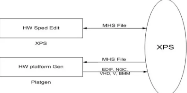
(2) Int. Computer Symposium, Dec. 15-17, 2004, Taipei, Taiwan.. Microprocessor unit MicroBlaze (32-bits soft CPU) Application logic unit EMC (External memory controller)、GPIO (General-purpose I/O) 、UART Memory unit LMB BRAM (On-Chip memory) Communication interface unit OPB (On-chip Peripheral Bus) 、LMB (Local memory bus) Standard peripheral RS232、7-segment LED、LED、DIP Switch、 Push Button. 2.3. Development Environment In software, we use several EDA (Electronic Design Automation) tools to help us complete our design. Xininx© ISE (Integrated Software Environment) can run synthesis 、 implementation then produce bit-stream file to download to chip. Modeltech© ModelSim can execute functional simulation and EDK (Embedded Development Kit) support many tools to develop embedded system. In hardware, we use development board of Memec©, DS-KIT-V2MB1000-EURO, it provides a FPGA chip with 1,000,000 gate count and others resource.. 3. Design and Implementation 3.1. Establish Hardware Structure The design flow of hardware platform is showed in Figure 3 and defined by the MHS (Microprocessor Hardware Specification) file [4][5]. The hardware platform consists of one or more processors and peripherals connected to the processor buses. Users can define their own peripherals and combine them in the MHS. The MHS file is a simple text file.. Figure 1. System Structure. 2.2. Reconfigurable Computing Architecture A reconfigurable computing architecture combines one major MPU and many reconfigurable function units. The MPU control system operation and reconfigurable hardware deal with data operation. The reconfigurable function unit can be treated as co-processor to accelerate specific operation. Reconfigurable computing architecture is showed in Figure 2. It includes a programmable MPU on left-hand side and a reconfigurable function unit on right-hand side. We can replace core1 by core2 via JBit copy [1][2]. According to the demand for specific function, system can dynamic change [3] the architecture of hardware to satisfy different kinds of application.. Figure 3. Design Flow of Hardware Platform The MHS file defines the system structure 、 peripherals and embedded processors. It also defines the connectivity of the system, the address map of each peripheral in the system and configurable options for each peripheral. The PlatGen (Platform Generator) tool creates the hardware platform using the MHS file as input. PlatGen produces net-list files of various forms, for example, NGC or EDIF file. Those files can be used by downstream tool to download to FPGA chip. Top-level HDL wrappers allow user to generate modular IP [6][7] that can be partial reconfigurable. Figure 4 shows how to generate modular IP.. 3.2. Establish Software Environment and Application Program Figure 2. Reconfigurable Computing Architecture. The software platform is defined by the MSS (Microprocessor Software Specification) file. The. 2 951.
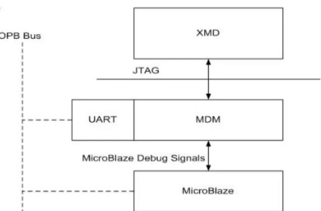
(3) Int. Computer Symposium, Dec. 15-17, 2004, Taipei, Taiwan.. MSS file defines customization parameters of driver and library for peripherals、processor customization parameters 、 standard input and output devices 、 interrupt handler routines and other related software features. The MSS file is also a simple text file and used as input by the LibGen (Library Generator) tool for customization of drivers 、 libraries and interrupts handlers.. Figure 6. Integral Verification Flow 3.3.1. Functional Simulation. The verification platform is based on the hardware platform. The verification specification allows the user to specify a simulation model for each processor, peripheral or other module in the hardware platform. The MHS file is processed by the SimGen (Simulation Generator) tool to create simulation files along with some command files for specific simulators supported by the tool. 3.3.2. Applications Debug. XMD (Xilinx Microprocessor Debugger) and the GDB (GNU debugger) are used together to debug the application software. XMD provides an instruction set simulator, and optionally connects to a working hardware platform to allow GDB to run the user application. When the device is configured, we can debug the software application directly via the MDM (MicroBlaze Debug Module) interface. GDB connects to the MicroBlaze core through the MDM and the XMD engine utility as shown in Figure 7. XMD is a program that facilitates a unified GDB interface and a Tcl (Tool Command Language) interface for debugging programs and verifying systems using the MicroBlaze microprocessor.. Figure 4. Generate Modular IP The source code of the application program can be written in a high level language such as C or C++ or in assembly language. Once the source files was created, GNU compiler compile the source file and link to generate executable files in the ELF (Executable and Link Format) format. Entire process of creating the software platform and application program is shown in Figure 5.. Figure 5. Design Flow of S/W Platform and Application. 3.3. Integral Verification. Figure 7. Run Application and Debug. In this step, we can separate two independent directions: functional simulation and application debug. The verification flow of design can be shown in Figure 6.. 3 952.
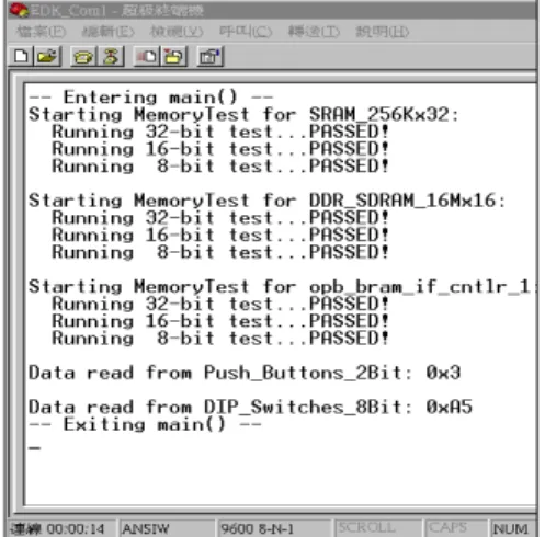
(4) Int. Computer Symposium, Dec. 15-17, 2004, Taipei, Taiwan.. 4. Verification Summarize our design with following results: As we follow the design flow to complete our design, we must verify and test the design whether it work normally. We can look over the PBD (Processor Block Diagram) file to check all connection of hardware module whether it is correct or not. We will also load our application program into on-chip memory of FPGA and execute the application program. Utilize serial cable to connect PC and development board and then the result finally will be shown on the terminal window of PC. Figure 8 shows our system test diagram.. Total Number LUTs: 2,503 out of 10,240 24% Number of Block RAMs: 16 out of 40 40% Number of MULT18X18s: 3 out of 40 7% Total equivalent gate count for design: 1,155,751 Maximum frequency: 76.982MHz. 5. Conclusion Our paper proposes a design flow for partial reconfigurable architecture of embedded system. We can design many application logic units beforehand, then download specific bit-stream file to FPGA chip according to specific requirement. The new application logic unit can aid main microprocessor to handle large amount and special operation. This design of partial reconfigurable architecture includes flexibility and efficiency both. We plan to extend our work into the following directions: 1. Construct a prototype with fully selfreconfiguration system. 2. Develop multi-function of embedded system employing multiple reconfigurable coprocessors connected via on-chip busses.. Serial Cable. Figure 8. System Testing Diagram We run a test program to write one data of 32-bits (AAAA5555H)、16-bits (AA55H) and 8-bits (A5H) to SRAM、DDR_SDRAM and OPB_RAM module. When these data have read from the above memory, we will check if the data corresponds to wrote value previously then show the “PASSED!” message on the terminal windows, otherwise show “FAILED!”. At the same time, we test the input/output device on the development board. The test program receives data from the input device (DIP_Switch and Push _Button) and show the value on the terminal. We can also write data to the output device (7_segment LED and 1-bit LED), it will form horse race light on the two 7_segment LED. The test result will be shown in Figure 9.. References [1] E. L. Horta and J. W. Lockwood. “PARBIT: A Tool to Transform Bitfiles to Implement Partial Reconfiguration of Field Programmable Gate Arrays (FPGA).” Technical report, Department of Computer Science, Applied Research Lab, Washington University, Saint Louis, July 2001. [2] Matthias Dyer, Christian Plessl, and Marco Platzner. “Partially Reconfigurable Cores for Xilinx Virtex”, Computer Engineering and Networks Lab, ETH Zurich, 2002. [3] Chien-Kuei Chung. “Design and Implement of Dynamic Reconfigurable Architecture Base on Embedded System”, July 23, 2004. [4] Xilinx, Inc. “Embedded System Tools Reference Guide”, January 30, 2004. [5] Xilinx, Inc. “Platform Studio User Guide”, January 30, 2003. [6] Xilinx, Inc. “OPB IPIF Product Specification”, June 14, 2004. [7] Xilinx, Inc. “User Core Templates Reference Guide”, January, 2004.. Figure 9. Test Result. 4 953.
(5)
數據
相關文件
In this paper, by using the special structure of circular cone, we mainly establish the B-subdifferential (the approach we considered here is more directly and depended on the
• Supports program binaries compiled for a different instruction set than the. host hardware
Microphone and 600 ohm line conduits shall be mechanically and electrically connected to receptacle boxes and electrically grounded to the audio system ground point.. Lines in
This bioinformatic machine is a PC cluster structure using special hardware to accelerate dynamic programming, genetic algorithm and data mining algorithm.. In this machine,
Filter coefficients of the biorthogonal 9/7-5/3 wavelet low-pass filter are quantized before implementation in the high-speed computation hardware In the proposed architectures,
In this thesis, we develop a multiple-level fault injection tool and verification flow in SystemC design platform.. The user can set the parameters of the fault injection
Community of practice provides a platform for knowledge workers to share, learn and discuss the knowledge related to a particular topic, thus, the performance of the community
The main purpose of this paper is using Java language with object-oriented and cross platform characteristics and Macromedia Dreamweaver MX to establish a JSP web site with
