The Enhancement of Nitrogen Incorporation in RTN
2O
Annealed TEOS Oxide Fabricated on Disilane-Based
Polysilicon Films
Jam Wem Lee, Won-Der Chen, Tan Fu Lei, and Chung-Len Lee Department of Electronics Engineering, National Chiao Tung University, Hsinchu, Taiwan
Disilane-based stacked structures were first proposed to demonstrate that the nitrogen incorporation was enhanced in the RTN2O annealed tetraethylorthosilicate共TEOS兲 oxide fabricated on disilane-based polysilicon films. Compared with the oxide fabricated on the silane-based polysilicon film, the nitrogen incorporation in the disilane-based oxides is six times higher. To study the nitrogen incorporation effects on the RTN2O annealed TEOS oxides, the disilane-based polysilicon stacked on the silane-based polysilicon film structure was proposed. We found that the oxide quality was largely improved by the same surface morphology of bottom polysilicon films. We think the this approach could be used in fabricating dynamic random access memory共DRAM兲 to have better data retention characteristics and to improve the reliability of DRAM and flash memory devices.
© 2001 The Electrochemical Society. 关DOI: 10.1149/1.1383554兴 All rights reserved.
Manuscript submitted January 7, 2001; revised manuscript received April 17, 2001. Available electronically July 13, 2001.
Polyoxide with a low leakage current and a high stress endurance capability is essential in obtaining good data retention characteristics of the novel dynamic random access memory 共DRAM兲 and flash memory devices. However, polyoxide has a higher leakage current and a relatively lower breakdown field than oxides grown on single crystalline silicon.1-4
Recently, the ONO 共oxide/nitride/oxide兲 stacked films were widely used as an interpoly dielectric in fabricating DRAM and flash memory devices because of its low leakage current and good electrical endurance capability. Unfortunately, the stacked structure suffers a scaling down problem.5To obtain a highly reliable thin polysilicon insulator, the tetraethylorthosilicate共TEOS兲 oxides be-ing nitrided in N2O ambient by rapid thermal process were proposed.6The quality of the nitrided TEOS oxides, however, was found to be highly dependent on the surface morphology of the polysilicon films on which they were deposited. According to this correlation, the polysilicon films with a smooth surface were fabri-cated to produce highly reliable polyoxides. Discouragingly, reduc-ing the surface roughness of the polysilicon will reduce the capaci-tance of the capacitor, therefore limiting its application to fabricating DRAM devices. The nitrogen incorporation also strongly affected the quality of the oxides; that is, increasing the nitrogen incorpora-tion increased the reliability of the nitrided TEOS polyoxides. Therefore, in order to improve the quality of TEOS oxide without changing the surface morphology of polysilicon, a higher nitrogen incorporation is needed.
The nitrided oxides fabricated on the disilane-based polysilicon films were proposed in our previous work.7In that work, we found that the fabricated polyoxides had better reliability than the conven-tional ones. The improvement could be due to the smoother surface of the bottom disilane-based polysilicon films and the higher nitro-gen incorporation of the prepared oxides; however, the effects of those factors were mixed together.
In this paper, the disilane stacked polysilicon film structures are proposed to demonstrate higher nitrogen incorporation. As a result, the proposed oxide was found to have better reliability without changing the surface morphology of bottom polysilicon films, mainly with the much higher nitrogen incorporation.
Experimental
At first, two conventional polysilicon films 2000 Å thick were prepared by two different deposition conditions. The polysilicon with a rough surface was deposited using silane gas at 620°C in low pressure ambient and the smooth polysilicon was deposited by using disilane gas at 470°C. Then the polysilicon films were implanted with a phosphorus dose of 5⫻ 1015at energy of 30 keV and an-nealed at 950°C in a rapid thermal N2ambient for 30 s. The sheet resistance for conventional polysilicon films deposited by silane and
disilane were 130 and 70⍀/䊐, respectively. In addition, the surface roughness 共rms兲 measured from atomic force microscope 共AFM兲 indicated that it is 30 Å for silane deposited film and 3 Å for disilane deposited film.
The stacked polysilicon films were fabricated by depositing a 300 Å nondoped polysilicon film on the previous prepared conven-tional polysilicon films by using disilane gas at 470°C in a low pressure furnace ambient. The sheet resistance and the surface roughness of the stacked films were the same with the conventional films共i.e., 130 ⍀/䊐 and 30 Å of disilane stacked on silane polysili-con film, 70⍀/䊐 and 3 Å of disilane stacked on disilane polysilicon film, respectively.兲
The two conventional polysilicon films and two kinds of stacked polysilicon films were prepared as the polyIs of the capacitors. After the polyIs was prepared, they were RCA cleaned and deposited on a 100 Å TEOS oxide. After the oxide deposition was completed, all samples were annealed at 950°C in a rapid thermal N2O ambient (RTN2O兲 and the final thickness of the oxides was 130 Å.
All samples were then deposited with a 3000 Å polysilicon film to be used as the gate material共polyII兲 by using silane gas at 620°C in a low pressure ambient. Then, the polysilicon films were POCl3 doped at 850°C in a N2ambient for 1 h to achieve a sheet resistance of 40⍀/䊐. The polyIIs were then patterned and grown with a 1000 Å passivation oxide. After contact holes of polyIs and polyIIs were opened, Al film was deposited, patterned, and sintered at 350°C for 40 min in an N2ambient to be used as the electrodes of the capaci-tors.
The sheet resistance was measured by using the four-point probe method, the surface rms was measured by atomic force microscopy 共AFM兲 and thickness was determined by capacitance voltage 共CV兲 measurement. Finally, we used HP 4145b to measure the J-E, Ebd,Qbd, and the electron trapping characteristics.
Results and Discussion
Figure 1 shows the AFM images of the polyI surfaces of the nonstacked polysilicon films and the stacked ones. They are共a兲 S the polysilicon deposited by using silane,共b兲 D the polysilicon de-posited by using disilane, 共c兲 SD the silane-based polysilicon stacked with disilane-based polysilicon,共d兲 DD the disilane-based polysilicon stacked with disilane-based polysilicon, 共e兲 SS the silane-based polysilicon stacked with silane-based polysilicon, and 共f兲 DS the disilane-based polysilicon stacked with silane-based poly-silicon. We can easily find that the surface roughness共rms兲 of the nonstacked films, graphs共a兲 and 共b兲, and the disilane-stacked films, graphs 共c兲 and 共d兲 are nearly the same, respectively. This implies that the top disilane film does not affect the surface roughness of the polysilicon films. On the other hand, the surface roughness of the DS sample is rougher than the DD and the D samples. The increase Journal of The Electrochemical Society, 148共8兲 F164-F169 共2001兲
0013-4651/2001/148共8兲/F164/6/$7.00 © The Electrochemical Society, Inc. F164
of the roughness resulted from the higher nucleation rate occurring during the polysilicon deposition at higher temperature. It can be seen that the surface roughness of disilane polysilicon increases from 3 to 13 Å after adding a 300 Å silane-based polysilicon as shown in共f兲. Nevertheless, to maintain the integrity of polyoxide, the stacked films 共e兲 and 共f兲 deposited by using silane were not performed in this research.
Figure 2 shows the nitrogen共N兲 and phosphorus 共P兲 SIMS pro-files of the stacked and the nonstacked samples. The P concentration in the top disilane-based films was slightly higher than that in the lower conventional polysilicon films. This means that the top disi-lane films could be unintentionally doped during the following ther-mal process. The N profiles are also presented in this figure. The N concentration in the disilane共D兲, the disilane/disilane 共DD兲, and the silane/disilane共SD兲 samples is much higher than that of the silane 共S兲 sample. The result indicates that the N atoms are easier to incor-porate into the dibased polysilicon film than into the silane-based polysilicon film. This should be due to the fact that relatively
lower activation energy is enough to form bonding between silicon and nitrogen impurities for the disilane-based polysilicon. The varia-tion activavaria-tion energy for the silane-based and disilane-based films could be caused by the microstructural difference of these two films, which has been studied in Ref. 8. The microstructural difference of disilane-based and silane-based films is shown in Fig. 3; this figure presents that the dominant structures are具110典 and 具111典 for silane sample while具111典 for disilane.
The disilane stacked on disilane 共DD兲 sample has a slightly higher N concentration than the disilane stacked on silane 共SD兲 sample in the polyoxide, which could be ascribed to the smooth surface of the disilane samples. Therefore, the N profile of the DD sample is much sharper than that of the SD sample.
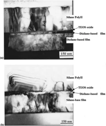
Figure 4 shows the TEM of the共a兲 DD and 共b兲 SD samples. We can find that the disilane-based polysilicon film is conformal stacked on the conventional polysilicon films. This explains why the non-stacked films have similar surface roughness to the disilane non-stacked films. Additionally, the interface between the top disilane stacked Figure 1. AFM images of the共a兲 S 共silane兲, 共b兲 D 共disilane兲, 共c兲 SD 共silane stacked with disilane兲, 共d兲 DD 共disilane stacked with disilane兲, 共e兲 SS 共silane stacked
with silane兲 and 共f兲 DS 共disilane stacked with silane兲. The rms of the surface roughness is 3, 0.3, 3, 0.3, 3, and 1.3 nm, respectively.
film and bottom conventional films could be observed clearly. With this interface, the impurities that reduce oxide reliability could be trapped; therefore, improve the reliability of the oxides.
Figure 5 shows the J-E characteristics of the共a兲 D and DD, 共b兲 S and SD samples with both polarities. We found that the stacked structure could improve the leakage characteristics of the oxides; especially for S and SD samples.
Figure 6 shows the effective barrier heights of the oxides, which were extracted from the J-E characteristics by using the method mentioned in Ref. 10. The figure indicates that the oxides deposited on the stacked structure polysilicon films have higher barrier height than those deposited on the nonstacked polysilicon films do. This is especially true when the polyIIs are positively biased. The improve-ment can be attributed to the fact that, while the oxides annealed in rapid thermal N2O ambient, the bottom conventional polysilicon films being isolated by the top disilane stacked polysilicon film. Therefore, a 30 Å higher quality N2O grown thermal oxide could be achieved by preventing it from contacting with the defects, which remained in bottom conventional polysilicon films during doping process 共i.e., implantation and rapid thermal annealing兲. Note that the difference between the S and SD samples is much larger than the difference between D and DD samples. The result could be because there is much higher nitrogen incorporation in the SD sample than
that in the S sample while similar nitrogen distribution of the D and DD samples is shown in Fig. 2.
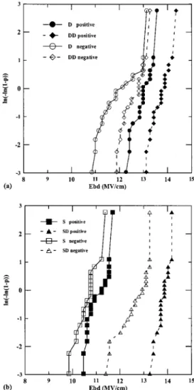
Figure 7 shows the Weibull plots of the electric field to break-down (Ebd) of the共a兲 D and DD, 共b兲 S and SD with both polarities. We found that the disilane-stacked films have better Ebd character-istic than the nonstacked ones, especially for the SD and S samples. Figure 8 shows the trapping charge characteristics of the共a兲 DD and D and 共b兲 SD and S samples 共the stress current density is 1 mA/cm2兲. We found that the stacked samples have a lower electron-trapping rate, and therefore, higher Qbddistributions. The figure also presents that the DD, SD, and D samples have hole trapping while polyII is positively stressed. This indicates that those samples have higher N incorporation within the oxides because similar phenom-enon were observed for the reported nitrogen-rich oxides prepared by N2O or NO.9,10
Figure 9 presents the Weibull plots of the charge to breakdown (Qbd) 共the stress current density is 10 mA/cm2兲 of the stacked and the nonstacked samples, they are共a兲 D and DD, 共b兲 S and SD with both polarities. The stacked samples have a higher Qbddistribution, that is, the disilane-based stacked films can improve the quality of polyoxides. Roughly speaking, the disilane-based stacked oxides are improved about two orders of magnitude in Qbd than that of the nonstacked silane polyoxide and about one order of magnitude than that of the nonstacked disilane polyoxide. The improvement can be attributed to the fact that, while depositing or annealing TEOS ox-Figure 2. SIMS profiles of the共a兲 phosphorus, 共P兲 count, and 共b兲 nitrogen
共N兲 count of the disilane 共D兲, disilane stacked with disilane 共DD兲, silane
stacked with disilane共SD兲, and silane 共S兲, respectively.
Figure 3. XRD patterns of the共a兲 disilane and 共b兲 silane samples.
Journal of The Electrochemical Society, 148共8兲 F164-F169 共2001兲 F166
ides, the bottom polysilicon films being isolated by the top disilane polysilicon film. Therefore, the polyoxide layers can prevent them-selves from contacting with the defects, which remain in the lower conventional polysilicon during doping process. Moreover, the higher N concentration incorporated into polyoxide can be another factor in improving the quality of the silane polyoxide, which can be observed with the SIMS profiles in the Fig. 2.
Conclusions
The TEOS oxides deposited on disilane-based polysilicon films were shown to have higher nitrogen incorporation. The enhancement could be due to the microstructure difference between the disilane-based and silane-disilane-based polysilicon films. The higher nitrogen incor-poration could improve the characteristics of the oxides; therefore, with the disilane-based polysilicon film stacked structure, the poly-oxides could have better quality without changing the surface rough-ness of the polysilicon.
The effects on the defects and impurities produced during im-plantation process were also found to be eliminated by adding this thin film.
Acknowledgment
This work was supported by NSC 89-2215-E-009-095, NSC 89-2218-E-009-069, and the SRC of National Chiao-Tung University.
The authors assisted in meeting the publication costs of this article. Figure 4. TEM images of the共a兲 DD 共disilane stacked with disilane兲 and 共b兲
SD共silane stacked with disilane兲 samples.
Figure 5. J-E characteristics of the共a兲 D and DD, 共b兲 S, and SD samples with both polarities.
Figure 6. The effective barrier height of the four prepared oxide samples with both polarities.
Figure 7. The Weibull plots of Ebdof the共a兲 D 共disilane兲 and DD 共disilane
stacked with disilane兲 samples with both polarities, 共b兲 S 共silane兲 and SD
共silane stacked with disilane兲 samples with both polarities.
Figure 8. Charge trapping characteristics of the prepared samples.共a兲 DD and D,共b兲 SD and S samples with both polarities. The stressed current is 1 mA/cm2. The injection charge is calculated from the formula
q⫽J (A/cm2)t(s). The gate voltage shift is calculated from the formula
delta V(t)⫽ V(t) ⫺ V(t ⫽ 0).
Figure 9. The Weibull plots of Qbdof the共a兲 D 共disilane兲 and DD 共disilane stacked with disilane兲 samples with both polarities, 共b兲 S 共silane兲 and SD 共silane
stacked with disilane兲 samples with both polarities.
Journal of The Electrochemical Society, 148共8兲 F164-F169 共2001兲 F168
References
1. C. H. Kao, C. S. Lai, and C. L. Lee, IEEE Electron Device Lett., 44, 526共1997兲. 2. L. Faraone, IEEE Trans. Electron Devices, 33, 1785共1986兲.
3. S. L. Wu, T. Y. Lin, C. L. Lee, and T. F. Lei, IEEE Electron Devices Lett., 14, 113 共1994兲.
4. S. L. Wu, C. Y. Chen, T. Y. Lin, C. L. Lee, T. F. Lei, and M. S. Liang, IEEE Trans. Electron Devices, 44, 153共1997兲.
5. C. H. Kao, C. S. Lai, and C. L. Lee, IEEE Trans. Electron Devices, 45, 1927 共1998兲.
6. J. W. Lee, C. L. Lee, T. F. Lei, and C. S. Lai, IEEE Trans. Electron Devices,共2001兲. 7. E. G. Lee and J. J. Kim, Thin Solid Films, 226, 123共1993兲.
8. H. Hwang, W. Ting, D. L. Kwong, and J. Lee, Tech. Dig. Int. Electron Devices Mat., 1990.
9. M. Bhat, J. Kim, J. Yan, G. W. Yoon, L. K. Han, and D. L. Kwong, IEEE Electron Device Lett., 15, 421共1994兲.
10. L. Faraone, R. D. Vibronek, and J. T. Mcginn, IEEE Trans. Electron Devices, 32, 577共1985兲.