Growth of carbon nanotube field emitters in the triode structure
using anodic aluminum oxide as the template
Chen-Chun Lin
a, Kai-Chun Chang
a, Fu-Ming Pan
a,⁎
, Cheng-Tzu Kuo
a,
Mai Liu
b, Chi-Neng Mo
baDepartment of Materials Science and Engineering, National Chiao-Tung University, Hsinchu, Taiwan bChunghwa Picture Tubes, Ltd., Taoyuan, Taiwan
Available online 8 February 2007
Abstract
Carbon nanotubes (CNT) were grown in anodic aluminum oxide (AAO) and used as field emitters in a triode structure. To fabricate the field-emission triode structure, nanoporous anodic aluminum oxide (AAO) thin layer was first prepared on the Si(100) substrate, followed by the growth of vertically aligned carbon nanotubes in AAO pore channels by electron cyclotron resonance chemical vapor deposition (ECR-CVD). The SiO2dielectric and Al gate electrode layers required for the triode structure were directly deposited on the CNTs. Reactive ion and wet etches were then used to open the field-emission area in the triode. Scanning electron microscopy and Raman spectroscopy studies revealed that damage to CNT emitters in the etched area was trivial. Field-emission characteristics of the CNT emitters have been studied and an anode turn-on electric field of∼8.05 V/μm was measured.
© 2007 Elsevier B.V. All rights reserved.
Keywords: Carbon nanotubes (CNT); Anodic aluminum oxide (AAO); Field-emission
1. Introduction
Carbon nanotubes (CNT) have many desirable properties as a source of field electron emitters, such as high aspect ratio, small radius of curvature, high mechanical strength and chemical stability [1–3]. Therefore, carbon nanotubes have attracted wide interest in the development of field-emission flat panel displays (FED) using CNTs as field emitters. For FED applications, it is necessary to grow vertically aligned CNT arrays on a large area with suitable tube density and tube diameters[4–6]. In many CNT-FED studies, CNT emitters on the cathode panel are prepared either by direct catalytic chemical vapor deposition or screen printing [7–11]. Field screen effect often degrades field-emission properties of CNT emitters grown by CVD method because the density of CNTs is usually too high to avoid field penetration among adjacent emitters[12]. On the other hand, the screen printing method has difficulties to make uniform and well-aligned CNT emitters on the substrate. In our previous study, we have successfully grown
vertically aligned and uniform CNTs in the porous anodic aluminum oxide (AAO) template, which was prepared on the Si (100) substrate, by electron cyclotron resonance chemical vapor deposition (ECR-CVD)[13,14]. Both the density and length of CNT emitters can be well controlled by tuning the CVD deposition conditions, such as the composition of the gas precursor and growth time. In this study, we fabricated field-emission triode arrays with the AAO templated carbon nanotubes as the field emitters by standard integrated circuit processes. The field-emission property of the CNT emitters in the triode structure was also studied.
2. Experimental
An Al film 2μm thick was first evaporation-deposited on the p-type Si(100) wafer, and the AAO pore channel array was subsequently prepared by electrochemical anodization in oxalic acid solution. In order to obtain well-aligned pore channels, the AAO fabrication was carried out with the two-step anodization method. Anodization was first carried out in a 0.3 M oxalic acid solution at 21 °C under a constant polarization voltage of 40 V for 5 min. The thus formed nanoporous AAO about 1μm thick
⁎ Corresponding author. Tel.: +886 3 5731322; fax: +886 3 5724727. E-mail address:[email protected](F.-M. Pan).
0925-9635/$ - see front matter © 2007 Elsevier B.V. All rights reserved. doi:10.1016/j.diamond.2007.01.034
was removed by wet chemical etching at 60 °C with a mixture solution of H3PO4 and CrO3, thereby leaving a relatively
ordered indent pattern on the surface of the Al film. The second anodization of the indented Al film was then performed for 4 min under the same anodization condition as the first one. After the second anodization step, the AAO barrier layer removal and pore widening were performed by etching the as-prepared AAO film in a 5 wt.% H3PO4solution at 30 °C for
40 min. This resulted in highly uniform and periodic nanoporous channels in the AAO layer, which were then used as the template for the growth of carbon nanotubes. A metallic Al layer∼300 nm thick was left on the wafer surface after the AAO fabrication, and was used as the bottom electrode. Cobalt was used as the catalyst for CNT growth, and was electro-chemically deposited at the AAO pore bottom in the mixture electrolyte of CoSO4and H3BO3. The CNT growth was carried
out at 600 °C in an ECR-CVD system using a gas mixture of 20% CH4and 80% H2as the plasma source for 30 min. During
the CNT growth, the ECR-CVD system was under the following operation conditions: magnetic field strength 875 G, microwave power 750 W, substrate bias −100 V, working pressure ∼2×10− 3 Torr and deposition temperature
600 °C. The carbon nanotubes grown in the AAO template as described above will be abbreviated as AAO-CNT thereafter in the text.
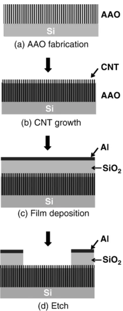
To fabricate AAO-CNT field-emission triodes, standard integrated circuit processes were used. Fig. 1 shows the fabrication scheme of the triode array. After the preparation of the AAO-CNT emitters, tetraethoxysilane (TEOS) oxide was deposited on the AAO-CNT layer as the dielectric layer of the triode by plasma enhanced CVD (PE-CVD), and followed by the evaporation–deposition of an Al layer as the gate electrode. The pattern of triodes with a diameter of 6.5 μm was photolithographically defined by a mask aligner (Karl-Suss MJB-3). The Al top layer was etched by a high density plasma reactive ion etch (HDP-RIE) system using the gas mixture of BCl3and Cl2as the etchant source. The oxide dielectric was
then RIE etched using a gas mixture of CHF3and Ar as the
plasma source. After the RIE process, buffered oxide etchant (BOE) was used to remove the remnant SiO2.
Scanning electron microscopy (JEOL JSM-6700) was used to characterize the morphology of the AAO-CNTs and the triodes. The chemical and microstructure properties of AAO-CNTs were studied by Raman spectroscopy (He–Ne laser, Jobin Yvon LABBRAM). Field-emission measurement was per-formed with a Keithley 2410 electrical measurement system. 3. Results and discussion
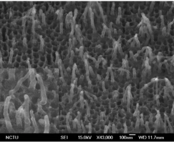
The nanoporous AAO film exhibited highly ordered pore arrangement with a uniform pore size of 70 nm–80 nm and a pore-to-pore separation about 100 nm. This allows the Co catalyst to be uniformly deposited at the bottom of each vertical pore channel by electro-deposition and acted as catalysts to grow CNTs. Using AAO as the template, the CNTs grew along the axis of pore channels and had a tube diameter compliant with the pore size of the AAO pore channels, resulting in the growth of uniform diameter and well-aligned CNTs. In our previous studies, the length and tube density of CNTs extending out of the AAO pore channels could be properly controlled by the growth time and the gas ratio of CH4and H2in the
ECR-CVD system, respectively [13,14]. Fig. 2(a) shows the side-view micrograph of the nanoporous AAO template. After the CNT growth for 30 min, the length extending out of the AAO pore surface of most CNTs was ∼400 nm. The tube number density of CNT was as high as 3 × 10⁹ tubes/cm2, which corresponded to one third of the pore density of the AAO template. Although, the CNTs seemed to be randomly distributed on the AAO template, but the tube number density was controllable and reproducible. During the CNT growth in the CH4/H2 plasma, amorphous carbon byproduct was also
deposited on the AAO surface. Some carbon nanotubes were found to be blocked in the nanopores by the amorphous carbon residual and unable to grow out of the pore surface. Co catalyst particles were found to locate at the tip of the carbon nanotubes, indicating that CNT growth in AAO nanopore channels was via the tip growth mode.
To fabricate AAO-CNT field-emission triodes, the dielectric layer and the gate electrode layer were directly deposited on the
Fig. 1. The fabrication scheme of the AAO-CNT triode structure: (a) preparation of the AAO layer on the Si wafer, (b) CNT growth by ECR-CVD deposition, (c) dielectric and gate electrode depositions on the CNTs, and (d) RIE and BOE etches to open the field-emission area of the triode.
CNT emitters grown on the AAO template. All CNTs were embedded in the SiO2dielectric layer of 1.5μm in thickness as
shown in the cross-sectional SEM micrograph ofFig. 2(b). The surface roughness of the SiO2 dielectric layer was strongly
influenced by the length of CNTs extending out of AAO channels and the thickness of the SiO2layer. Therefore an appropriate
combination of the length of CNTs and the thickness of the dielectric layer is crucial to photolithographically define the pattern of the field-emission triode array. After photolitho-graphy, the Al gate layer was reactive ion-etched. The silicon dioxide dielectric layer was then partially removed by RIE using a 50/50% mixture of CHF3and Ar (with a gas flow of 80 sccm) as
the gas source at a pressure of 10 mTorr. After the RIE process, the remnant SiO2was completely removed by BOE wet etching
for 5 s. The gate electrode thus patterned was electrically isolated from the AAO-CNT cathode layer according to resistance measurement using an ohmmeter.Fig. 3shows the SEM image of the AAO-CNT triode array fabricated as described. The triode structure is 6.5μm in diameter and 2 μm in depth.
It is generally believed that ion sputtering can alter the microstructure of carbon nanotubes and thus alter the field-emission property. Carbon nanotubes would suffer from ion bombardment as the CNTs in the triode structure were exposed to the plasma during etching of the SiO2 dielectric. During the
reactive ion etching of the SiO2dielectric layer, a mixture of CHF3
and Ar was used, and thus carbon nanotubes were subject to bombardment of various ions, including hydrogen, fluorine, argon and fluorocarbon ions. It has been reported that hydrogen ion bombardment could increase C–H bondings in carbon nanotubes and resulted in a more disordered microstructure
[15]. On the other hand, fluorination occurs on the carbon nanotubes when CNTs are treated by fluorocarbon plasma, such as CF4[16,17]. In this study, we found that the RIE process to
remove partial SiO2dielectric layer seemed not to cause obvious
damage.Fig. 4shows the SEM image of the AAO-CNT emitters after the dielectric layer was removed by RIE etching for 270 s, followed by BOE etching for 5 s. It can be clearly seen that Co catalyst particles were still present at the tips of the carbon nanotubes, implying that the RIE etching induced little damage to the AAO-CNTs. Difference in the length and density of carbon nanotubes between the as-prepared AAO-CNTs and that after the removal of the dielectric layer was hardly perceivable.Fig. 5
shows the Raman spectra of the as-grown carbon nanotubes on the AAO template and that after the removal of SiO2by RIE and
BOE etches. The two prominent Raman peaks are located at ∼1325 cm− 1(D band) and∼1598 cm− 1(G band). The former is
due to the ring stretching mode in a disordered graphitic structure and the latter to sp2bond stretching mode[18,19]. Peak features of both Raman modes, such as peak position and intensity, are commonly used to study the insight of the crystallinity and
Fig. 3. (a) The SEM image of the AAO-CNT triode array. (b) An enlarged SEM image of a single triode.
Fig. 2. (a) SEM image of the carbon nanotubes grown on the AAO template. (b) Cross-sectional SEM image of the AAO-CNTs capped by the TEOS SiO2
graphitic bonding of carbon nanotubes. The ratio of the integral intensities of the G and D bands, IG/ID, can be used to estimate the
microstructure disorder of carbon nanotubes. The SiO2
encapsu-lated sample had an IG/IDratio about 0.46 after the RIE and BOE
etches, and this value was close to that of the as-prepared AAO-CNTs,∼0.5. In addition, the two Raman peaks of the etched sample had no apparent peak shift as compared to the counterparts of the as-prepared AAO-CNTs, suggesting that the removal of the SiO2 dielectric layer by RIE and BOE etches did not cause
significant chemical and microstructure damage to the carbon nanotubes.
Field-emission measurement of the AAO-CNT triode array was conducted under a vacuum condition of∼10− 6Torr with a simple diode measurement configuration. A cylindrical probe was placed 100μm above the AAO-CNT emitters without any electrical connection to the Al gate electrode. The measured field-emission current density (J ) as a function of the electric field (E) was plotted inFig. 6. The anode turn-on electric field (Eto), which is defined as the electric field required to produce
an emission current density of 1 mA/cm2, was ∼8.05 V/μm. The measured Etowas slightly higher than that of AAO-CNT
emitters with a similar tube density grown on a blanket AAO template previously reported[20]. The emission current density of the CNT emitters in the triode at an anode–cathode voltage of
8.1 V/μm was about one fourth of that of the blanket sample. Because the triode emitter array occupied only one third of the area of the AAO template, it is expected that the measured field-emission density should be smaller for the triode emitters. The Fowler–Nordheim (F–N) plot shown in the inset of Fig. 6
exhibited two linear segments. The two-segment feature of the F–N plot for AAO-CNTs prepared with a high CH4/H2 flow
rate ratio has been reported in our previous work[20]. It was ascribed that amorphous carbon residual deposited on the carbon nanotubes might cause the nonlinear F–N plot. We are setting up a field-emission measurement system, which allows us to apply bias voltage on the Al gate electrode, so that field-emission characteristics of the individual AAO-CNT triodes can be studied.
4. Summary
We have successfully fabricated field-emission triodes with carbon nanotubes as field-emitters. The nanoporous AAO film was used to template the growth of vertically aligned CNT emitters in an ECR-CVD system. Standard IC process techniques were used to fabricate the triode structure on the as-prepared AAO-CNT layer. Reactive ion and BOE etches, which were carried out to etch away the Al gate electrode and the SiO2 dielectric layer in the triode structure, made little
damage to the AAO-CNT emitters according to SEM and Raman spectroscopy studies. An anode turn-on electric field of 8.05 V/μm was obtained for the AAO-CNT emitters in the triode array.
Acknowledgements
This work was supported by the National Science Council of Taiwan, under Contract No. NSC93-2120-M-009-007. Techni-cal support from the National Nano Device Laboratories (NDL) is gratefully acknowledged.
Fig. 6. Field-emission current density (J)–electric field (E) characterization of the AAO-CNT triode array. The inset shows the corresponding Fowler– Nordheim plots.
Fig. 5. Raman spectra of (a) the as-prepared AAO-CNT emitters and (b) the SiO2
capped AAO-CNTs after RIE etching for 270 s and BOE etching for 5 s. Fig. 4. SEM image of the AAO-CNTs after RIE etching for 270 s and BOE etching for 5 s. The inset is an enlarged image of the carbon nanotubes.
References
[1] Andreas Thess, Roland Lee, Pavel Nikolaev, Hongjie Dai, Pierre Petit, Jerome Robert, Chunhui Xu, Young Hee Lee, Seong Gon Kim, Andrew G. Rinzler, Daniel T. Colbert, Gustavo E. Scuseria, David Tománek, John E. Fischer, Richard E. Smalley, Science 273 (1996) 483.
[2] P.G. Collins, A. Zettl, H. Bando, Philip G. Collins, A. Zettl, Hiroshi Bando, Andreas Thess, R.E. Smalley, Science 278 (1997) 100.
[3] Jie Liu, Andrew G. Rinzler, Hongjie Dai, Jason H. Hafner, R. Kelley Bradley, Peter J. Boul, Adrian Lu, Terry Iverson, Konstantin Shelimov, Chad B. Huffman, Fernando Rodriguez-Macias, Young-Seok Shon, T. Randall Lee, Daniel T. Colbert, Richard E. Smalley, Science 280 (1998) 1253.
[4] Y.M. Wong, W.P. Kang, J.L. Davidson, B.K. Choi, W. Hofmeister, J.H. Huang, Diamond Relat. Mater. 15 (2006) 334.
[5] In-Mook Choi, Sam-Yong Woo, Seung-Soo Hong, J. Vac. Sci. Technol., A, Vac. Surf. Films 24 (2006) 1556.
[6] Do Yoon Kim, Ji-Beom Yoo, In Taek Han, Ha Jin Kim, Ha Jong Kim, Jae Eun Jung, Yong Wan Jin, Jong Min Kim, Kyoung-Hwan Chin, Diamond Relat. Mater. 14 (2005) 2084.
[7] Yun-Hi Lee, Yoon-Taek Jang, Dong-Ho Kim, Jin-Ho Ahn, Byeong-kwon Ju, Adv. Mater. 13 (2001) 479.
[8] J.E. Jung, Y.W. Jin, J.H. Choi, Y.J. Park, T.Y. Ko, D.S. Chung, J.W. Kim, J.E. Jang, S.N. Cha, W.K. Yi, S.H. Cho, M.J. Yoon, C.G. Lee, J.H. You, N.S. Lee, J.B. Yoo, J.M. Kim, Physica B 323 (2002) 71.
[9] M.A. Guillorn, M.D. Hale, V.I. Merkulov, M.L. Simpson, G.Y. Eres, H. Cui, A.A. Puretzky, D.B. Geohegan, J. Vac. Sci. Technol., B. 21 (2003) 957.
[10] K.B. Kim, Y.H. Song, C.S. Hwang, C.H. Chung, J.H., I.S. Choi, J.H. Park, J. Vac. Sci. Technol., B. 22 (2004) 1331.
[11] H.J. Lee, Y.D. Lee, W.S. Cho, B.K. Ju, Yun-Hi Lee, J.H. Han, J.K. Kim, Appl. Phys. Lett. 88 (2006) 093115.
[12] L. Nilsson, O. Groening, C. Emmenegger, O. Kuettel, E. Schaller, L. Schlapbach, Appl. Phys. Lett. 76 (2000) 2071.
[13] Po-Lin Chen, Jun-Kai Chang, Fu-Ming Pan, Cheng-Tzu Kuo, Diamond Relat. Mater. 13 (2004) 1949.
[14] Po-Lin Chen, Jun-Kai Chang, Fu-Ming Pan, Cheng-Tzu Kuo, Diamond Relat. Mater. 14 (2005) 804.
[15] C.Y. Zhi, X.D. Bai, E.G. Wang, Appl. Phys. Lett. 81 (2002) 1690. [16] N.O.V. Plank, L. Jiang, R. Cheung, Appl. Phys. Lett. 83 (2003) 2426. [17] A. Felten, C. Bittencourt, J.J. Pireaux, G. Van Lier, J.C. Charlier, J. Appl.
Phys. 98 (2005) 074308.
[18] M.A. Tamor, W.C. Vassell, J. Appl. Phys. 76 (1994) 3823. [19] A.C. Ferrari, J. Robertson, Phys. Rev., B 61 (2000) 14095.
[20] Po-Lin Chen, Jun-Kai Chang, Cheng-Tzu Kuo, Fu-Ming Pan, Appl. Phys. Lett. 86 (2005) 123111.