366 IEEE ELECTRON DEVICE LETTERS, VOL. 28, NO. 5, MAY 2007
Effect of Top Electrode Material on Resistive
Switching Properties of ZrO
2
Film Memory Devices
Chih-Yang Lin, Chen-Yu Wu, Chung-Yi Wu, Tzyh-Cheang Lee, Fu-Liang Yang,
Chenming Hu, Fellow, IEEE, and Tseung-Yuen Tseng, Fellow, IEEE
Abstract—The influence of top electrode material on the
resis-tive switching properties of ZrO2-based memory film using Pt as a bottom electrode was investigated in this letter. In comparison with Pt/ZrO2/Pt and Al/ZrO2/Pt devices, the Ti/ZrO2/Pt device ex-hibits different resistive switching current–voltage(I–V ) curve, which can be traced and reproduced by a dc voltage more than 1000 times only showing a little decrease of resistance ratio be-tween high and low resistance states. Furthermore, the broad dis-persions of resistive switching characteristics in the Pt/ZrO2/Pt and Al/ZrO2/Pt devices are generally observed during successive resistive switching, but those dispersions are suppressed by the device using Ti as a top electrode. The reliability results, such as cycling endurance and continuous readout test, are also presented. The write-read-erase-read operations can be over 104cycles with-out degradation. No data loss is found upon successive readwith-out after performing various endurance cycles.
Index Terms—Nonvolatile memory, resistive random access
memory (RRAM), resistive switching, ZrO2.
I. INTRODUCTION
T
HE next-generation nonvolatile memory (NVM) has at-tracted extensive attention due to the conventional memo-ries approaching their scaling limits. Several types of NVMs, such as ferroelectric random access memory, magnetic ran-dom access memory, and resistive ranran-dom access memory (RRAM), are being investigated. Among various NVMs, the RRAM that is composed of a simple metal-insulator-metal (M-I-M) structure has the merits of low power consumption, high-speed operation, and high-density integration. Due to these excellent characteristics, a number of metal oxides, such as SrZrO3 [1], Pr1−xCaxMnO3 [2], [3], Nb2O5[4], TiO2[5], [6], NiO [7], and ZrO2[8], have been studied. However, there is an important issue risen about how to minimize the dispersions of resistive switching parameters such as the resistance values of ON-state (RON) and OFF-state (ROFF), and the required voltages to switch fromOFF-state toON-state(VON), and vice versa(VOFF), which is needed to overcome. It is because thatManuscript received January 23, 2007. This work was supported in part by the Taiwan Semiconductor Manufacturing Company, Ltd., and in part by the National Science Council, Taiwan, under project NSC 95-2221-E-009-278. The review of this letter was arranged by Editor P. Weiss.
C.-Y. Lin, C.-Y. Wu, C.-Y. Wu, and T.-Y. Tseng are with the Department of Electronics Engineering and Institute of Electronics, National Chiao Tung University, Hsinchu 300, Taiwan R.O.C. (e-mail: [email protected]).
T.-C. Lee and F.-L. Yang are with the Taiwan Semiconductor Manufacturing Company, Ltd., Hsinchu 300, Taiwan R.O.C.
C. Hu is with the Department of Electrical Engineering and Computer Sciences, University of California at Berkeley, Berkeley, CA 94720 USA.
Digital Object Identifier 10.1109/LED.2007.894652
after a long-time operation, the dispersions of these parame-ters lead to severe control and readout hazards. By means of inserting thin IrO2 layers at M–I interfaces, the reduction of dispersion was shown due to the enhancement of crystalline insulator [9]. Moreover, reducing the active memory area to sub-100-nm size by a plug-contact-type bottom electrode was also able to reduce the dispersion into a sharp distribution [10]. In this letter, we report a more effective and convenient method to reduce the dispersions of the resistive switching parameters by replacing conventional Pt or Al top electrode with Ti top electrode.
II. EXPERIMENTS
The 70-nm-thick ZrO2 films were deposited on Pt/Ti/SiO2/Si substrate at 250 ◦C by a radio-frequency (RF) magnetron sputtering. All films were prepared at 10 mtorr, which was maintained by a gas mixture of oxygen and argon at a mixing ratio of 6:12. To achieve the M-I-M structure, the Al top electrode was deposited by a thermal evaporation to fabricate Al/ZrO2/Pt structure. The top electrodes of Pt and Ti were deposited by an RF magnetron sputtering to form Pt/ZrO2/Pt and Ti/ZrO2/Pt structures. All the top electrodes were formed at ambient temperature with a diameter of 250µm patterned by the shadow mask process. Agilent 4155C semi-conductor parameter analyzer was used to measure the current– voltage(I–V ) characteristics of the ZrO2film memory device. For dynamic measurement, Agilent 81110A was employed to generate voltage pulses to change the resistance of the device, and the Agilent 4155C was used to measure the current of the device. All the measurements were performed at room temperature.
III. RESULTS ANDDISCUSSION
Fig. 1(a) shows the typical I–V curve of the Ti/ZrO2/Pt device. First, using the dc voltage sweep method with a current compliance of 5 mA, there, a sudden increase of current occurs near 8.8 V and, then, is limited at 5 mA, which is called forming process. The forming process is similar for all the three devices. After the forming process, the Ti/ZrO2/Pt device reaches its low resistance state, called ON-state. By sweeping a voltage bias to negative over VOFF, the device is switched from the low resistance state to the high resistance state (OFF-state). On the contrary, the voltage sweep toward positive overVON
is performed to switch back to the ON-state, and there is no current compliance needed again, which is different from the
LIN et al.: EFFECT OF TOP ELECTRODE MATERIAL ON SWITCHING PROPERTIES OF ZrO2 367
Fig. 1. Typical resistive switchingI–V curves of Ti/ZrO2/Pt, Pt ZrO2/Pt, and Al ZrO2/Pt devices, respectively.
reported Pt/ZrO2/Pt and Al/ZrO2/Pt devices [11]. The typical
I–V curves of Pt/ZrO2/Pt and Al/ZrO2/Pt devices are unipolar
[as shown in Fig. 1(b)], which apply the positive (negative) voltage to switch them toOFF-state and back toON-state with a current compliance by applying the positive (negative) voltage again. It was reported that the oxygen content and oxygen-related defects had great influences on the resistive switching characteristics [6], [7], [9], [11], [12]. Therefore, the different
I–V curve of Ti/ZrO2/Pt device from those of Pt/ZrO2/Pt
and Al/ZrO2/Pt devices might be attributed to the lower work function (4.3 eV) of titanium, or that titanium served as oxygen gettering material to induce the oxygen vacancies at Ti/ZrO2 interface, which would modify the oxygen vacancies distribu-tion within ZrO2memory film further leading to better resistive switching characteristics.
The resistive switching of Ti/ZrO2/Pt device (I–V curve) can be traced and reproduced over 1000 times. The 10th, 100th, and 1000th cycleI–V curves of Ti/ZrO2/Pt device are shown in Fig. 2, and there is only a little distortion between them. During the successive resistive switching by dc volt-age, there is no “set fail” phenomenon observed, which is a failure of resistive switching from OFF-state to ON-state [9]. Moreover, as the continuous resistive switching cycle increases, the ON-state current (measured at 0.3 V) gradually decreases
Fig. 2. 10th, 100th, and 1000thI–V curves in the Ti/ZrO2/Pt device during continuous dc voltage switching cycles. The inset shows that the current of theON-state gradually decreases and that of theOFF-state gradually increases during continuous switching cycles.
Fig. 3. Variations of the resistive switching parameters in the Ti/ZrO2/Pt, Pt/ZrO2/Pt, and Al/ZrO2/Pt devices, respectively. RONandROFFare resis-tances measured at 0.3 V for each device.
while the OFF-state current (measured at 0.3 V) gradually increases, which causes the resistance ratio between ON-state andOFF-state to decrease, as shown in the inset of Fig. 2.
Fig. 3 shows the statistical charts of the resistive switching parameters for various top electrode devices during continuous resistive switching by dc voltage. Both RON and ROFF of different devices are measured at 0.3 V. The RON, ROFF,
VON, andVOFFof the Ti/ZrO2/Pt device obviously have sharp
distributions, and the dispersions are reduced in comparison with the Pt/ZrO2/Pt and Al/ZrO2/Pt devices. Consequently, the Ti/ZrO2/Pt device with good uniformity and stability of switching parameters has high potential for possible NVM applications.
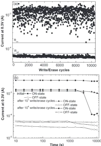
The electrical pulse-induced resistance change effect was also performed in Ti/ZrO2/Pt device (Fig. 4). After adding a
−3-V 10-µs voltage pulse on the device, the state is switched
toOFF-state and measured at 0.3 V. Then, adding a+6-V 10-µs voltage pulse on the device, theOFF-state is changed toON-state
368 IEEE ELECTRON DEVICE LETTERS, VOL. 28, NO. 5, MAY 2007
Fig. 4. (a) Dynamic pulse resistive switching of a Ti/ZrO2/Pt device for a “write-read-erase-read” sequence over 104cycles. (b) Nondestructive readout properties of a Ti/ZrO2/Pt device. Before 104write/erase cycles, bothON-state andOFF-state are kept stable. However, it shows a little drop ofRONafter 104 write/erase cycles.
is the same as that of the dc voltage sweeping operation. The write/erase operation indicated in Fig. 4(a) demonstrates that the device can be switched over 104cycles without degradation. Fig. 4(b) depicts the stability of the Ti/ZrO2/Pt device under
an ongoing bias voltage of 0.3 V after 103and 104write/erase cycles. The initialON-state andOFF-state are kept stable more than 104 s, indicating that the resistance states are not varied during 1012 read pulses (10 ns). Even after 103 write/erase cycles, both ON-state and OFF-state are almost kept at the same current values. Therefore, important properties of nonde-structive readout and good reliability are demonstrated in this device. However, after 104write/erase cycles, the current of the
ON-state shows a little drop, but remains higher than that of the
OFF-state, which would not cause a readout hazard.
However, there are various remaining questions needed to be studied, such as the possibility of oxidation of top elec-trode, nanodomain switch, conduction paths formation in the Ti/ZrO2/Pt device, to provide more detailed explanations about
why the Ti/ZrO2/Pt device exhibits better resistive switching
characteristics.
IV. CONCLUSION
The effect of the top electrode material on the switching behaviors of ZrO2 film memory devices was investigated. It was found that the Ti/ZrO2/Pt device exhibited better resis-tive switching properties in comparison with Pt/ZrO2/Pt and Al/ZrO2/Pt devices. It was demonstrated in the Ti/ZrO2/Pt device that it can be traced and reproduced over 1000 times with a little decrease of the resistance ratio between ON-state and
OFF-state. The dispersions of resistive switching parameters such as, RON, ROFF, VON, and VOFF, were minimized showing sharp distributions. The Ti/ZrO2/Pt device with the
write/erase operations over 104cycles without degradation and the good stability ofON-state andOFF-state has high potential for NVM applications.
REFERENCES
[1] C. Y. Liu, P. H. Wu, A. Wang, W. Y. Jang, J. C. Young, K. Y. Chiu, and T.-Y. Tseng, “Bistable resistive switching of a sputter-deposited Cr-doped SrZrO3 memory film,” IEEE Electron Device Lett., vol. 26, no. 6, pp. 351–353, Jun. 2005.
[2] W. W. Zhuang, W. Pan, D. B. Ulrich, J. J. Lee, L. Stecker, A. Burmaster, D. R. Evans, S. T. Hsu, M. Tajiri, A. Shimaoka, K. Inoue, T. Naka, N. Awaya, K. Sakiyama, Y. Wang, S. Q. Liu, N. J. Wu, and A. Ignatiev, “Novell colossal magnetoresistive thin film nonvolatile resistance random access memory (RRAM),” in IEDM Tech. Dig., 2004, pp. 193–196. [3] M. Fujimoto, H. Koyama, S. Kobayashi, Y. Tamai, N. Awaya,
Y. Nishi, and T. Suzuki, “Resistivity and resistive switching properties of Pr0.7Ca0.3MnO3thin films,” Appl. Phys. Lett., vol. 88, no. 24, p. 232 106, Dec. 2006.
[4] H. Sim, D. Choi, D. Lee, S. Seo, M. J. Lee, I. K. Yoo, and H. Hwang, “Resistance-switching characteristics of polycrystalline Nb2O5for non-volatile memory application,” IEEE Electron Device Lett., vol. 26, no. 5, pp. 292–294, May 2005.
[5] M. Fujimoto, H. Koyama, Y. Hosoi, K. Ishihara, and S. Kobayashi, “High-speed resistive switching of TiO2/TiN nano-crystalline thin film,” Jpn. J.
Appl. Phys., vol. 45, no. 11, pp. L310–L312, Mar. 2006.
[6] M. Fujimoto, H. Koyama, M. Konagai, Y. Hosoi, K. Ishihara, S. Ohnishi, and N. Awaya, “TiO2 anatase nanolayer on TiN thin film exhibiting high-speed bipolar resistive switching,” Appl. Phys. Lett., vol. 89, no. 22, p. 223 509, Nov. 2006.
[7] S. Seo, M. J. Lee, D. H. Seo, E. J. Jeoung, D.-S. Suh, Y. S. Joung, I. K. Yoo, I. R. Hwang, S. H. Kim, I. S. Byun, J.-S. Kim, J. S. Choi, and B. H. Park, “Reproducible resistance switching in polycrystalline NiO films,” Appl. Phys. Lett., vol. 85, no. 23, pp. 5655–5667, Dec. 2004. [8] D. Lee, H. Choi, H. Sim, D. Choi, H. Hwang, M. J. Lee, S. A. Seo, and
I. K. Yoo, “Resistive switching of the nonstoichiometric zirconium oxide for nonvolatile memory applications,” IEEE Electron Device Lett., vol. 26, no. 10, pp. 719–721, Oct. 2005.
[9] D. C. Kim, M. J. Lee, S. E. Ahn, S. Seo, J. C. Park, I. K. Yoo, I. G. Baek, H. J. Kim, E. K. Yim, J. E. Lee, S. O. Park, H. S. Sim, U.-I. Chung, J. T. Moon, and B. I. Ryu, “Improvement of resistive memory switch-ing in NiO usswitch-ing IrO2,” Appl. Phys. Lett., vol. 88, no. 23, p. 232 106, Jun. 2006.
[10] I. G. Baek, D. C. Kim, M. J. Lee, H. J. Kim, E. K. Yim, M. S. Lee, J. E. Lee, S. E. Ahn, S. Seo, J. H. Lee, J. C. Park, Y. K. Cha, S. O. Park, H. S. Kim, I. K. Yoo, U. I. Chung, J. T. Moon, and B. I. Ryu, “Multi-layer cross-point binary oxide resistive memory (OxRRAM) for post-NANDstorage application,” in IEDM Tech. Dig., 2005, pp. 750–753. [11] I. G. Baek, M. S. Lee, S. Seo, M. J. Lee, D. H. Seo, D. S. Suh, J. C. Park, H. S. Kim, I. K. Yoo, U. I. Chung, and J. T. Moon, “Highly scalable non-volatile resistive memory using simple binary oxide driven by asymmetric unipolar voltage pulses,” in IEDM Tech. Dig., 2004, pp. 587–590. [12] C. C. Lin, B. C. Tu, C. C. Lin, C. H. Lin, and T.-Y. Tseng, “Resistive
switching mechanisms of V-doped SrZrO3memory films,” IEEE Electron Device Lett., vol. 27, no. 9, pp. 725–727, Sep. 2006.