Improved reliability of Mo nanocrystal memory with ammonia plasma treatment
Chao-Cheng Lin, Ting-Chang Chang, Chun-Hao Tu, Wei-Ren Chen, Chih-Wei Hu, Simon M. Sze, Tseung-Yuen Tseng, Sheng-Chi Chen, and Jian-Yang Lin
Citation: Applied Physics Letters 94, 062106 (2009); doi: 10.1063/1.3081021 View online: http://dx.doi.org/10.1063/1.3081021
View Table of Contents: http://scitation.aip.org/content/aip/journal/apl/94/6?ver=pdfcov Published by the AIP Publishing
Articles you may be interested in
Effect of plasma treatment of resistive layer on a Cu/SiOx/Pt memory device J. Vac. Sci. Technol. A 32, 02B111 (2014); 10.1116/1.4859235
CF4 plasma treatment on nanostructure band engineered Gd2O3-nanocrystal nonvolatile memory J. Appl. Phys. 109, 064506 (2011); 10.1063/1.3556761
Passivated TiN nanocrystals/SiN trapping layer for enhanced erasing in nonvolatile memory Appl. Phys. Lett. 97, 152112 (2010); 10.1063/1.3501129
Performance and reliability improvement of HfSiON gate dielectrics using chlorine plasma treatment Appl. Phys. Lett. 94, 042911 (2009); 10.1063/1.3078277
Nonvolatile memory characteristics influenced by the different crystallization of Ni–Si and Ni–N nanocrystals Appl. Phys. Lett. 92, 062112 (2008); 10.1063/1.2841049
This article is copyrighted as indicated in the article. Reuse of AIP content is subject to the terms at: http://scitation.aip.org/termsconditions. Downloaded to IP: 140.113.38.11 On: Wed, 30 Apr 2014 15:30:27
Improved reliability of Mo nanocrystal memory with ammonia
plasma treatment
Chao-Cheng Lin,1Ting-Chang Chang,2,a兲 Chun-Hao Tu,1Wei-Ren Chen,1Chih-Wei Hu,1 Simon M. Sze,1Tseung-Yuen Tseng,1Sheng-Chi Chen,3and Jian-Yang Lin3
1
Institute of Electronics, National Chiao Tung University, Hsin-Chu 300, Taiwan
2
Department of Physics and Institute of Electro-Optical Engineering, Center for Nanoscience and Nanotechnology, National Sun Yat-Sen University, 70 Lien-hai Road, Kaohsiung 804, Taiwan
3
Department of Opto-Electronic Engineering, National Yunlin University of Science and Technology, Yunlin 64002, Taiwan
共Received 11 December 2008; accepted 23 January 2009; published online 12 February 2009兲 We investigated ammonia plasma treatment influence on the nonvolatile memory characteristics of the charge storage layer composed of Mo nanocrystals embedded in nonstoichiometry oxide共SiOx兲. X-ray photoelectron spectra analyses revealed that nitrogen was incorporated into the charge storage layer. Electric analyses indicated that the memory window was reduced and the retention and the endurance improved after the treatment. The reduction in the memory window and the improvement in retention were interpreted in terms of the nitrogen passivation of traps in the oxide around Mo nanocrystals. The robust endurance characteristic was attributed the improvement of the quality of the surrounding oxide by nitrogen passivation. © 2009 American Institute of Physics.
关DOI:10.1063/1.3081021兴
Nanocrystals embedded in dielectric as a charge storage layer of the floating gate structure attracted much attention for next generation nonvolatile memory. Employing discrete nanocrystals is expected to suppress charge loss due to lat-eral migration in poly-Si floating gate.1,2 Nanocrystals have been fabricated by several methods such as ion implantation,3,4sputtering,5,6and oxidation.7,8 It is expected that those processes can induce defects or traps in the oxide around nanocrystals during the fabrication process. The in-duced deficiency in the surrounding oxide can lead to stored charges leaking out of the nanocrystals through trap assisted tunneling.9,10Therefore, the quality of the surrounding oxide is an important issue to nanocrystal memory.
In this study, we investigated the effect of ammonia 共NH3兲 plasma treatment on memory characteristics of
Mo nanocrystal memory.11The NH3plasma treatment
tech-nique has been investigated to improve the quality of gate dielectric.12,13 Our experimental results show that the memory characteristics were influenced by incorporation of nitrogen into the surrounding oxide.
The memory cells were fabricated on 6 in. p-type Si substrate. After the substrate was cleaned with standard Ra-dio Corporation of America process, a 5-nm-thick dry oxide was thermally grown at 950 ° C on the substrate in a hori-zontal furnace. An 8-nm-thick Mo silicate layer was subse-quently deposited on the oxide layer by cosputtering Mo and Si in Ar 共24 SCCM兲/O 共2 SCCM兲 共SCCM denotes cubic centimeter per minute at STP兲 ambience. A 30-nm-thick Si oxide as the control oxide was deposited on the Mo silicate layer by plasma enhanced chemical vapor deposition 共PECVD兲 at 300 °C. Thermal annealing process was per-formed in N2ambience at 900 ° C at 60 s to form Mo
nano-crystals embedded in SiOx. Cells were then treated with NH3
plasma in PECVD chamber for 30 min with a NH3gas flow rate of 20 SCCM and the chamber pressure of 67 torr at
power of 50 W. To measure the electric characteristics, a 500-nm-thick Al was thermally evaporated through a shadow mask on the control oxide to form the metal-oxide-semiconductor 共MOS兲 structure. The x-ray photoemission spectroscopy 共XPS兲 was adopted to analyze the chemical bonding and composition of the charge storage layer. Elec-trical characteristics were measured using Keithley4200 and HP4284 Precision LCR meter.
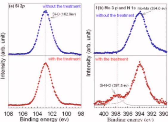
Figure 1 shows the XPS spectra of the charge storage layer with and without the plasma treatment, which was per-formed by using a monochromatic Al K␣共1486.6 eV兲 x-ray. Figure1共a兲shows the XPS Si 2p spectra of the charge stor-age for the sample with and without the plasma treatment. For the sample without the treatment in Fig. 1共a兲, the peak position of XPS Si 2p situated at 102.9 eV indicates that the surrounding oxide of nanocrystals is SiOx.14There is no ob-vious difference in the peak positions between the samples with and without the treatment. However, it was found that an additional XPS peak共397.8 eV兲 appears in the Mo 3p and N 1s spectra of the charge storage layer after the plasma treatment, which indicates that the incomplete bonds in SiOx
a兲Electronic mail: [email protected].
FIG. 1. 共Color online兲 共a兲 Si 2p, 共b兲 Mo 3p, and N 1s core-level spectra of the charge storage layer composed of Mo nanocrystals embedded in SiOx
with and without the plasma treatment.
APPLIED PHYSICS LETTERS 94, 062106共2009兲
0003-6951/2009/94共6兲/062106/3/$25.00 94, 062106-1 © 2009 American Institute of Physics
This article is copyrighted as indicated in the article. Reuse of AIP content is subject to the terms at: http://scitation.aip.org/termsconditions. Downloaded to IP: 140.113.38.11 On: Wed, 30 Apr 2014 15:30:27
bonded with nitrogen after the plasma treatment, as shown in Fig.1共b兲.15
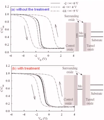
Figures 2共a兲 and 2共b兲 show the C-V curves of MOS structure embedded with Mo nanocrystals for the sample with and without the plasma treatment, respectively. At the smaller sweeping voltage of 2 V, there is a negligible memory window in Figs.2共a兲and2共b兲corresponding to the quasineutral state共i.e., no charge is stored in the charge stor-age layer under this sweeping range兲. At the larger sweeping voltages, there are counterclockwise memory hystereses in Fig. 2. The counterclockwise hystereses are due to carrier transport through tunnel oxide between the charge storage layer and the Si substrate. We note that the memory windows of the sample with the plasma treatment are smaller than that without the treatment. For the smaller memory window after the treatment, we speculate the nitrogen passivation in the charge storage layer. It has been suggested that the traps in the oxide around nanocrystals can capture carriers and con-tribute to the memory window.16,17 According XPS results,
the nitrogen was incorporated into the oxide around the Mo nanocrystals after the treatment. The incorporated nitrogen can passivate the traps in the oxide, which reduces the charge storage centers and leads to the smaller memory window, as indicated in the insets of Fig.2.
Figure3is the comparison of the retention behavior for the samples with and without the plasma treatment. The re-tention was measured by a stress voltage of 10 V on Al gate electrode for 5 s. The memory window was obtained by comparing the C-V curves after the programming to the quasineutral state. It can be found in Fig. 4 that, after the 103 s retention time, the decay rate共⫺66 mV/decade兲 of the
memory window for the sample with the plasma treatment is slower than that without the treatment 共⫺115 mV/decade兲. The superior retention of the sample with the treatment can be explained by the nitrogen passivation of the traps in the oxide around Mo nanocrystals. When charges are stored in the nanocrystals, the stored charges can escape with the as-sistance of traps 共traps assist tunneling兲 in the surrounding oxide. Because the traps in the oxide were reduced after the plasma treatment, the retention was improved by suppressing the trap assisted tunneling process.
Figures4共a兲and4共b兲 presents the endurance character-istics of the samples with and without plasma treatment un-der the pulse conditions of VG=⫾15 V for 1 ms, respec-tively. In Fig.4共a兲, the⌬VFB共the difference in VFBbetween
programming and erase states兲 reduced significantly, and the ⌬VFB remained 51% after 106 program/erase cycles.
How-ever, the plasma treated sample exhibits robust endurance characteristic共⌬VFBof 89% after 106program/erase cycles兲.
It is known that the⌬VFBreduction during the endurance test is due to the degradation of the gate oxide.18The better en-durance characteristics of the sample with the plasma treat-ment can be attributed to the improvetreat-ment of quality of the surrounding oxide. During the endurance test, the carriers transport between nanocrystals and the substrate can damage the surrounding oxide, which produces more traps. Because the surrounding oxide was strengthened by the nitrogen in-corporation after the treatment, the generation rate of traps reduced, resulting in the better endurance characteristic.
In conclusion, the nonvolatile memory characteristics of the Mo nanocrystals were influenced by the ammonia plasma treatment. The C-V hysteresis reduced to 3.0 V and retention characteristic improved with decay rate of ⫺66 mV/decade after the plasma treatment due to the nitrogen passivation of the traps in the oxide around the nanocrystals. The incorpo-ration of nitrogen into the charge storage layer through the NH3 plasma treatment can strengthen the endurance
charac-teristic of Mo nanocrystals memory. FIG. 3. 共Color online兲 The retention behavior of the MOS structures with
and without the plasma treatment.
FIG. 4. 共Color online兲 Endurance characteristic of the MOS structures 共a兲 with and共b兲 without the plasma treatment.
FIG. 2. 共Color online兲 C-V curves of the MOS structure with and without the plasma treatment. The inset of the is the simple band diagram of the structure in the flat-band state.
062106-2 Lin et al. Appl. Phys. Lett. 94, 062106共2009兲
This article is copyrighted as indicated in the article. Reuse of AIP content is subject to the terms at: http://scitation.aip.org/termsconditions. Downloaded to IP: 140.113.38.11 On: Wed, 30 Apr 2014 15:30:27
This work was performed at the National Nano Device Laboratories, Taiwan, R.O.C. The authors acknowledge the financial support of the National Science Council共NSC兲 un-der Contract Nos. NSC 2221-E-009-202-MY3, NSC 96-2112-M-110-013, and NSC-97-3114-M-110-001.
1S. Tiwari, F. Rana, K. Chan, H. Hanafi, W. Chan, and D. Buchanan, Tech.
Dig.-Int. Electron Devices Meet 1995, 521.
2Y. Liu, S. Tang, and S. K. Banerjee,Appl. Phys. Lett. 88, 213504共2006兲. 3Y.-C. King, T.-J. King, and C. Hu,IEEE Trans. Electron Devices 48, 696
共2001兲.
4C. Y. Ng, T. P. Chen, L. Ding, M. Yang, J. I. Wong, P. Zhao, X. H. Yang,
K. Y. Liu, M. S. Tse, A. D. Trigg, and S. Fung,IEEE Trans. Electron Devices 53, 730共2006兲.
5V. Ho, L. W. Teo, W. K. Choi, W. K. Chim, M. S. Tay, D. A. Antoniadis,
E. A. Fitzgerald, A. Y. Du, C. H. Tung, R. Liu, and A. T. S. Wee,Appl. Phys. Lett. 83, 3558共2003兲.
6K. I. Han, Y. M. Park, S. Kim, S. H. Choi, K. J. Kim, I. H. Park, and B. G.
Park,IEEE Trans. Electron Devices 54, 359共2007兲.
7L. W. Teo, W. K. Choi, W. K. Chim, V. Ho, C. M. Moey, M. S. Tay, C. L.
Heng, Y. Lei, D. A. Antoniadis, and E. A. Fitzgerald,Appl. Phys. Lett. 81,
3639共2002兲.
8J. K. Kim, H. J. Cheong, Y. Kim, J. Yi, H. J. Bark, S. H. Bang, and J. H.
Cho,Appl. Phys. Lett. 82, 2527共2003兲.
9M. Houssa, M. Tuominen, M. Naili, V. Afanas’ev, A. Stesmans, S.
Haukka, and M. M. Heyns,J. Appl. Phys. 87, 8615共2000兲.
10W. R. Chen, T. C. Chang, P. T. Liu, P. S. Lin, C. H. Tu, and C. Y. Chang,
Appl. Phys. Lett. 90, 112108共2007兲.
11C. C. Lin, T. C. Chang, C. H. Tu, W. R. Chen, C. W. Hu, S. M. Sze, T. Y.
Tseng, S. C. Chen, and J. Y. Lin,Appl. Phys. Lett. 93, 222101共2008兲.
12X. Zeng, X. W. Sun, J. Li, and J. K. O. Sin,Microelectron. Reliab. 44,
435共2004兲.
13J. R. Shallenberger, D. A. Cole, and S. W. Novak,J. Vac. Sci. Technol. A
17, 1086共1999兲.
14B. Gallas, C. C. Kao, S. Fisson, G. Vuye, J. Rivory, Y. Bernard, and C.
Belouet,Appl. Surf. Sci. 185, 317共2002兲.
15Z. H. Lu, S. P. Tay, R. Cao, and P. Pianetta,Appl. Phys. Lett. 67, 2836
共1995兲.
16C. Busseret, A. Souifi, T. Baron, S. Monfray, N. Buffet, E. Gautier, and M.
N. Semeria,Mater. Sci. Eng., C 19, 237共2002兲.
17W. R. Chen, T. C. Chang, J. L. Yeh, S. M. Sze, C. Y. Chang, and U. S.
Chen,Appl. Phys. Lett. 91, 222105共2007兲.
18P. Pavan, R. Bez, P. Olivo, and E. Zanoni,Proc. IEEE 85, 1248共1997兲.
062106-3 Lin et al. Appl. Phys. Lett. 94, 062106共2009兲
This article is copyrighted as indicated in the article. Reuse of AIP content is subject to the terms at: http://scitation.aip.org/termsconditions. Downloaded to IP: 140.113.38.11 On: Wed, 30 Apr 2014 15:30:27