Chemically Doped and Cross-linked Hole-Transporting Materials as
an Efficient Anode Buffer Layer for Polymer Solar Cells
Ying Sun,
†,‡Shang-Chieh Chien,
†,§Hin-Lap Yip,
†Yong Zhang,
†Kung-Shih Chen,
†David F. Zeigler,
⊥Fang-Chung Chen,
§Baoping Lin,*
,‡and Alex K.-Y. Jen*
,††Department of Materials Science and Engineering, University of Washington, Seattle, Washington, United States
‡School of Chemistry and Chemical Engineering, Southeast University, Jiangning District, Nanjing, Jiangsu Province, P.R. China §Department of Photonics & Display Institute, National Chiao Tung University, Hsinchu 30010, Taiwan
⊥Department of Chemistry, University of Washington, P.O. Box 351700, Seattle, Washington 98195, United States
*
S Supporting InformationABSTRACT: A series of cross-linkable hole-transporting materials (X-HTMs) consisting of indacenodithiophene, bithiophene, and thiophene units bookended by two triaryl-amine groups have been designed and synthesized to investigate their suitability as new anode buffer layer for bulk heterojunction polymer solar cells (PSCs). These X-HTMs can be thermally cross-linked at temperature between 150 and 180 °C to form robust, solvent-resistant films for subsequent
spin-coating of another upper layer. Energy levels of these cross-linked materials were measured by cyclic voltammetry, and the data suggest that these X-HTMs have desirable hole-collecting and electron-blocking abilities to function as an anode buffer layer for PSCs. In addition, by incorporating thiophene or fused ring units into the X-HTM backbone, it effectively improved the hole-carrier motilities. To further improve the conductivity and optical transparency for PSCs, the X-HTM films were p-doped with nitrosonium hexafluoroantimonate (NOSbF6). The doped X-HTM layers showed remarkably enhanced hole-current densities
compared to neutral X-HTM under the same electric field bias. The properties of the doped X-HTM film as anode buffer layer has been investigated in PSCs. The resulting devices showed similar performance compared to those made using conducting polymer, poly(3,4-ethylene- dioxylenethiophene):poly(styrenesulfonate) (PEDOT:PSS), as the anode buffer layer. Moreover, a novel bilayer HTM structure consisting of a doped and a neutral layer was employed to exploit the feasibility of combining high conductivity from the doped X-HTM and good electron-blocking ability from the neutral X-HTM together. Interestingly, PSC devices based on this bilayer structure showed enhanced Voc, Jsc, and FF compared to the devices with only a single-layer doped
X-HTM. These results indicate that such X-HTMs are promising alternative materials to PEDOT:PSS as an anode buffer layer for polymer solar cells.
KEYWORDS: hole-transporting materials, cross-linking, PEDOT:PSS, anode buffer layer, doping, polymer solar cells
1. INTRODUCTION
Polymeric solar cells (PSCs) have emerged as a promising source of alternative energy because of their flexibility, light weight, and the potential of using roll-to-roll processing to produce low cost solar cells. In general, a PSC consists of a bulk heterojunction (BHJ) photoactive layer in which the p-type polymer donor and n-type electron acceptor can form a bicontinuous interpenetrating network.1−5 Currently, the record of power conversion efficiency (PCE) of a single-junction PSC has exceeded 7%.6−10
In most PSCs, the conducting polymer, poly(3,4-ethylene-dioxylenethiophene):poly(styrenesulfonate) (PEDOT:PSS) is often used as an anode buffer layer between the indium tin oxide (ITO) substrate and the BHJ layer to facilitate hole-collection/extraction11and improve the surface quality of ITO to prevent short circuits.12Due to its high work function (5.0− 5.2 eV), PEDOT:PSS helps form Ohmic contact with the BHJ to improve the open-circuit voltage (Voc) and charge-collecting
ability of PSCs.13 However, the relatively high acidity of PEDOT:PSS (pH ∼ 1) tends to corrode ITO and cause the loss of indium, resulting in device degradation.14,15In addition, the electrical inhomogeneity and varying morphology of the PEDOT:PSS film16,17 combining with its poor electron-blocking capability18limit its application in PSCs.19For these reasons, several interfacial layer materials have been explored to replace PEDOT:PSS.14,20−26 Recently, a copolymer based on grafting poly(styrenesulfonate) on polyaniline (PSSA-g-PANI) has been employed as the hole-collecting anode buffer layer in PSCs combining both good electrochemical stability and excellent water solubility on the same material.23 The PSCs using this copolymer as the interfacial layer exhibited higher Jsc
and PCE compared to those using PEDOT:PSS because of its Received: August 15, 2011
Revised: October 9, 2011 Published: October 25, 2011
improved optical transparency and electrical conductivity. Hains et al.20,21have recently also tried to replace PEDOT:PSS by cross-linking the blend of poly[(9,9-dioctylfluorene)-co-N-[(4-(3-methylpropyl)] diphenyl amine] (TFB) and 4,4-bis[(p-trichlorosilylpropylphenyl) phenylamino] biphenyl (TPDSi2).
Solar cells made with this anode buffer layer also showed improved performance and thermal stability over those using PEDOT:PSS in the devices. These encouraging results showed that new interfacial materials deserve further investigation in order to improve their properties.
To be a suitable anode buffer layer for PSC, a material must meet several requirements. First, it should have adequate solvent resistance to allow subsequent solution processing of the upper BHJ layer. Second, its highest occupied molecular orbital (HOMO) level should be at or slightly above that of the donor material in the BHJ layer to facilitate hole collection. Third, its lowest unoccupied molecular orbital (LUMO) level should be high enough to block electrons.22Finally, it should have good electrical conductivity and optical transparency throughout the visible region of the spectrum.
Triarylamine (TAA) derivatives, such as N,N′-bis(tolyl)-N,N′-diphenyl-1,1′-biphenyl-4,4′-diamine (TPD), are commonly used as efficient hole-transporting materials (HTMs) due to their low ionization potential and good electron-blocking character-istics.27−30 However, these materials possess relatively low hole-mobilities31 due to their short conjugation length and amorphous nature. Conversely, thiophene derivatives have been incorporated into p-type polymer to improve hole-mobility due to their better planarity and electron richness.32−35Therefore, it is expected that the incorporation of thiophene analogues should increase mobility of the TAA-based HTMs. Further-more, if these materials can be doped, it may simultaneously improve their conductivity and Ohmic contact as has been successful demonstrated for organic light-emitting diodes.36−42
Motivated by these results, we have designed and prepared a series of cross-linkable hole-transporting materials (X-HTMs) by combining triphenylamine with indacenodithiophene (IDT), bithiophene, and thiophene units. Bearing styryl groups, the resulting HTMs can be thermally cross-linked at temper-ature around 150−180 °C to form robust layers for the sub-sequent spin-coating of active layer. The mobility of X-HTM derived from cross-linking these materials were determined by the space-charge-limited-current (SCLC) method in the hole-only device configuration. It is found that the introduction of thiophene derivatives into the main chain of X-HTM effectively increases their carrier mobility.
In order to improve their conductivity and optical trans-parency, the X-HTLs were doped with a strong oxidant, NOSbF6. After doping, the absorption spectra of the X-HTLs
red-shifted to the near infrared (NIR) region to provide better optical transparency in the visible region, while the doped X-HTLs still maintained good solvent resistance. Hole-only devices derived from these doped X-HTLs showed significantly enhanced hole-current density under the same electric field compared to those derived from neutral X-HTL. With these combined desirable properties, the doped X-HTLs have been applied as the anode buffer layer in PSCs. The derived devices gave significantly enhanced Voc, Jsc, and FF values than those
without a HTL. Furthermore, the PSC with a bilayer device structure consisting of a doped X-HTL and a neutral X-HTL underneath has been utilized to combine Ohmic contact and efficient hole-transporting and electron-blocking properties
simultaneously. A significantly improved device performance can be achieved from using this hybrid bilayer structure.
2. RESULTS AND DISCUSSION
2.1. Synthesis. The molecular structures of X-HTMs studied in this paper are shown in Scheme 1. All the HTMs
are designed to have the linker of dimethylene ether group (CH2−O−CH2) to provide adequate flexibility for the styryl
groups to react with each other in solid-state. The bulky
n-butyl-phenyl chains were introduced to the IDT unit of
IDT-BTPA to help reduce rigidity of the backbone and lower the cross-linking temperature.
The synthetic routes for HTMs are depicted in Scheme 2. Initially, 4-methyltriphenylamine was prepared via a
palladium-catalyzed Buchwald−Hartwig cross-coupling reaction between diphenylamine and 4-iodotoluene. Boronic ester compound 3 was obtained by monobrominating 4-methyltriphenylamine in a one-pot synthesis to afford 2 in 58% yield. Compound 4 was synthesized by following the reported procedure43through the addition of 1-hexylbenzene lithium into the solution containing the ester to give the corresponding alcohol and then cyclized subsequently through the acid-mediated reaction. The dibromo IDT compound 1a was synthesized by bromonating compound 4 using N-bromo succinic imide (NBS).
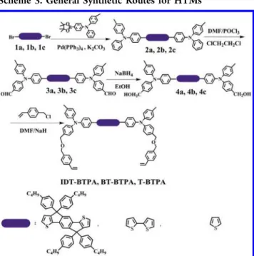
Scheme 3 illustrates the procedures used for preparing the X-HTMs. The Suzuki coupling reaction between the boronic ester 3 and the corresponding dibromo compounds (1a, 1b, 1c) afforded compounds 2a, 2b, and 2c. The compounds were then diformylated through the Vilsmeier reaction using POCl3/DMF in dicholoethane to give compounds 3a, 3b, and
3c in ∼70% yield. Reduction of 3a, 3b, and 3c with sodium Scheme 1. Chemical Structures of HTMs
Scheme 2. Synthetic Routes of Backbone Compounds for HTMs
borohydride in ethanol/THF yielded the corresponding hydroxyl compounds (4a, 4b, 4c), which were then treated with NaH and 4-vinylbenzyl chloride to afford the final products, IDT-BTPA, BT-BTPA, and T-BTPA. The structure and purity of these HTM precursors were confirmed by1H NMR,13C NMR, and HRMS
(ESI).
The resulting X-HTMs precursors were very soluble in common organic solvents including THF, CHCl3, acetone,
chlorobenzene, and dichlorobenzene at room temperature. The good solubility allows the HTMs to be easily solution processed to obtain films with tunable thicknesses.
2.2. Thermal Cross-Linking and Optical Properties. The styrene groups on the HTM precursors was used for cross-linking to facilitate thermal-induced polymerization without using any initiator.44To investigate thermal cross-linking of the HTMs, differential scanning calorimetry (DSC) experiments were conducted, and the results are shown in Figure 1. The broad exothermic peaks between 90 and 190 °C in the first scan indicated the thermal-initiated polymerization of the styrene groups. No obvious exothermic peaks can be observed in the second heating of each HTM, indicating the completeness of the cross-linking reaction after the first heating cycle. In addition, there is no Tgor melting point that can be observed
during the second heating, which suggests that these cross-linked HTMs possess good morphological stability.
The higher Tmaxvaleus of IDT-BTPA (∼172 °C) and BT-BTPA
(∼166 °C) are consistent with their more rigid backbones compared to T-BTPA (∼158 °C) and 1-TPD (∼136 °C). With increased backbone rigidity, it becomes more difficult for the styrene groups to encounter each other. Thus, cross-linking reaction of the more rigid systems needs higher temperatures and longer time to complete.
Solvent resistance of these HTM was studied by monitoring the UV/vis spectrum of each cross-linked film before and after rinsing with chlorobenzene (CB), which is the commonly used solvent for device processing (Figure 1). The X-HTM film was spin-coated from its chloroform solution (5 mg/mL) onto an ITO substrate and thermally cross-linked in a nitrogen-filled
glovebox. The annealing temperature and time for each HTM are listed in Table 1. After curing at 180 °C for 1 h, the
IDT-BTPA film exhibited a slight drop-off in the intensity of its absorption λmax after rinsing with CB. However, the
cross-linked BT-BTPA and T-BTPA films showed excellent solvent resistance evidenced by identical absorption spectra before and after rinsing. This good solvent resistance allows the subsequent spin-coating to be performed on top of the HTL without eroding it. All the X-HTMs showed absorption in the range of below 500 nm, suggesting that they have minimal interference with the absorbance of many low bandgap polymers (Figure S1 of the Supporting Information). The main peak at the longer wavelength can be ascribed to the
π−π* transition derived from the conjugation chain. So
red-shift in the absorption peak can be observed with the increasing Scheme 3. General Synthetic Routes for HTMs
Figure 1. DSC curves of HTMs in the first and the second heating circle and UV−vis absorption spectrum of X-HTM before rinsing and after rinsing with chlorobenzene.
Table 1. Thermal Cross-Linking Conditions and Electrical Properties for HTMs (X-T: Cross-Linking Temperature; X-time: Cross-Linking Time)
HTM (°C)X-T time(min)X- (nm)λonset (eV)Eg HOMO(eV) LUMO(eV)
1-TPD 150 30 409.4 3.03 −5.25 −2.22
T-BTPA 160 30 453.5 2.73 −5.15 −2.42
BT-BTPA 180 30 497.7 2.49 −5.08 −2.59
number of thiophene units in the X-HTMs due to the extended conjugation length from 406 nm for T-BTPA to 431 nm for BT- BTPA and 445 nm for IDT-BTPA. A shoulder peak appearing in the absorption of IDT-BTPA indicates good packing of the polymer chain in the film. The bandgaps of the HTMs were calculated from the absorption onset (λonset) and
listed in Table 1.
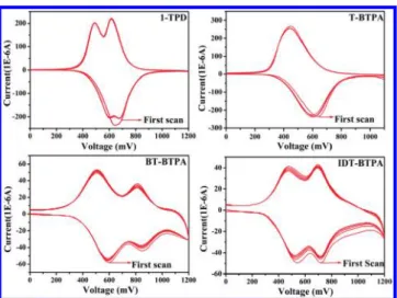
2.3. Electrochemical Properties. The electrochemical properties of cross-linked HTMs were investigated by using cyclic voltammetry (CV) (Figure 2). The CV potentials were
measured using ITO substrates as the working electrode and a Ag/AgCl reference electrode in acetonitrile with 0.1 M of tetrabutylammonium hexafluorophosphate. The obtained results were calibrated using a ferrocene/ferrocenium redox couple. There were two reversible oxidation redox couples with cathodic peak potentials (Epc) of 0.47 and 0.69 V for IDT-BTPA and 0.51
and 0.81 V for BT-BTPA but only one couple at 0.45 V (Epc)
for T-BTPA. For comparison, the electrochemical behavior of 1-TPD was also investigated. For 1-TPD, two peaks always appeared during the cathodic sweep while the first and second peaks in the anodic sweep overlapped with each other.
There have been numerous studies for the electrochemical properties of triphenylamine derivatives due to their applica-tions in organic electronics.45−48 It was found that multiple oxidation peaks appeared when the coupling between the redox centers was strong and electrons were delocalized throughout the entire system. On the contrary, these oxidative peaks overlapped completely when the interactions between localized redox centers were weak.49,50 Therefore, the single oxidation redox couple for T-BTPA may be due to the weaker electronic coupling between two redox amino centers as a result of the insertion of a thiophene spacer compared to 1-TPD. However, for IDT-BTPA and BT-BTPA, the other amine probably cannot be readily oxidized after the formation of one amino redox center due to the increased spacer, more rigid bithiophene, IDT units, and the two oxidative peaks probably due to the two successive electron removal processes.50
The first oxidation potentials of IDT-BTPA and BT-BTPA were lower than that of T-BTPA, which may be attributed to the increased electron density in their backbones as more electron-rich IDT and bithiphene units were introduced. The cyclic voltammograms showed minimal changes after ten cycles, indicating all these X-HTMs have very good
electrochemical stability. The energy levels of HTMs are summarized in Table 1. The highest occupied molecular orbital (HOMO) energy level was calculated from the onset of oxidation potentials (Eox) using the equation of HOMO =
−[Eox+ 4.80] eV. The lowest unoccupied molecular orbital
(LUMO) energy level of each HTM was obtained from the difference between the bandgap and the HOMO energy level of the HTM. The HOMO energy levels of the X-HTMs are ranging from −5.06 to −5.15 eV, which is suitable for hole-collection for most of the donor polymers in PSCs. In addition, the higher LUMO energy level (−2.42 to −2.58 eV) of the X-HTMs suggests that they can provide good electron blocking as the anode buffer layer in the PSCs.
2.4. Doping Properties. To improve conductivity of X-HTMs, we have performed p-doping on X-HTLs using a strong oxidant, NOSbF6, as dopant in the solvent of acetonitrile.
Upon doping, electrons were transferred from the HTM to reduce NO+ and form NO as gas, which can be subsequently
released. The positive charge carriers will be formed on the HTM chain with SbF6−as the counterion.
Different UV−vis absorption spectra of the HTMs under different doping states were monitored and shown in Figure 3.
The HTMs exhibited absorption between 300 and 500 nm and were transparent in the NIR region in their neutral form as mentioned before. Take 1-TPD as an example, in the initial stage of the doping experiment, the intensity of the original absorption peak decreased with the formation of new absorption peaks at about 500 nm and another broad absorption band (1000−2000 nm) appeared in the NIR region. The formation of a monocation radical (polaron charge carrier) leads to the new red-shifted absorption peak of ∼500 nm while the new absorption band in the NIR region is due to the intervalence charge transfer (IV-CT) between nonequivalent states related to the positive charges in different amino centers.51Upon further doping, the polaron and IV-CT absorption band decreased gradually while another new broad band grow up at about 600− 1000 nm which is due to the formation of a dication (bipolaron charge carrier).52 At the fully doped state, the previous π−π* peak (350 nm) disappeared while the main absorption is from the bipolaron band. For the other three HTMs, the similar trend Figure 2. Cyclic voltammograms of HTMs (scan rate: 100 mV/s).
Figure 3. UV−vis absorption of the HTMs at different doping stages. Dopant concentration: 1-TPD 0.5 mg/mL, IDT-BTPA 0.2 mg/mL, BT-BTPA 0.5 mg/mL, T-BTPA 0.5 mg/mL; rinsing solvent: chlorobenzene.
of the UV−vis absorption change can be observed at different doping stages with obvious color change that can be observed by naked eye.
However, for different HTMs to be fully doped, the required dopant concentration and time varied due to the possibility for charge transfer and the diffusivity of the dopant in the matrix films. The lower dopant concentration required to fully dope the IDT-BTPA film may be related to its stronger electron-donating ability and better diffusion of NOSbF6 due to the
relatively loosely packed film resulting from the branched alkyl chains on the backbone.
For IDT-BTPA and BT-BTPA, the main absorption bands were located in the NIR region when they were fully doped, which provided good optical transparency with minimal absorption loss of the active light-harvesting layer. Moreover, significant increase in charge carrier density in the fully doped form can result in high conductivity, which is important to the reduction of Ohmic loss at the hole-collection contact. It is worthy to mention that the absorption spectra of the doped HTM films remained similar after washing several times with CB. This indicated that the doped X-HTLs possess good solvent resistance which is critical to multilayer solution processing of PSCs.
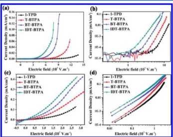
2.5. Charge-Transporting Properties. In order to investigate the hole-transporting properties of the HTMs, hole-only devices were fabricated with the configuration of ITO/PEDOT:PSS(40 nm)/HTM/MoO3/Al.53Figure 4 shows
the current density−electric field (J−E) curves of these hole-only devices in linear-representing and log−log plots measured in a dark environment. As observed in J−E curves, these newly developed HTMs (IDT-BTPA, BT-BTPA, and T-BTPA) exhibit comparatively higher current density compared to that of 1-TPD under the same electric field bias. From earlier studies, the IDT-based alternating copolymers were reported to exhibit remarkable hole-mobility (up to 1.0 cm2/V·s) due
to their coplanar structure and strong intermolecular π−π interactions.54−58 As expect, IDT-BTPA showed the best hole-transporting property while BT-BTPA incorporating a bithio-phene unit had better hole-transporting properties than T-BTPA, which has only a single thiophene ring.
One of the critical factors for material to be used as an anode buffer layer in OPV is the electrical conductivity, which will affect both the Ohmic contact at the electrode and the electrical resistance across the device. To investigate the doping effect on the conductivity, hole-only devices incorporating doped HTLs were fabricated. As shown in Figure 4c and d, the same trend can be observed for four different doped HTLs. Significantly higher current density can be obtained via doping compared to the neutral HTLs. At the electrical field of 1 V/m, the current density increased from 10−5−10−4 mA/cm2 for the neutral
HTLs to the range of 10−2−10−1mA/cm2for the doped HTLs.
These results revealed the pronounced effects of doping on hole-transporting properties of HTLs due to increased charge carrier number density and conductivity. The charge mobility of HTMs were extracted by fitting the log−log current density−voltage (J−V) curves and employing the SCLC equation of J = 9ε0εrμV2/8L3, where J is the current density
(mA/cm2), ε
0εris the permittivity of HTM, μ is the mobility,
and L is the thickness of the HTL. The mobility of the X-HTMs increased with more thiophene or fused rings introduced onto the backbone of the X-HTMs. The hole-mobility of IDT-BTPA was determined to be 1.26 ± 0.14 × 10⁻⁴cm2/V·s which is much higher than that of 1-TPD (6.35 ±
0.32 × 10⁻⁶ cm2/V·s). BT-BTPA also exhibited a higher mobility (6.29 ± 0.73 × 10⁻⁵cm2/V·s) compared to T-BTPA
(2.03 ± 0.25 × 10⁻⁵cm2/(V·s). The increase of mobility can be explained by the more rigid and planar structure as well as strong intermolecular π−π interactions.
2.6. Interfacial Properties as the Anode Buffer Layer in Photovoltaic Cells. To evaluate the suitability of these newly developed HTMs to function as an anode buffer layer, PSCs solar cells were first fabricated with the configuration of ITO/HTL/polymer:PC71BM/Ca/Al, where a low bandgap
copolymer PIDTPhTQ was selected as the p-type donor and PC71BM was chosen as the acceptor (Figure 5).59IDT-BTPA
and BT-BTPA were selected for study due to their superior charge-transporting abilities over T-BTPA and 1-TPD. For comparison, typical devices with bare ITO and PEDOT:PSS were also fabricated in parallel. The detailed fabrication process is depicted in the Experimental Section. The detailed device results based on various anode buffer layers with different thicknesses are listed in Table 2, and the representative J−V Figure 4. Current density−electric field (J−E) curves of the hole-only
devices incorporating various HTMs without doping (a and b) and with doping (c and d) in linear (a and c) and log−log (b and d) plots.
Figure 5. Chemical structure of the active polymer and OPV device architecture with different anode buffer layer (without buffer layer; PEDOT:PSS; single doped layer; bilayer).
curves of the optimized devices for each HTL are shown in Figure 6. The device without any buffer layer showed poor
performance with relatively low Voc(0.42 V), FF (45%), and
PCE (1.56%). In this case, the inferior Vocmay be determined
by the anode−cathode work function differential instead of the difference between the HOMO level of the polymer and the LUMO level of PC71BM, which indicated the poor contact
between the bare ITO and BHJ layers. Upon addition of the doped HTL (IDT-BTPA or BT-BTPA), the devices gave rise to significantly improved Voc as well as higher Jsc and FF. The
obviously enhanced performance of the device after incorporat-ing doped HTLs represented that the X-HTLs can effectively create Ohmic contact at the anode side for achieving higher Voc
and facilitating charge collection to give higher Jsc. Moreover,
the doping processes potentially induce the gradual shift of the HTM Fermi level toward its HOMO level and therefore reduce interface energy barrier.40
Since the film morphology of the anode buffer layer is very crucial for PSC application because slight defects such as aggregates or pinholes can easily diminish device performance, atomic force microscopy (AFM) was employed to investigate the surface morphology of the X-HTLs film. As shown in Figure 7, the HTMs form smooth and uniform films on ITO substrates with the rms roughness of 0.67 and 0.48 nm for IDT-BTPA and BT-IDT-BTPA, respectively. Therefore, the X-HTL can effectively suppress the formation of uneven morphology due to the rough ITO surface (rms: 2.41 nm)60 and enable the active layer to achieve optimal morphology. The morphology of the blend of polymer and PC71BM on the doped HTL was also
investigated by AFM. The photoactive layer film exhibited a smooth surface with roughness of ca. 1.29 and 1.28 nm on the doped IDT-BTPA and BT-BTPA layer, respectively, and no obvious phase separation can be observed.
Thickness is another critical factor for functioning as buffer layers since it can influence the electrical characteristics of OPVs. Therefore, we also investigated the dependence of doped HTL thickness on device performance. The summarized device performance is shown in Table 2. It can be seen that IDT-BTPA showed minor effect of thickness variation on the device performance while thickness has a huge effect on the device characters for BT-BTPA. Thicker HTL induced poorer device performance. Since equal dopant concentration and time were used to dope HTL with different thicknesses, these phenomena can be attributed to the comparatively different doping degree in the HTL applied to the device. As previously mentioned, IDT-BTPA can be readily doped; therefore, even thicker film can be fully doped to reach the required conductivity for efficient charge transport. However, BT-BTPA is more difficult to fully dope; thereby a thick film may remain with low conductivity at the interface between the active layer and HTL to inhibit the efficient charge transport. In addition, the inferior hole-transporting ability of the BT-BTPA Table 2. Photovoltaic Properties of Polymer Solar Cells Incorporating Different Anode Buffer Layers with Different Thicknessesa
Active Polymer Anode Buffer Layer Voc(V) Jsc(mA/cm2) FF (%) PCE (%) SD (%)
PIDTPhTQ bare ITO 0.42 8.27 45.0 1.56 0.21
PIDTPhTQ PEDOT:PSS 0.81 10.09 56.0 4.58 0.15
PIDTPhTQ doped BT-BTPA (7 nm) 0.80 9.40 49.2 3.70 0.31
PIDTPhTQ doped BT-BTPA (15 nm) 0.75 7.48 47.2 2.65 0.25
PIDTPhTQ doped BT-BTPA (20 nm) 0.57 2.89 52.6 0.86 0.22
PIDTPhTQ doped IDT-BTPA (7 nm) 0.77 9.74 52.6 3.94 0.37
PIDTPhTQ doped IDT-BTPA (15 nm) 0.79 9.66 49.1 3.73 0.32
PIDTPhTQ doped IDT-BTPA (20 nm) 0.79 9.51 50.3 3.80 0.32
PIDTPhTQ bilayer 0.81 10.08 55.5 4.53 0.15
PIDTPhanQ PEDOT:PSS 0.85 10.74 61.0 5.55 0.16
PIDTPhanQ bilayer 0.85 9.53 66.0 5.32 0.17
a
Bilayer: BT-BTPA (7 nm)/doped IDT-BTPA (20 nm). SD standard deviation.
Figure 6. (a) Current density−voltage (J−V) curves. (b) Dark current characteristics of the photovoltaic devices incorporating various anode buffer layers. (Device configuration): ITO/HTL/PIDTPhTQ:PC71BM (1:3)/Ca/Al.
Figure 7. AFM images (5 μm × 5 μm) for the IDT-BTPA (a), X-BT-BTPA (b) layer and the active layer of PIDTPhTQ: PC71BM (1:3) on doped X-IDT-BTPA (c) and X-BT-BTPA (d).
may cause it to be more dependent on the thickness of the HTL compared to the IDT-BTPA.
In addition to device performance, a more detailed understanding of the function of HTMs was realized by investigating the J−V curves of the devices measured in the dark (Figure 6b). Surprisingly, the device incorporating doped HTMs featured serious leakage current under reverse-bias and small forward-bias, although the injection (forward-bias from 1 to 2 V) showed comparable carrier injection ability compared to the device based on PEDOT:PSS as a buffer layer. This leakage current causes the device to have lower FF and Jsc. We
speculate that the thin, doped HTLs behave more metallic-like property than the semiconducting property. The semiconduct-ing, neutral form HTL is critical for providing better-defined energy bands to improve charge blocking effect.61In order to further improve the electron-blocking properties of these HTMs, a bilayer structure with the doped IDT-BTPA layer on top of the neutral BT-BTPA layer was introduced as the hybrid HTL system in the devices. Since BT-BTPA requires much higher dopant concentration than that for IDT-BTPA, the IDT-BTPA can be fully doped while controlling BT-BTPA to remain neutral through the manipulation of the dopant concentration. As shown in Figure S2 (in the Supporting Information), the original absorption peak of the bottom BT-BTPA in the bilayer structure remained the same, while the upper IDT-BTPA layer was fully doped. The fully doping of IDT-BTPA was confirmed by comparing its NIR absorption with that of the doped single layer IDT-BTPA. Therefore, the doped IDT-BTPA can provide the needed Ohmic contact as we discussed before while the neutral thin BT-BTPA layer can provide electron-blocking due to its higher LUMO energy level. In other words, this design strategy takes advantage of various doping degree between IDT-BTPA and BT-BTPA.
Employing this bilayer structure, higher Voc, Jsc, and FF could
be achieved and consequently the efficiency improved to be almost the same as the device using PEDOT:PSS as an anode buffer layer. The increased electron-blocking ability can also be verified by the dark current measurements. Figure 6b showed that the bilayer structure exhibited decreased current density under the same bias compared to single layer doped HTL. In order to realize the full potential of using these novel X-HTMs for PSCs, another high-performance BHJ system consisted of PIDTPhanQ (Figure 5) and PC71BM was used as the BHJ
active layer in the devices with the configuration of either ITO/ Bilayer or PEDOT:PSS/PIDTPhanQ:PC71BM (1:3)/Ca/Al.58
The J−V curves of the devices under illumination were shown in Figure S3 of the Supporting Information, and the detailed device performance parameters were listed in Table 2. Consistently, the same Voc(0.85 V) as well as higher FF (66%) and comparatively
similar Jsc (ca. 10 mA/cm2) compared to the typical
PEDOT:PSS device strongly indicated that the bilayer HTLs can form good Ohmic contact and provide efficient hole-transporting ability, thereby achieve the high PCE of 5.3%.
■
CONCLUSIONA new class of thermally cross-linkable hole-transporting materials have been designed and synthesized. The cross-linking condition, optical, electrical, and electrochemical properties of these X-HTMs were studied in details to investigate their suitability to function as anode buffer layer for PSCs. The hole-mobilities of the newly developed HTMs have been tuned systematically through rational molecular design. p-Doping was employed to improve conductivity and optical transparency of
these X-HTMs. Hole-transporting properties of these X-HTMs were investigated in PSCs. A bilayer hybrid HTL structure with one doped layer on top of the neutral layer has been employed to provide both efficient hole-transporting and electron-blocking properties. As expected, the device based on the bilayer hybrid HTL structure gave much increased Jsc and FF than the device
using only the single layer X-HTL. The performance of the devices reaches almost the same as the devices using PEDOT:PSS as the HTL. The development of these X-HTMs provides an excellent opportunity to achieve simultaneously good solvent resistance, hole-transport, interfacial contact with minimized energy barrier, conductivity, and electron-blocking ability which are all very important for the future development of highly efficient anode buffer layer for PSCs.
■
EXPERIMENTAL SECTIONMaterials. All chemicals, unless otherwise specified, were
purchased from Aldrich and used as received. Toluene and THF were freshly distilled from sodium and benzophenone ketyl under nitrogen prior to use. Diethyl 1,4-bis(thiophen-2-yl)-2,5-benzenedi-carboxylate43 and 5,5′-dibromo-2,2′-bithiophene62 were prepared as
reported.
Characterization. 1H and13C NMR spectra were recorded using Bruker AV 300 or 500 spectrometers operating at 300 or 125 MHz in deuterated chloroform solution with TMS as reference. ESI-MS spectra were carried out on a Bruker APEX Qe 47e Fourier transform (ion cyclotron resonance). UV−vis spectra were studied using a Perkin-Elmer Lambda-9 spectrophotometer. The differential scanning calorimetry (DSC) was performed using DSC2010 (TA Instruments) under a heating rate of 10 °C min−1and a nitrogen flow of 50 mL min−1. Cyclic voltammetry (CV) measurements of the cross-linked HTMs films were conducted on a BAS CV-50W voltammetric system with a three-electrode cell in acetonitrile with 0.1 M of tetrabutylammonium hexafluorophosphate using a scan rate of 100 mV·s−1. ITO, Ag/AgCl, and Pt mesh were used as working electrode, reference electrode, and counter electrode, respectively. The AFM images under tapping mode were recorded on a Veeco multimode AFM with a Nanoscope III controller.
Synthesis of Backbone Compounds. 4-Methyltriphenyl-amine (Compound 1). A solution of diphenyl4-Methyltriphenyl-amine (8.46 g, 50 mmol), 4-iodotoluene (11.99 g, 55 mmol), Pd2(dba)3 (0.92 g, 1 mmol), 1,1′-bis(diphenylphosphino) ferrocene (0.83 g, 1.5 mmol), and t-BuONa (7.21 g, 75 mmol) in toluene (350 mL) was stirred at 110 °C for 24 h. After cooling to room temperature, the resulting mixture was quenched with water (500 mL) and extracted with CH2Cl2. The combined organic solution was dried over Na2SO4, and the solvent was removed in vacuo. The residue was purified by column chromatography on silica gel (eluent: hexane/ethyl acetate = 10/1) to give a light yellow solid (9.23 g, 75%).1H NMR (CDCl3, 300 MHz, ppm): δ 7.30−7.22 (m, 4H), 7.12−7.07 (m, 6H), 7.05−6.97 (m, 4H), 2.33 (s, 3H). 13CNMR (CDCl3, 125 MHz, ppm): δ 148.0, 145.2, 132.7, 129.9, 129.1, 124.9, 123.6, 122.2, 20.8.
N-(4-Bromophenyl)-N-(4-methylphenyl)aniline (Compound 2). Com-pound 1 (7.77 g, 30 mmol) and NBS (5.87 g, 33 mmol) were dissolved in chloroform (50 mL). The mixture was then stirred under dark at 0 °C for 24 h. The resulting mixture was washed by brine and dried over Na2SO4. Solvent was evaporated under reduced pressure to give the crude product which was purified by silica gel chromatography to afford a liquid (9.11 g, 90%).1H NMR (CDCl3, 300 MHz, ppm): δ 7.37−7.23(m, 4H), 7.15−7.02(m, 6H), 7.01−6.92(m, 3H), 2.34 (s, 3H).13C NMR (CDCl3, 125 MHz, ppm): δ 132.98, 132.67, 132.47, 132.34, 131.49, 130.68, 130.52, 130.43, 130.35, 129.98, 129.71, 126.06, 125.84, 125.63, 125.53, 125.35, 125.19, 124.98, 124.88, 124.40, 21.52. N-(4-Methylphenyl)-N-phenyl-4-(4,4,5,5-tetramethyl-1,3,2-dioxa-borolan-2-yl)benzenamine (Compound 3). Compound 2 (7.00 g, 20.8 mmol) was dissolved in THF (100 mL) in a flame-dried 250 mL flask at −78 °C. n-Butyllithium (8.31 mL, 2.5 M in hexane) was then added dropwise to the resulting solution. The mixture was stirred at
−78 °C for 1 h and 2-iso-propoxy-4,4,5,5-tetramethyl-1,3:2-dioxaboro-lane (5.1 mL, 24.9 mmol) was added into the solution. Then, the resulting mixture was slowly warmed to room temperature and stirred overnight. The mixture was poured into water, extracted with CH2Cl2, and dried over Na2SO4. Solvent was removed under reduced pressure, and the residue was purified by silica gel chromatography to afford a light yellow solid (4.64 g, 58%).1H NMR (CDCl3, 300 MHz, ppm): 7.66 (d, J = 8 Hz, 2H), 7.26 (m, 4H), 7.01−7.12 (m, 7H), 2.34 (s, 3H), 1.33 (s, 12H). 13C NMR (CDCl3, 125 MHz, ppm): δ150.8, 147.3, 135.8, 129.3, 125.4, 123.7, 122.1, 83.8, 23.6, 20.0. HRMS (ESI) (M+, C25H28BNO2): calcd 385.2213; found 385.2208.
4,4,9,9-Tetrakis(4-butylphenyl)-4,9-dihydro-s-indaceno[1,2-b:5,6-b′]dithiophene (Compound 4). To a solution of 1-bromo-4-butylbenzene (2.41 g, 11.3 mmol) in THF (50 mL) was added dropwise n-BuLi (4.54 mL, 2.5 M in hexane, 11.3 mmol) at −78 °C. The resulting solution was stirred for 1 h and then quenched with a solution of diethyl 1,4-bis(thiophen-2-yl)-2,5-benzenedicarboxylate (0.88 g, 2.27 mmol) in THF (15 mL). The reaction was kept at −78 °C for 1 h and slowly warmed to room temperature for stirring overnight. Water was added to the solution, and the mixture was extracted with ethyl acetate. The combined organic layer was dried with Na2SO4, and then, solvent was removed by rotary evaporation. The resulting white solids were added to acetic acid (50 mL), and the mixture was heated up to reflux and was treated with two drops of concentrated H2SO4. The reaction was allowed to reflux for 5 h and then quenched with water (150 mL). The mixture was extracted with CH2Cl2, and the combined organic layer was washed with water 3 times. The solution was dried over Na2SO4, and the solvent was removed under reduced pressure. The residue was purified by silica gel chromatography to afford a white solid (1.10 g, 61%). 1H NMR (CDCl3, 300 MHz, ppm): δ 7.45 (s, 2H), 7.25 (d, J = 4.89 Hz, 2H), 7.17 (d, J = 8.28 Hz, 8H), 7.06 (d, J = 8.31 Hz, 8H), 7.01 (d, J = 4.89 Hz, 2H), 2.58 (t, 8H), 1.65 (m, 8H), 1.42 (m, 8H), 0.98 (t, 12H).13C NMR (CDCl3, 125 MHz, ppm): 156.05, 153.60, 142.27, 141.57, 141.47, 135.30, 128.48, 128.10, 127.59, 123.33, 117.69, 62.85, 35.78, 31.94, 31.57, 29.37, 22.82, 14.32. 2,7-Dibromo-4,9-dihydro-4,4,9,9-tetrakis(4-butylphenyl)-s-indaceno[1,2-b:5,6-b′]dithiophene (Compound 5). Compound 4 (794 mg, 1 mmol) and NBS (392 mg, 2.2 mmol) were dissolved in chloroform (30 mL). The reaction mixture was stirred in the dark for 24 h. The solution was washed with brine and dried over Na2SO4. The resulting solid by removing chloroform was purified by silica gel chromatography (eluent: hexane) to afford 5 as a white solid (865 mg, 91%).1H NMR (CDCl3, 300 MHz, ppm): δ 7.34 (s, 2H), 7.07−7.12 (m, 16H), 7.00 (s, 2H), 2.58 (t, 8H), 1.57 (m, 8H), 1.38 (m, 8H), 0.96 (t, 12H).13C NMR (CDCl3, 125 MHz, ppm): 157.72, 153.77, 147.55, 142.66, 141.35, 141.15, 134.93, 130.81, 128.39, 128.20, 117.96, 62.33, 35.79, 31.95, 31.55, 29.39, 22.82, 14.32. HRMS (ESI) (M+, C55H56Br2S2): calcd 950.2190; found 950.2185.
Synthesis of IDT-BTPA. 2,7-Bis[4-(4′-methyltriphenylamine)]- 4,9-dihydro-4,4,9,9-tetrakis(4-butylphenyl)-s-indaceno[1,2-b:5,6-b′]dithiophene (Compound 2a). Compound 3 (532 mg, 1.38 mmol) and 1a (570 mg, 0.6 mmol) were dissolved in dry toluene (15 mL) under N2. And then 2 M K2CO3(4 mL) solution was added, and the mixture was bubbled with N2 for 30 min before the addition of Pd(PPh3)4 (20 mg). After stirring overnight at 110 °C, the reaction mixture was cooled to room temperature and extracted with CH2Cl2. The combined organic layer was dried over Na2SO4, concentrated under reduced pressure, and purified by silica gel chromatography (eluent: hexane/ethyl acetate = 10/1) to afford a yellow solid (550 mg, 70%).1HNMR (CDCl3, 300 MHz, ppm): δ 7.47 (d, J = 90 Hz, 4H), 7.44 (s, 2H), 7.30−7.22 (m, 10H), 7.18 (s, 2H), 7.15−7.08 (m, 18H), 7.08−7.02 (m, 10H), 2.58 (t, 8H), 2.38 (s, 6H), 1.62 (m, 8H), 1.40 (m, 8H), 0.96 (t, 12H).13C NMR (CDCl3, 125 MHz, ppm): δ 156.68, 153.07, 147.63, 147.35, 146.84, 144.88, 142.04, 141.35, 139.59, 135.23, 133.16, 130.04, 129.25, 128.78, 128.37, 128.00, 126.66, 126.10, 125.13, 124.00, 123.22, 122.70, 118.16, 117.07, 63.05, 35.28, 33.57, 22.53, 20.90, 14.03. HRMS (ESI) (M+, C94H88N2S2): calcd 1308.6388; found 1308.6383.
2,7-Bis[4-(4′-methyl-4″-formyltriphenylamine)]-4,9-dihydro-4,4,9,9-tetrakis(4-butylphenyl)-s-indaceno[1,2-b:5,6-b′]dithiophene (Compound 3a). To a solution of 6 (500 mg, 0.38 mmol) and DMF (0.1 mL) in 1,2-dichloroethane (8 mL) was slowly added POCl3 (0.12 mL). The mixture was stirred at 90 °C for 24 h. After cooling to room temperature, the solution was poured to 0.25 M NaOAc solution (10 mL) and stirred for 30 min. The mixture was extracted with CH2Cl2and dried over Na2SO4. After the removal of organic solvent under reduced pressure, the residue was directly purified by column chromatography on silica gel (eluent: hexane/ethyl acetate = 5/1) to obtain product 7 (350 mg, 68%).1H NMR (CDCl3, 300 MHz, ppm): δ9.83 (s, 2H), 7.69 (d, J = 8.4 Hz, 4H), 7.54 (d, J = 9.0 Hz, 4H), 7.44 (s, 2H), 7.27−7.19 (m, 12H), 7.19−7.13 (m, 6H), 7.13−7.00 (m, 16H), 2.58 (t, 8H), 2.38 (s, 6H), 1.62 (m, 8H), 1.40 (m, 8H), 0.96 (t, 12H).13C NMR (CDCl3, 125 MHz, ppm): δ190.44, 156.83, 153.21, 153.13, 146.14, 145.35, 143.26, 141.85, 141.47, 140.36, 135.42, 135.25, 131.40, 131.35, 130.52, 129.14, 128.40, 127.94, 126.57, 126.44, 125.91, 119.42, 118.95, 117.23, 63.08, 35.26, 33.56, 29.73, 22.51, 21.02, 14.00. HRMS (ESI) (M+, C96H88N2O2S2): calcd 1364.6287; found 1364.6282.
2,7-Bis[4-(4′-methyl-4″-hydroxymethyl triphenylamine)]-4,9-di- hydro-4,4,9,9-tetrakis(4-butylphenyl)-s-indaceno[1,2-b:5,6-b′]-dithiophene (Compound 4a). To a solution of 7 (350 mg, 0.28 mmol) and methanol (2 mL) in THF (10 mL) was added NaBH4 (77.4 mg, 2.05 mmol). The mixture was refluxed under N2for 24 h. Water was added carefully to quench the reaction, and the mixture was extracted with chloroform. After the removal of the solvent, the resulting solid (319 mg, 91%) was dried and directly used for next reaction without further purification. 1H NMR (CDCl3, 300 MHz, ppm): δ 7.46 (m, 6H), 7.25 (m, 10H), 7.18 (s, 2H), 7.12 (m, 18H), 7.05 (m, 10H), 4.68 (s, 4H), 2.58 (t, 8H), 2.38 (s, 6H), 1.62 (m, 10H), 1.40 (m, 8H), 0.96 (t, 12H).
2,7-Bis[4-[4′-methyl-4″-[[(4-ethenylphenyl) methoxy]methyl] tri- phenylamine]]-4,9-dihydro-4,4,9,9-tetrakis(4-butylphenyl)-s-indaceno[1,2-b:5,6-b′]dithiophene (IDT-BTPA). To a solution of 8 (319 mg, 0.23 mmol) in dry DMF (5 mL) was added NaH (19 mg, 0.78 mmol). The mixture was stirred at room temperature for 1 h. And 4-vinylbenzyl chloride (0.1 mL, 0.61 mmol) was added to above solution by syringe. The mixture was heated at 60 °C for 24 h. And water was added to quench the reaction and extracted with CH2Cl2. The organic layer was dried over Na2SO4after washing with water. After the removal of CH2Cl2, the residue was directly puri-fied by column chromatography on silica gel (eluent: hexane/ethyl acetate =9/1) to give the product 9 (170 mg, 68%) as a yellow solid. 1H NMR (CDCl3, 300 MHz, ppm): δ7.42 (br, 8H), 7.35 (br, 8H), 7.21 (br, 12H), 7.08 (m, 24H), 6.74 (m, 2H), 5.76 (d, J = 17.6 Hz, 2H), 5.26 (d, J = 8.67 Hz, 2H), 4.59 (s, 4H), 4.50 (s, 4H), 2.58 (t, 8H), 2.35 (s, 6H), 1.60 (m, 8H), 1.38 (m, 8H), 0.96 (t, 12H).13C NMR (CDCl3, 125 MHz, ppm): δ 156.73, 153.11, 147.28, 147.21, 146.87, 144.81, 142.06, 141.38, 139.65, 138.00, 137.06, 136.62, 135.26, 133.25, 132.42, 130.08, 129.13, 128.89, 128.40, 128.10, 128.02, 126.33, 126.12, 125.16, 123.80, 123.31, 118.20, 117.10, 113.86, 71.99, 71.88, 63.08, 35.31, 33.59, 22.55, 20.93, 14.06. HRMS (ESI) (M+, C114H108N2O2S2): calcd 1600.79; found 1600.79.
Synthesis of BT-BTPA. Compound 2b. Compound 2b was prepared from compound 3 and 5,5′-dibromo-2,2′-bithiophene using the same method as 2a with a yield of 75%.1H NMR (CDCl3, 300 MHz, ppm): δ7.46 (d, J = 8.52 Hz, 4H), 7.28 (m, 4H) 7.13 (m, 12H) 7.08−7.01(m, 10H) 2.36(s, 6H).13C NMR (CDCl3, 125 MHz, ppm): 147.60, 147.54, 144.85, 142.94, 135.91, 133.27, 130.08, 129.28, 127.67, 126.33, 125.25, 124.26, 124.13, 123.05, 122.81, 122.76, 20.91. HRMS (ESI) (M+, C46H36N2S2): calcd 680.2320; found 680.2314.
Compound 3b. Compound 3b was prepared from compound 2b using the same method as 3a with a yield of 68%.1H NMR (CDCl3, 300 MHz, ppm): δ 9.84 (s, 2H), 7.71 (d, J = 8.61 Hz, 4H), 7.56 (d, J = 8.49 Hz, 4H), 7.18 (m, 12H), 7.10 (m, 8H), 2.39 (s, 6H). HRMS (ESI) (M+, C48H36N2O2S2): calcd 736.2218; found 736.2213.
Compound 4b. Compound 4b was prepared from compound 3b using the same method as 4a with a yield (72%).1H NMR (CDCl
3, 300 MHz, ppm): δ 7.46 (d, J = 8.60 Hz, 4H), 7.25 (d, J = 8.46 Hz,
4H), 7.12 (m, 12H) 7.06 (m, 8H), 4.63 (s, 4H), 2.36 (s, 6H), 1.56 (m, 2H). 13C NMR (CDCl3, 125 MHz, ppm): 147.60, 147.54, 144.85, 142.94, 135.91, 133.27, 130.08, 129.28, 127.67, 126.33, 125.25, 124.26, 124.13, 123.05, 122.81, 122.76, 20.91.
Compound BT-BTPA. Compound BT-BTPA was prepared from compound 4b using the same method as 5a with a yield (59%)
1H NMR (CDCl3, 300 MHz, ppm): δ 7.44 (m, 8H), 7.36 (m, 4H), 7.26 (m, 4H), 7.08 (m, 20H), 6.74 (m, 2H), 5.77 (d, J = 17.46 Hz, 2H), 5.26 (d, J = 27.63 Hz, 2H), 4.60 (s, 4H), 4.51 (s, 4H), 2.35 (s, 6H). 13C NMR (CDCl3, 125 MHz, ppm): 147.45, 147.15, 144.76, 142.91, 137.95, 137.03, 136.58, 135.92, 133.33, 132.50,130.07, 129.12, 128.07, 127.74,126.29, 125.24, 124.26, 123.90, 123.12, 122.78, 113.83, 71.98, 71.85, 60.42, 21.09, 20.90, 14.23. HRMS (ESI) (M+, C66H56N2O2S2): calcd 972.38; found 972.38.
Synthesis of T-BTPA. Compound 2c. Compound 2c was prepared from compound 3 and 2,5-dibromothiophene using the same method as 2a with a yield of 79%.1H NMR (CDCl3, 300 MHz, ppm): δ 7.40 (d, J = 8.49 Hz, 4H), 7.22 (m, 4H), 7.10 (m, 12H), 6.98−7.05 (m, 8H), 2.40 (s, 6H).
Compound 3c. Compound 3c was prepared from compound 2c using the same method as 3a with a yield of 73%.1H NMR (CDCl3, 300 MHz, ppm): δ 9.86 (s, 2H), 7.73 (d, J = 8.7 Hz, 4H), 7.61 (d, J = 8.4 Hz, 4H), 7.29 (d, J = 4.8 Hz, 4H), 7.22 (m, 8H), 7.15 (s, 2H), 7.11 (m, 6H), 2.41 (s, 6H).13C NMR (CDCl3, 125 MHz, ppm): δ 190.45, 153.14, 145.55, 143.28, 142.73, 135.48, 131.35, 130.55, 129.19, 126.68, 125.90, 123.90, 119.46, 21.03.
Compound 4c. Compound 4c was prepared from compound 3c using the same method as 4a with a yield of 71%.1H NMR (CDCl
3, 300 MHz, ppm): δ 7.44 (d, J = 8.4 Hz, 4H), 7.24 (d = 9.0 Hz, 4H), 7.09 (m = 18H), 4.63 (s, 4H), 2.33, (s, 6H), 1.56 (m, 2H).
Compound T-BTPA. Compound T-BTPA was prepared from compound 4c using the same method as 5a with a yield (78%). 1H NMR (CDCl3, 300 MHz, ppm): δ 7.43 (m, 6H), 7.36 (m, 4H), 7.26 (m, 4H), 7.08 (m, 20H), 6.74 (m, 2H), 5.77 (d, J = 17.1 Hz, 2H), 5.26 (m, 2H), 4.60 (s, 4H), 4.51 (s, 4H), 2.35 (s, 6H).13C NMR (CDCl3, 125 MHz, ppm): δ 147.25, 144.86, 142.65, 138.00, 137.05, 136.61, 133.24, 132.41, 130.09, 129.13, 128.26, 128.09, 126.33, 126.29, 125.19, 123.81, 123.66, 123.32, 123.08, 113.86, 171.99, 171.89, 60.45, 20.94, 14.28. HRMS (ESI) (M+, C62H54N2O2S): calcd 890.3906; found 890.3879.
Preparation of the X-HTM Film and Doping Processes. The
HTM film was prepared by spin-coating the chloroform solution of HTM on the precleaned and O2 plasma-treated ITO-covered glass substrate. And then, the substrate with the HTL was transferred to a glovebox and thermally cross-linked on a hot plate at elevated temperature for a certain time. The dopant solution was prepared by dissolving NOSbF6in acetonitrile in glovebox. For the doping, the X-HTL was fully covered by the dopant solution with a certain concentration for the corresponding time and then spin-rinsed with acetonitrile.
Device Fabrication. For the device with a PEDOT:PSS layer, a
filtered water solution of PEDOT:PSS (Baytron PVP AI 4083, filtered at 0.45 μm) layer (∼45 nm) was spun-cast onto precleaned ITO substrates and baked at 150 °C for 10 min. The photoactive layer was deposited by spin-coating the filtered o-dichlorobenzene solution of the polymer and PC71BM (1:3) on the X-HTL, PEDOT:PSS, or bare ITO in a glovebox. Then, the substrates were covered with shadow masks to define the active area of the devices (10.08 mm2) and transferred into the evaporator. Finally, the counter electrode consisting of calcium (30 nm) and aluminum (100 nm) was thermally evaporated onto the active layer sequentially. The devices were measured in glovebox conditions using a Keithley 2400 SMU source measurement unit and an Oriel Xenon lamp (450 W) with an AM1.5 filter as the solar simulator. And, the light intensity was calibrated by a standardized reference silicon solar cell to 100 mW/cm2.
■
ASSOCIATED CONTENT*
S Supporting InformationUV−vis absorption of the cross-linked HTMs in film and controlled doped bilayer, current density−voltage curves of the PSCs devices of ITO/PEDOT:PSS or bilayer/PIDT-PhanQ:PC71BM (1:3)/Ca/Al. This material is available free
of charge via the Internet at http://pubs.acs.org.
■
AUTHOR INFORMATIONCorresponding Author
*Fax: +1 206 543 3100. Tel.: +1 206 543 2626. E-mail: ajen@ u.washington.edu (A.K.-Y.J.). Fax: 52090616. Tel.: 86-25-52090616. E-mail: [email protected] (B.-P.L.).
■
ACKNOWLEDGMENTSThis work is supported by the National Science Foundation’s NSF-STC program under Grant No. DMR-0120967, the AFOSR (FA9550-09-1-0426), the Office of Naval Research (N00014-11-1-0300), and the World Class University (WCU) program through the National Research Foundation of Korea under the Ministry of Education, Science and Technology (R31-21410035). A.K.-Y.J. thanks the Boeing−Johnson Foun-dation for financial support. Y.S. thanks the State-Sponsored Scholarship for Graduate Students from China Scholarship Council. S.C.C. thanks the National Science Council of Taiwan (NSC98-2917-I-009-112) for supporting the Graduate Stu-dents Study Abroad Program.
■
REFERENCES(1) Lenes, M.; Morana, M.; Brabec, C. J.; Blom, P. W. M. Adv. Funct. Mater. 2009, 19, 1106.
(2) Hoppe, H.; Sariciftci, N. S. J. Mater. Chem. 2006, 16, 45. (3) Clarke, T. M.; Durrant, J. R. Chem. Rev. 2010, 110, 6736. (4) Cheng, Y. J.; Yang, S. H.; Hsu, C. S. Chem. Rev. 2009, 109, 5868. (5) Gunes, S.; Neugebauer, H.; Sariciftci, N. S. Chem. Rev. 2007, 107, 1324.
(6) Liang, Y. Y.; Xu, Z.; Xia, J. B.; Tsai, S. T.; Wu, Y.; Li, G.; Ray, C.; Yu, L. P. Adv. Mater. 2010, 22, E135.
(7) Chen, H. Y.; Hou, J. H.; Zhang, S. Q.; Liang, Y. Y.; Yang, G. W.; Yang, Y.; Yu, L. P.; Wu, Y.; Li, G. Nat. Photonics 2009, 3, 649.
(8) Chu, T.-Y.; Lu, J.; Beaupré, S.; Zhang, Y.; Pouliot, J.-R. m.; Wakim, S.; Zhou, J.; Leclerc, M.; Li, Z.; Ding, J.; Tao, Y. J. Am. Chem. Soc. 2011, 133, 4250.
(9) Price, S. C.; Stuart, A. C.; Yang, L.; Zhou, H.; You, W. J. Am. Chem. Soc. 2011, 133, 4625.
(10) Zhou, H.; Yang, L.; Stuart, A. C.; Price, S. C.; Liu, S.; You, W. Angew. Chem., Int. Ed. 2011, 50, 2995.
(11) Brown, T. M.; Kim, J. S.; Friend, R. H.; Cacialli, F.; Daik, R.; Feast, W. J. Appl. Phys. Lett. 1999, 75, 1679.
(12) Peumans, P.; Forrest, S. R. Appl. Phys. Lett. 2001, 79, 126. (13) Po, R.; Carbonera, C.; Bernardi, A.; Camaioni, N. Energy Environ. Sci. 2011, 4, 285.
(14) Hains, A. W.; Liang, Z. Q.; Woodhouse, M. A.; Gregg, B. A. Chem. Rev. 2010, 110, 6689.
(15) Kawano, K.; Pacios, R.; Poplavskyy, D.; Nelson, J.; Bradley, D. D. C.; Durrant, J. R. Sol. Energy Mater. Sol. Cells 2006, 90, 3520.
(16) Pingree, L. S. C.; MacLeod, B. A.; Ginger, D. S. J. Phys. Chem. C 2008, 112, 7922.
(17) Kemerink, M.; Timpanaro, S.; de Kok, M. M.; Meulenkamp, E. A.; Touwslager, F. J. J. Phys. Chem. B 2004, 108, 18820.
(18) Yan, H.; Lee, P.; Armstrong, N. R.; Graham, A.; Evmenenko, G. A.; Dutta, P.; Marks, T. J. J. Am. Chem. Soc. 2005, 127, 3172.
(19) Shirota, Y.; Kageyama, H. Chem. Rev. 2007, 107, 953. (20) Hains, A. W.; Liu, J.; Martinson, A. B. F.; Irwin, M. D.; Marks, T. J. Adv. Funct. Mater. 2010, 20, 595.
(21) Hains, A. W.; Marks, T. J. Appl. Phys. Lett. 2008, 92, 023504. (22) Hains, A. W.; Ramanan, C.; Irwin, M. D.; Liu, J.; Wasielewski, M. R.; Marks, T. J. ACS Appl. Mater. Interfaces 2010, 2, 175.
(23) Jung, J. W.; Lee, J. U.; Jo, W. H. J. Phys. Chem. C 2010, 114, 633. (24) Sun, Y.; Takacs, C. J.; Cowan, S. R.; Seo, J. H.; Gong, X.; Roy, A.; Heeger, A. J. Adv. Mater. 2011, 23, 2226.
(25) Gao, Y.; Yip, H.-L.; Chen, K.-S.; O’Malley, K. M.; Acton, O.; Sun, Y.; Ting, G.; Chen, H.; Jen, A. K. Y. Adv. Mater. 2011, 23, 1903. (26) Gao, Y.; Yip, H. L.; Hau, S. K.; O’Malley, K. M.; Cho, N. C.; Chen, H. Z.; Jen, A. K. Y. Appl. Phys. Lett. 2010, 97, 203306.
(27) Jiang, X. Z.; Liu, S.; Liu, M. S.; Herguth, P.; Jen, A. K. Y.; Sarikaya, M. Adv. Funct. Mater. 2002, 12, 745.
(28) Huang, F.; Chen, K. S.; Yip, H. L.; Hau, S. K.; Acton, O.; Zhang, Y.; Luo, J. D.; Jen, A. K. Y. J. Am. Chem. Soc. 2009, 131, 13886.
(29) Ego, C.; Grimsdale, A. C.; Uckert, F.; Yu, G.; Srdanov, G.; Mullen, K. Adv. Mater. 2002, 14, 809.
(30) Liu, M. S.; Niu, Y. H.; Ka, J. W.; Yip, H. L.; Huang, F.; Luo, J. D.; Kim, T. D.; Jen, A. K. Y. Macromolecules 2008, 41, 9570.
(31) Lim, Y.; Park, Y.-S.; Kang, Y.; Jang, D. Y.; Kim, J. H.; Kim, J.-J.; Sellinger, A.; Yoon, D. Y. J. Am. Chem. Soc. 2010, 133, 1375.
(32) Garnier, F.; Yassar, A.; Hajlaoui, R.; Horowitz, G.; Deloffre, F.; Servet, B.; Ries, S.; Alnot, P. J. Am. Chem. Soc. 1993, 115, 8716.
(33) Murphy, A. R.; Frechet, J. M. J. Chem. Rev. 2007, 107, 1066. (34) McCulloch, I.; Heeney, M.; Bailey, C.; Genevicius, K.; Macdonald, I.; Shkunov, M.; Sparrowe, D.; Tierney, S.; Wagner, R.; Zhang, W. M.; Chabinyc, M. L.; Kline, R. J.; McGehee, M. D.; Toney, M. F. Nat. Mater. 2006, 5, 328.
(35) Sun, Y.; Chien, S.-C.; Yip, H.-L.; Zhang, Y.; Chen, K.-S.; Zeigler, D. F.; Chen, F.-C.; Lin, B.; Jen, A. K. Y. J. Mater. Chem. 2011, .
(36) Jen, K. Y.; Miller, G. G.; Elsenbaumer, R. L. J. Chem. Soc.-Chem. Commun. 1986, 1346.
(37) Jen, K. Y.; Shacklette, L. W.; Elsenbaumer, R. Synth. Met. 1987, 22, 179.
(38) Cho, N.; Yip, H.-L.; Hau, S. K.; Chen, K.-S.; Kim, T.-W.; Davies, J. A.; Zeigler, D. F.; Jen, A. K. Y. J. Mater. Chem. 2011, 21, 6956.
(39) Zhang, D. D.; Feng, J.; Wang, H.; Bai, Y.; Chen, Q. D.; Liu, S. Y.; Sun, H. B. Appl. Phys. Lett. 2009, 95, 263303.
(40) Yim, K. H.; Whiting, G. L.; Murphy, C. E.; Halls, J. J. M.; Burroughes, J. H.; Friend, R. H.; Kim, J. S. Adv. Mater. 2008, 20, 3319. (41) Chang, C. C.; Hsieh, M. T.; Chen, J. F.; Hwang, S. W.; Chen, C. H. Appl. Phys. Lett. 2006, 89, 253504.
(42) Zhou, X.; Pfeiffer, M.; Blochwitz, J.; Werner, A.; Nollau, A.; Fritz, T.; Leo, K. Appl. Phys. Lett. 2001, 78, 410.
(43) Wong, K. T.; Chao, T. C.; Chi, L. C.; Chu, Y. Y.; Balaiah, A.; Chiu, S. F.; Liu, Y. H.; Wang, Y. Org. Lett. 2006, 8, 5033.
(44) Cheng, Y. J.; Liu, M. S.; Zhang, Y.; Niu, Y. H.; Huang, F.; Ka, J. W.; Yip, H. L.; Tian, Y. Q.; Jen, A. K. Y. Chem. Mater. 2008, 20, 413.
(45) Lambert, C.; Noll, G. J. Am. Chem. Soc. 1999, 121, 8434. (46) Szeghalmi, A. V.; Erdmann, M.; Engel, V.; Schmitt, M.; Amthor, S.; Kriegisch, V.; Noll, G.; Stahl, R.; Lambert, C.; Leusser, D.; Stalke, D.; Zabel, M.; Popp, J. J. Am. Chem. Soc. 2004, 126, 7834.
(47) Casalbore-Miceli, G.; Degli Esposti, A.; Fattori, V.; Marconi, G.; Sabatini, C. Phys. Chem. Chem. Phys. 2004, 6, 3092.
(48) Wang, H. M.; Hsiao, S. H. J. Polym. Sci., Polym. Chem. 2011, 49, 337.
(49) Shaibu, B. S.; Lin, S.-H.; Lin, C.-Y.; Wong, K.-T.; Liu, R.-S. J. Org. Chem. 2011, 76, 1054.
(50) Wang, H. M.; Hsiao, S. H.; Liou, G. S.; Sun, C. H. J. Polym. Sci., Polym. Chem. 2010, 48, 4775.
(51) Huang, L. T.; Yen, H. J.; Chang, C. W.; Liou, G. S. J. Polym. Sci., Polym. Chem. 2010, 48, 4747.
(52) Reitzenstein, D.; Quast, T.; Kanal, F.; Kullmann, M.; Ruetzel, S.; Hammer, M. S.; Deibel, C.; Dyakonov, V.; Brixner, T.; Lambert, C. Chem. Mater. 2010, 22, 6641.
(53) Shrotriya, V.; Yao, Y.; Li, G.; Yang, Y. Appl. Phys. Lett. 2006, 89, 063505.
(54) Chen, C. P.; Chan, S. H.; Chao, T. C.; Ting, C.; Ko, B. T. J. Am. Chem. Soc. 2008, 130, 12828.
(55) Chen, K. S.; Zhang, Y.; Yip, H. L.; Sun, Y.; Davies, J. A.; Ting, C.; Chen, C. P.; Jen, A. K. Y. Org. Electron. 2011, 12, 794.
(56) Chen, Y. C.; Yu, C. Y.; Fan, Y. L.; Hung, L. I.; Chen, C. P.; Ting, C. Chem. Commun. 2010, 46, 6503.
(57) Zhang, W. M.; Smith, J.; Watkins, S. E.; Gysel, R.; McGehee, M.; Salleo, A.; Kirkpatrick, J.; Ashraf, S.; Anthopoulos, T.; Heeney, M.; McCulloch, I. J. Am. Chem. Soc. 2010, 132, 11437.
(58) Zhang, Y.; Zou, J.; Yip, H.-L.; Chen, K.-S.; Zeigler, D. F.; Sun, Y.; Jen, A. K. Y. Chem. Mater. 2011, 23, 2289.
(59) Zhang, Y.; Zou, J.; Yip, H.-L.; Sun, Y.; Davies, J. A.; Chen, K.-S.; Acton, O.; Jen, A. K. Y. J. Mater. Chem. 2011, 21, 3895.
(60) Hu, Z. Y.; Zhang, J. J.; Hao, Z. H.; Hao, Q. Y.; Geng, X. H.; Zhao, Y. Appl. Phys. Lett. 2011, 98, 123302.
(61) Sun, Y. M.; Gong, X. O.; Hsu, B. B.; Yip, H. L.; Jen, A. K. Y.; Heeger, A. J. Appl. Phys. Lett. 2010, 97, 193310.
(62) Takahashi, M.; Masui, K.; Sekiguchi, H.; Kobayashi, N.; Mori, A.; Funahashi, M.; Tamaoki, N. J. Am. Chem. Soc. 2006, 128, 10930.