Characteristics of Pb
„Zr
0.53Ti
0.47…O
3on Metal and Al
2O
3ÕSi
Substrates
C. L. Sun,aS. Y. Chen,a,zM. Y. Yang,band Albert Chinb
aDepartment of Materials Science and Engineering andbDepartment of Electronics Engineering, National Chiao Tung University, Hsinchu, Taiwan
We have fabricated Pb共Zr0.53Ti0.47兲O3on Pt and Pb共Zr0.53Ti0.47兲O3on 4 nm Al2O3/Si substrates. Although Pb共Zr0.53Ti0.47兲O3on Pt has a larger dielectric constant and grain size than those on Al2O3/Si, the Pb共Zr0.53Ti0.47兲O3thin films on both substrates show good capacitance-voltage characteristics and the same threshold voltage shift of⬃3.6 V. Moreover, the leakage current density of Pb共Zr0.53Ti0.47兲O3on Al2O3/Si at⫺10 V is nearly three orders of magnitude lower than that of Pb共Zr0.53Ti0.47兲O3on Pt. The comparable memory characteristics and the lower leakage current of Pb共Zr0.53Ti0.47兲O3on Al2O3/Si are important for continuous scaling down the ferroelectric memory.
© 2001 The Electrochemical Society. 关DOI: 10.1149/1.1409398兴 All rights reserved.
Manuscript submitted January 22, 2001; revised manuscript received July 11, 2001. Available electronically October 8, 2001.
Ferroelectric random access memory共FRAM兲 using hysteresis characteristics of ferroelectric materials has the advantages of higher speed and lower power consumption than Flash memory and elec-trically erasable-programmable read-only memory 共EEPROM兲.1 Currently, the cell structure of FRAM is one-transistor and one ca-pacitor 共1T1C兲, and the ferroelectric thin films are deposited on metal to form a metal/ferroelectric/metal 共MFM兲 capacitor structure.2-8 On the other hand, one transistor 共1T兲 ferroelectric metal oxide semiconductor field effect transistor共FeMOSFET兲 type memory is very attractive because it has not only the same small 1T cell structure as Flash memory but also the merits of FRAM men-tioned above. Furthermore, the leakage current in a capacitor of 1T1C cell may limit further shrinkage because the thinner ferroelec-tric dielecferroelec-tric, smaller area, and hence the higher capacitance/area are the general scaling trends for memory. Therefore, 1T FeMOSFET is a highly desirable device for the next generation memory. However, little progress has been achieved in 1T FeMOSFET memory because ferroelectric materials must be inte-grated as a gate dielectric to form the metal/ferroelectric/Si共MFS兲, but the strong interface reaction between most ferroelectric materials and Si degrades the device characteristics.9In this paper, we have integrated Pb共Zr0.53Ti0.47兲O3 共PZT兲 on Si using Al2O310,11as both interface reaction barrier between PZT and Si and gate dielectric for MOSFET. We have compared PZT on Al2O3/Si with PZT on metal and the nearly three orders magnitude of lower leakage current is another advantage of the MFS structure using PZT on Al2O3/Si.
Experimental
Four inch, p-type Si共100兲 wafers were used in this study with a typical resistivity of 10⍀ cm. For the MFM structure, 150 nm Pt was first deposited on 20 nm Ti/200 nm SiO2/Si by E-beam evapo-ration, which was used as the bottom electrode. For the fabrication of MFS structure, 4 nm Al2O3 gate dielectric was formed on Si following our previously reported procedure.10,11The typical dielec-tric constant and bandgap of Al2O3are 9.5 and 8.8 eV, respectively. Then PZT ferroelectric thin films were deposited on both Pt/Ti/SiO2/Si and Al2O3/Si by chemical solution deposition method using multiple spin coating at 4000 rpm for 30 s. For the chemical solution synthesis, lead acetate trihydrate, zirconium isopropoxide, and titanium isopropoxide were used as precursors and dissolved in the solvents composed of acetic acid and methanol in sequence.12 The advantages of chemical solution deposition used in this study are the simplicity and the accuracy of composition control. The Zr/Ti ratio of PZT was chosen to be 53/47, that is, near the morpho-tropic phase boundary. After each coating the wet films were pyro-lyzed at 450°C for several minutes and the multiple-layer films were
annealed at 700°C for 1 h. Au was used as the upper electrode for both capacitor structures with area of 5 ⫻ 10⫺4cm2, and Al the bottom electrode was used for MFS capacitor at the bake side of the Si substrates. We used X-ray diffraction 共XRD兲 to determine the phase and the crystallinity of PZT. The surface morphology and the thickness of PZT were observed by atomic force microscopy共AFM兲 and secondary electron microscopy 共SEM兲, respectively. Capacitance-voltage共C-V兲 and current density-voltage (J-V) char-acteristics were measured to check the electric properties of ferro-electric PZT.
Results and Discussion
Figures 1a and b show the XRD patterns of PZT films deposited on Pt and 4 nm Al2O3/Si, respectively. The thickness of each PZT film is determined from the cross-sectional SEM images, to be 250 nm. As shown in Fig. 1a, the structure of PZT on Pt/Ti/SiO2/Si is polycrystalline without a preferred orientation which is the typical XRD spectra for PZT on Pt electrode. The high Pt peak intensity in Fig. 1a suggests that Pt has a polycrystalline structure, and this is quite different from the amorphous Al2O3structure on Si. As shown in Fig. 1b, the structure of PZT on Al2O3is also polycrystalline, and the PZT film has the stable ferroelectric perovskite phase rather than the nonferroelectric pyrochlore phase. The full width at half-maximum共fwhm兲 for the main peaks of PZT on Pt and Al2O3are 0.30 and 0.35°, and the relative peak intensity is 1.2 times higher for PZT on Pt than PZT on Al2O3. Thus, although the Al2O3gate di-electric is only 4 nm, high quality ferroelectic PZT is still success-fully produced in this process.
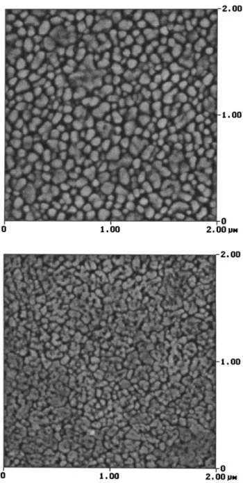
We have used AFM to study the microstructures of deposited PZT. As shown in Fig. 2a, the PZT film deposited on Pt has a grain size of 100 nm that is larger than the grain size of 65 nm for PZT deposited on Al2O3/Si shown in Fig. 2b. The reason for polycrystal-line PZT on Pt with larger grain size than on Al2O3 is because polycrystalline PZT may be more easily nucleated on polycrystalline Pt than on amorphous Al2O3. The roughness of PZT on Pt is 4.48 nm that is also larger than 1.96 nm of PZT on Al2O3/Si. The larger rms roughness of PZT on Pt is due to the larger polycrystalline grains of PZT formed on polycrystalline Pt instead of amorphous Al2O3.
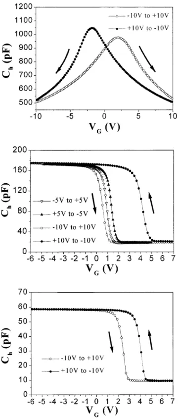
C-V characteristics at 1 MHz were further measured to study the electrical properties of PZT on Pt and Al2O3buffered Si. Figure 3a shows C-V characteristics of PZT films on Pt and the C-V curves with a typical butterfly pattern because of the ferroelectric nature of PZT.13,14Although the C-V curves are slightly asymmetric, a large peak voltage difference of 3.59 V is obtained after⫾10 V applied bias that is due to the ion shift by the electric field. This large memory window is important for memory device design rather than symmetric concern. Figure 3b shows C-V characteristics of PZT zE-mail: [email protected]
Journal of The Electrochemical Society, 148共11兲 F203-F206 共2001兲 0013-4651/2001/148共11兲/F203/4/$7.00 © The Electrochemical Society, Inc.
F203
) unless CC License in place (see abstract).
ecsdl.org/site/terms_use
address. Redistribution subject to ECS terms of use (see
140.113.38.11
films on Al2O3/Si. The hysteresis in C-V curves is due to the ferro-electric properties of PZT, which is negligible in Al2O3 gate dielectric.10,11 The small capacitance value at positive gate bias shown in Fig. 3b is due to the small series capacitance in the Si depletion region. However, there is no such effect on the MFM structure shown in Fig. 3a because of the negligible depletion width of the metal. Besides the voltage drop in Al2O3gate dielectric, the threshold voltage shift (⌬VT) measured in PZT on Al2O3/Si is 3.6 V that is almost the same as that in MFM case shown in Fig. 3a. The higher threshold voltage shift is important because it will give a large memory window. Because the threshold voltage shift is di-rectly related to the electric field in PZT (EPZT), we have therefore solved the EPZTof the stacked gate PZT/Al2O3as
EPZT⫽ Vg
冒
冉
dPZT⫹ PZT Al2O3dAl
2O3
冊
关1兴where is the dielectric constant and d the thickness of thin films. This equation is from the electric field continuity in PZT and Al2O3 by the relation
EAl2O3⫽ EPZT PZT
Al2O3 关2兴
According to Eq. 1, a smaller dielectric constant or a thinner thick-ness of PZT will increase EPZTin our stacked gate structure and hence increase the memory window. The large memory window for PZT on Al2O3/Si is due to the relative by smaller dielectric constant of 121 obtained from C-V, which is lower than that of 515 for PZT on Pt. The large dielectric constant in the MFM capacitance may be due to the larger grain size of ferroelectric films shown in Fig. 2a. We have also studied the thickness-dependent memory effect. Figure 3c shows a thicker 420 nm PZT on Al2O3/Si stacked gate dielectric. A small memory window of only 2 V is obtained for the same⫾10 V applied voltages, and the small gate capacitance of 60 pF is also not desirable for MOSFET application.
We have also investigated the capacitor leakage current because it is one of the important properties of capacitors. Figure 4a and b Figure 1. XRD patterns of 250 nm PZT on共a, top兲 Pt/Ti/SiO2/Si and共b,
bottom兲 4 nm Al2O3/Si.
Figure 2. AFM images of 250 nm PZT on共a, top兲 Pt/Ti/SiO2/Si and共b, bottom兲 4 nm Al2O3/Si.
Journal of The Electrochemical Society, 148共11兲 F203-F206 共2001兲 F204
) unless CC License in place (see abstract).
ecsdl.org/site/terms_use
address. Redistribution subject to ECS terms of use (see
140.113.38.11
show leakage current density-voltage (J-V) characteristics in MFM and MFS structures, respectively. The leakage current density of PZT on Pt is 1.0⫻ 10⫺5A/cm2at⫺10 V that is comparable to the previously reported data.15 A high breakdown electric field of 1.2⫻ 106V/cm also suggests the good PZT quality. In contrast, the leakage current density of PZT on Al2O3/Si is only 3.1⫻ 10⫺8A/cm2at⫺10 V that is nearly three orders of magnitude
lower than that in the MFM structure. Because the dielectric leakage current is the well known Fowler-Nordheim共F-N兲 tunneling at high field, the smaller leakage current is due to the additional large band-gap Al2O3gate dielectric10because of the exponential dependence of F-N tunneling current on the bandgap
J⫽ q 3E D 2 162ប DmD* exp
冉
⫺4共2mD*兲 0.5 D 3/2 3បqED冊
关3兴where ED, mD*, andD are the dielectric electric field, effective mass, and barrier height, respectively.
Table I summarizes the comparison of PZT on Pt and Al2O3/Si. The advantages of PZT on Al2O3/Si are the smaller leakage current, smoother surface, and comparable memory window with PZT on Pt. The relatively lower dielectric constant is desirable for PZT in a stacked gate dielectric because the larger electric field will drop on PZT which will in turn give a larger memory window. The success-ful integration PZT on Al2O3without an interface reaction is impor-tant for further 1T FeMOSFET development.16,17
Conclusions
We have compared PZT on Pt and 4 nm Al2O3/Si substrates. Both MFM and MFS capacitors show good capacitance-voltage characteristics and almost the same threshold voltage shift of 3.6 V. The PZT/Al2O3/Si further has nearly three orders magnitude lower leakage current density at⫺10 V than that of PZT/Pt. The compa-Figure 3. C-V curves of共a, top兲 250 nm PZT on Pt/Ti/SiO2/Si, 共b, center兲
250 nm PZT on 4 nm Al2O3/Si, and 共c, bottom兲 420 nm PZT on 4 nm
Al2O3/Si.
Figure 4. J-V curves of 250 nm PZT on 共a, top兲 Pt/Ti/SiO2/Si and 共b,
bottom兲 4 nm Al2O3/Si.
Journal of The Electrochemical Society, 148共11兲 F203-F206 共2001兲 F205
) unless CC License in place (see abstract).
ecsdl.org/site/terms_use
address. Redistribution subject to ECS terms of use (see
140.113.38.11
rable memory characteristics and the lower leakage current of PZT on Al2O3/Si are important for continuous scaling down of the ferro-electric memory.
Acknowledgments
This work has been support by the National Science Council of Taiwan, contract NSC88-2218-009-011 and NSC89-2215-E-009-100.
National Chiao Tung University assisted in meeting the publication costs of this article.
References 1. J. F. Scott, Phys. World, 8:2, 46共1995兲.
2. W. Wu, K. H. Wong, C. L. Mak, C. L. Choy, and Y. Z. Zhang, J. Appl. Phys., 88, 2068共2000兲.
3. D. Bao, N. Mizutani, X. Yi, and L. Zhang, Appl. Phys. Lett., 77, 1041共2000兲. 4. N. A. Basit, H. K. Kim, and J. Blachere, Appl. Phys. Lett., 73, 3941共1998兲. 5. Y. Chen, Y. K. Fang, M. J. Sun, and J.-R. Chen, Appl. Phys. Lett., 69, 812共1996兲.
6. S. H. Kim, D. J. Kim, J. P. Maria, A. I. Kingon, S. K. Streiffer, J. Kim, O. Auciello, and A. R. Krauss, Appl. Phys. Lett., 76, 496共2000兲.
7. S. Y. Chen and V. C. Lee, J. Appl. Phys., 87, 3050共2000兲. 8. S. Y. Chen and V. C. Lee, J. Appl. Phys., 87, 8024共2000兲.
9. Y. Shichi, S. Tanimoto, T. Goto, K. Kuroiwa, and Y. Tarui, Jpn. J. Appl. Phys., Part 1, 33, 5172共1994兲.
10. A. Chin, Y. H. Wu, S. B. Chen, C. C. Liao, and W. J. Chen, in Proceedings of Symposium on VLSI Technology, 16共2000兲.
11. A. Chin, C. C. Liao, C. H. Lu, W. J. Chen, and C. Tsai, in Proceedings of Sympo-sium on VLSI Technology, 135共1999兲.
12. J. M. Schwartz, L. F. Francis, and L. D. Schmidt, Mater. Res. Soc. Symp. Proc.,
310, 281共1993兲.
13. K. R. Udayakumar, P. J. Schuele, J. Chen, S. B. Krupanidhi, and L. E. Cross, J. Appl. Phys., 77, 3981共1995兲.
14. F. K. Chai, J. R. Brews, R. D. Schrimpf, and D. P. Birnie III, J. Appl. Phys., 82, 2505共1997兲.
15. D. Dimos, R. W. Schwartz, and S. J. Lockwood, J. Am. Ceram. Soc., 77, 3000 共1994兲.
16. A. Chin, M. Y. Yang, C. L. Sun, and S. Y. Chen, IEEE Electron Device Lett., 22 共2001兲.
17. A. Chin, M. Y. Yang, S. B. Chen, C. L. Sun, and S. Y. Chen, in Proceedings of 59th Device Research Conference, Notre Dame, IN, June 2001.
Table I. Characteristics of MFM and MFS capacitors.
⌬VT共V兲
at⫾10 V of PZT Grain size共nm兲 of PZT RMS roughness共nm兲 of PZT Leakage current density共A/cm2兲 at ⫺10 V
MFM 3.59 515 ⬃100 4.48 1.0⫾ 10⫺5
MFS 3.60 121 ⬃65 1.96 3.1⫾ 10⫺8
Journal of The Electrochemical Society, 148共11兲 F203-F206 共2001兲 F206
) unless CC License in place (see abstract).
ecsdl.org/site/terms_use
address. Redistribution subject to ECS terms of use (see
140.113.38.11