4282 Journal of The Electrochemical Society, 147 (11) 4282-4288 (2000) S0013-4651(00)01-051-X CCC: $7.00 © The Electrochemical Society, Inc.
To obtain a longer data retention time for nonvolatile memories, polyoxides with a low-leakage current, high dielectric strength, and high charge to breakdown1-3Q
bdare required. However, a rough
sur-face at the polyoxide/polysilicon intersur-face and the nonuniformity of polyoxide thickness result in a high local electric field. This high local electric field causes the polyoxide to exhibit a high leakage current and lower dielectric breakdown field in comparison with the silicon dioxide grown from a single crystalline silicon substrate.4-8It
is well known that the integrity of polysilicon oxide depends strong-ly on the oxidants used for growth or postoxidation annealing.9-15
Polyoxide has been demonstrated to have an improved electric prop-erty when it is grown in N2O ambient.14,15Such an improvement is
due to the incorporation of nitrogen by using N2O. In other words, oxide deposited by chemical vapor deposition (CVD) and annealed in N2/N2O has a relatively smooth surface at the polyoxide/poly-Si interface compared with that grown by thermal oxidation.10-13Such
a smooth surface results from the fact that the grain boundaries of the bottom polysilicon do not propagate into the polyoxide film. Another approach to improving the surface morphology of poly-Si is to use an adequately controlled chemical mechanical polishing (CMP) process for bottom polysilicon film.16,17The planar surface
morphology, after CMP, has been shown to result in an improved integrity of polyoxide.
Hence, in this paper, for the first time, the integrity of tetraethyl-orthosilicate (TEOS) polyoxide has been studied using CMP and a high temperature rapid thermal annealing (RTA) step. Polyoxides deposited by low pressure chemical vapor deposition (LPCVD) TEOS with subsequent steps using CMP and RTA show superior performance, for example, a better current-electric field (J-E) curve, higher Qbd, and lower electron trapping rate. The characteristics of TEOS polyoxide annealed in N2O at different temperatures are also discussed. Furthermore, the surface roughness and surface morphol-ogy of polyoxide/poly-Si interface are characterized using atomic face microscopy (AFM) and transmission electron microscopy (TEM) analyses. Finally, secondary-ion mass spectrometry (SIMS) analysis is performed to investigate depth profiles of nitrogen.
Experimental
In this work, n1poly-Si/ polyoxide/n1poly-Si capacitors were fabricated. Samples were fabricated on p-type silicon (100) wafers of which they were oxidized to grow 2000 Å silicon dioxide films. Subsequently, a 3000 Å poly-Si film, poly-1, was deposited at 6208C and doped by POCl3(with a sheet resistance of 50-70 V/h). The
rugged surface of the poly-Si films were polished by using the CMP process,16and the wafer was cleaned in a scrubber and ultrasonic oscillator with NH4OH:H2O2:H2O (1:1:10) solution to remove the
particles and metallic contamination. Next, an additional RCA clean process was performed to ensure the cleanness of the surface. The polyoxide film, about 114 Å, was deposited by LPCVD TEOS at 7008C on both CMP and non-CMP samples. Then, the samples were split to receive high temperature RTA for 30 s in N2(850, 9508C) or in N2O (750-10508C) ambient. After that, poly-2 was deposited and doped to have a sheet resistance of 50-70 V/h by POCl3. Poly-2 was defined and etched to form the capacitors. All samples were ther-mally oxidized to grow a 1000 Å thick oxide using a wet oxidation process. Contact holes were opened and aluminum was sputtered and patterned to form electrodes connecting poly-2.
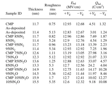
Table I lists all of the device types fabricated in this work along with their measurement data for breakdown field (Ebd) and Qbd, per-formed under constant current stress of 110 mA for 1Vginjection
and at 210 mA for 2Vg injection. The area of capacitors is 6 3
1024cm2. The thickness of polysilicon oxide was measured by using
the Keithley capacitance-voltage method. The surface roughness in root mean square (rms) was studied using AFM. To reveal the actu-al surfaces of our samples, the surface morphology was measured after the stripping of the TEOS polyoxide in diluted HF solution. Electrical characteristics and constant current stress were measured using an HP4145 semiconductor parameter analyzer. The surface morphology of the polyoxide was also studied by TEM. Finally, the depth profiles of nitrogen were investigated using SIMS.
Characteristics of TEOS Polysilicon Oxides: Improvement by CMP and
High Temperature RTA N
2
/N
2
O Annealing
Jiann Heng Chen,
aTan Fu Lei,
a,zJian-Hong Chen,
aand Tien Sheng Chao
baDepartment of Electronics Engineering and Institute of Electronics, National Chiao Tung University, Hsinchu, Taiwan bNational Nano Device Laboratory, Hsinchu, Taiwan
The integrity of tetraethylorthosilicate (TEOS) polyoxide using chemical mechanical polishing (CMP) plus a high temperature rapid thermal annealing (RTA) step was studied in this work. The surface morphology of polysilicon is improved after a CMP process. Polyoxides deposited by low pressure chemical vapor deposition (LPCVD) TEOS in conjunction with CMP and RTA N2/N2O annealing exhibit a better current-electric field (J-E) curve, higher charge to breakdown ratio, and lower electron trapping rate. In addition, the composite bilayer (TEOS deposited and thermally grown by RTA) polyoxide film introduces an asymmetry of electrical leakage current, trapping characterization, and charge to breakdown, with respect to the injection of different polarity (1Vgand 2Vg).
© 2000 The Electrochemical Society. S0013-4651(00)01-051-X. All rights reserved. Manuscript submitted January 16, 2000; revised manuscript received July 21, 2000.
Table I. List of the device types fabricated.
Roughness Ebd Qbd Thickness rms (MV/cm) (C/cm 2) Sample ID (nm) (nm) 1Vg 2Vg 1Vg 2Vg CMP 11.7 0.75 12.93 12.68 4.51 1.32 As-deposited As-deposited 11.4 5.13 12.83 12.67 13.01 11.24 CMP 850N2 11.7 0.82 12.96 12.86 17.69 11.87 850N2 11.4 5.24 12.91 12.76 14.54 11.29 CMP 950N2 11.7 0.96 13.23 13.18 13.39 12.23 950N2 11.4 5.34 12.93 12.92 17.25 11.96 CMP 750N2O 12.6 1.11 13.19 13.05 27.98 13.16 750N2O 12.3 5.12 12.92 12.92 21.07 12.33 CMP 850N2O 13.6 1.25 12.88 12.63 33.07 14.57 850N2O 13.3 5.31 12.71 12.56 24.21 14.04 CMP 950N2O 14.9 1.51 12.75 11.63 14.17 10.28 950N2O 14.5 5.36 12.62 11.44 11.97 18.46 CMP 1050N2O 15.9 1.71 12.71 12.41 10.02 12.27 1050N2O 15.5 5.35 12.61 12.32 9.18 10.08
Results and Discussion
Table I lists various samples fabricated in this work along with their measurement data for surface rms, Ebd, and Qbd, performed under 110 mA for 1 Vginjection and 210 mA for 2Vginjection.
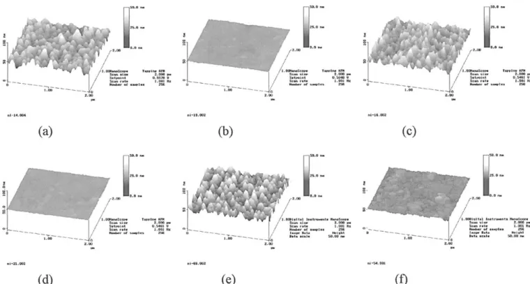
Figures 1a-f depict the surface morphology images of polyox-ide/poly-Si interfaces for samples investigated by AFM. To disclose the actual surface of the poly-Si layers after the deposition, dilute HF solution was used to strip the oxides. Figures 1a-b illustrate the orig-inal surface of non-CMP and CMP samples after the deposition of TEOS polyoxide. With the information provided by these two fig-ures we find that the surface morphology can be improved signifi-cantly by using CMP. Figures 1c and e display the AFM image of the non-CMP poly-Si after annealing samples in N2or N2O ambient, respectively. A rough and nonuniform surface was observed. CMP processed samples, after annealing in either N2 or N2O ambient, exhibited a smooth and uniform surface, as shown in Fig. 1d and f. As for the non-CMP samples, the initial surface roughness (5.1-5.2 nm) found in Fig. 1a of the polyoxide/poly-Si interface was almost the same as those after RTA annealing processed in N2or N2O ambient (5.2-5.4 nm) as presented in Fig. 1c and e. As for the CMP samples, the initial surface roughness (0.7-0.8 nm) observed in Fig. 1b was only slightly increased as compared with those after RTA annealing both in N2 (0.8-1.0 nm) or in N2O ambient (1.2-1.5 nm), as shown in Fig. 1d-f, respectively.
Figures 2a and b present the cross section of TEM for non-CMP and CMP samples, while Fig. 2c and d show the corresponding sam-ples which were annealed in N2O ambient. As can be seen from these figures, the CMP samples in Fig. 2b and d have smoother sur-faces than those of the non-CMP samples shown in Fig. 2a and c.
Figures 3a and b depict the SIMS depth profiles of nitrogen for the samples manufactured in this experiment. The actual percentage of N2was normalized with respect to the counts of Si in the sample. As shown in Fig. 3a, a significant amount of nitrogen existed at the TEOS polyoxide/poly-1 interface for the N2O annealed sample despite the fact that a much smaller amount was found for the N2 annealed sample and the control one. The nitrogen incorporated at the TEOS polyoxide/poly-1 interface has been reported to have the
effects of improving TEOS quality.12,13Figure 3b indicates that the
nitrogen profile of the CMP sample after RTA annealing in N2O ambient exhibits the narrowest and largest peak distribution among all of the samples. It is evident that during the high temperature ther-mal oxidation the oxidant might diffuse into deeper distance through the grain boundary via the rough (or nonuniform) surface and create a broader and deeper N2distribution, similar to the conclusion de-rived from previous investigation.17
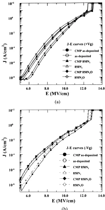
Figures 4a and b present the J-E characteristics of polyoxides. The J-E curve is calculated by using the initial current-voltage (I-V) curve of the polyoxide, where J = I/(area of capacitors) and E =
Figure 1. Surface image measured by AFM for (a) non-CMP as-deposited, (b) CMP as-deposited, (c) non-CMP sample after 8508C N2RTA annealing, (d) CMP
sample after 8508C N2RTA annealing, (e) non-CMP sample after 8508C N2O RTA annealing, (f) CMP sample after 8508C N2O RTA annealing.
Figure 2. The TEM micrographs of (a) non-CMP deposited, (b) CMP as-deposited, (c) non-CMP sample after 8508C N2O RTA annealing, (d) CMP
4284 Journal of The Electrochemical Society, 147 (11) 4282-4288 (2000) S0013-4651(00)01-051-X CCC: $7.00 © The Electrochemical Society, Inc. V/(thickness of oxide). Obviously, for both N2 and N2O annealed
polyoxides, CMP samples resulted in a lower leakage current than those of non-CMP samples under both positive (1Vg) poly-1 and
negative (2Vg) poly-2 injection. This phenomenon is attributed to
the high local electric field caused by the nonuniformity of thickness in the polyoxide film and the asperity at the polyoxide/poly-1 inter-face,1especially for the non-CMP samples.16 In other words, the smooth surface of polyoxide/poly-1 of the CMP sample contributes to a smaller localized current density; therefore, under the same elec-trical field, an improved uniformity of localized electric field is obtained for CMP samples as compared with non-CMP samples.
The charge trapping characteristics of the polyoxide were also investigated. Figures 5a and b show the gate voltage shifts of sam-ples under 110 mA (1Vg) and 210 mA (2Vg) constant current
stress. It is noted that the voltage shift is reduced after high temper-ature RTA N2/N2O annealing. Furthermore, all of the CMP samples had smaller voltage shifts than those of non-CMP samples under either 1Vgor 2Vg stress based on these figures. This phenomenon
suggests that CMP samples would trap fewer electrons than those of non-CMP samples. On the other hand, it is also expected that a rugged polyoxide/poly-Si interface (non-CMP) can easily generate certain localized trapping sites to induce local current, thus causing a higher electron trapping.
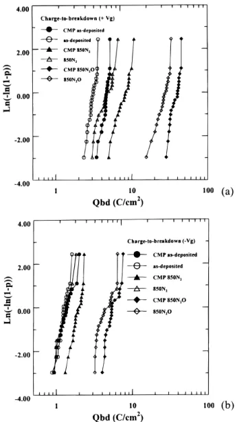
Figures 6a and b illustrate the Qbdcharacteristics of these sam-ples under 110 mA (1Vg) and 210 mA (2Vg) gate injections. It is
worth mentioning that the Qbdof the TEOS polyoxide is increased after annealing at high temperature RTA using N2/N2O. Also, the CMP sample demonstrates a larger Qbdthan that of the non-CMP sample. It can be inferred that the roughness existing at a polyox-ide/poly-Si interface would provide various trap sites and lead to a higher current density with higher electron-trapping rate, capable of causing smaller Qbd values. Furthermore, it should be noted that polyoxide annealed in N2O ambient has better J-E curves, smaller voltage shifts, and larger Qbdvalues as compared with the rest of samples. The mechanism of effecting these improvements is due to the incorporation of N2 at the TEOS polyoxide/polysilicon
inter-Figure 3. SIMS depth profiles of nitrogen in (a) CMP samples, (b) non-CMP and non-CMP samples after 8508C N2/N2O RTA annealing.
Figure 4. The J-E characteristics of TEOS polyoxides under (a) 1Vg
face,12-15as shown in Fig. 3a. In respect to CVD deposition of
poly-oxide, there are two factors which will affect its electrical character-istics. One of them is the surface roughness and the other is the intrinsic trapping in the CVD oxide. We believe that the quality of a TEOS oxide would be affected more by the intrinsic effects than by the surface roughness due to the fact that the thickness of TEOS deposited was about 11 nm thick in this experiment. After high tem-perature RTA, the trap located in TEOS oxide is reduced with its dependence on surface roughness being observed, as demonstrated by CMP850N2 and 850N2 samples in Fig. 6a, b. Moreover, RTA N2 annealing with a temperature higher than 9008C can improve the quality of TEOS as shown in Table I, and this is consistent with Ref. 12.
From the results mentioned above, it is reasonable to suggest that adding an adequately controlled CMP process not only reduces the surface roughness of the poly-1 but also improves the inclusion of nitrogen during high temperature N2O annealing. Although the in-corporation of nitrogen at interface can improve the quality of poly-oxide, the rough interface degrades the performance of non-CMP samples under both 1Vg and 2Vg gate injection. By adding the
CMP process, bumps on the poly-1 surface1 are removed and a
smooth surface can be obtained. Moreover, the electrical properties of TEOS polyoxide can be improved after high temperature N2/N2O annealing. Consequently, a sequence combining high temperature
N2/N2O annealing step and CMP process should result in an opti-mized approach to processing the TEOS polyoxide.
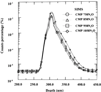
Figure 7 depicts the SIMS depth profiles of nitrogen of CMP samples after different N2O annealing temperatures in this experi-ment. As shown in this figure, the amount of nitrogen is increased as the temperature of annealing is increased.
Figures 8 shows the thickness of polyoxide and the roughness of CMP samples after high temperature N2O annealing. It is clear that the thickness of TEOS polyoxide increases as the N2O annealing tem-perature increases. Besides, the surface of TEOS polyoxide/ poly-1 interface becomes much rougher at higher temperature N2O an-nealing. At a high temperature N2O annealing process, a thin thermal polyoxide will be grown between the TEOS polyoxide and poly-1 interface, hence, the total thickness of polyoxide will be increased. During the thermal oxidation of poly-Si, grain boundaries were oxi-dized more rapidly than the central part of the grains. V-grooves at the polyoxide/poly-Si interface are formed as a result of having different oxidation rates between grain boundaries and their associated grains.5
At the same time, longer oxidation also increases the size of the grooves, the surface roughness at the polyoxide/poly-Si interface, and the nonuniformity of polyoxide film thickness.1,5,14
Figures 9a and b illustrate the J-E characteristics of TEOS poly-oxides under 1Vginjection and under 2Vginjection. It is found that,
for 1Vginjection, the leakage current of TEOS polyoxide is reduced Figure 5. The charge trapping characteristics of TEOS polyoxides under (a)
110 mA/cm2, (b) 210 mA/cm2constant current injection. Figure 6. The Qbd characteristics of TEOS polyoxides under (a)
4286 Journal of The Electrochemical Society, 147 (11) 4282-4288 (2000) S0013-4651(00)01-051-X CCC: $7.00 © The Electrochemical Society, Inc.
but the reverse trend was found under 2Vginjection. However, the
surface of the TEOS polyoxide/poly-1 becomes more rugged as the temperature of N2O annealing is increased as shown in Fig. 8. As a result, the local electrical field is increased as well due to the incre-ment of surface roughness and nonuniformity with respect to the polyoxide film.1 Again, it can be seen that the breakdown field
becomes worse for both 1Vginjection and 2Vginjection as the
tem-perature of N2O annealing is increased. Besides, the growth of a thin layer of thermal polyoxide at the TEOS polyoxide/poly-1 interface was found by using N2O annealing at high temperature. This two-layer (TEOS deposited and thermally grown) polyoxide film may introduce an asymmetry3on the electrical leakage current for
differ-ent polarity (1Vgand 2Vg) injection. Furthermore, the amount of
nitrogen at the TEOS polyoxide/poly-1 interface is increased as the annealed temperature is raised, with which it may affect the asym-metry as well.
Figures 10a and b show the shifts of gate voltage for samples under constant current stress at 110 mA (1Vg) and 210 mA (2Vg)
after annealing at different temperatures. For the 1Vg injection,
samples annealed by RTA at lower temperature (750-8508C) have a smaller voltage shift than those annealed at higher temperature (950-10508C). We attribute this result to the rugged interface between polyoxide/poly-1 that, apparently, forms a larger conducting area and a higher local current density, therefore inducing a higher trap-ping of electrons. In contrast, this is quite different for samples under 2Vginjection. It can be seen that the voltage shift is decreased as the
temperature of RTA N2O annealing is increased. This discrepancy may be attributed to the two-layer polyoxide film and/or the incor-poration of nitrogen in the TEOS polyoxide. In this work, the thick-ness of N2O-induced thermal polyoxide was around 1-4 nm. Under 1Vginjections, the electrons are injected into the polyoxide from the
polyoxide/poly-1 interface. The leakage current is reduced because of high quality N2O thermal polyoxides after high temperature N2O annealing. As temperature increases, the thickness of the N2O poly-oxide increases. But the increment of surface roughness also reduces the electron breakdown field and increases the electron trapping rate. Under 2Vginjection, the TEOS polyoxide near the
poly-2/polyox-Figure 7. SIMS depth profiles of nitrogen in CMP samples after different high temperature N2O RTA annealing.
Figure 8. Thickness and roughness of CMP samples after different high tem-perature N2O annealing.
Figure 9. The J-E characteristics of TEOS polyoxides after different high temperature N2O RTA annealing under (a) 1Vginjection, (b) 2Vginjection.
ide interface has a stronger effect than does the N2O thermal
poly-oxide near the polypoly-oxide/poly-1 interface in terms of influencing the electrical characteristics of the sample wafers. As the temperature of N2O annealing is increased, the trapping rate of TEOS polyoxide
reduces. This arises from the reduced growth of TEOS because of the competition with the growth of N2O polyoxide, which makes the
surface roughness of TEOS oxide the dominating factor for sample’s electrical characteristics. So, the leakage current increases and the breakdown field reduces after high temperature annealing.
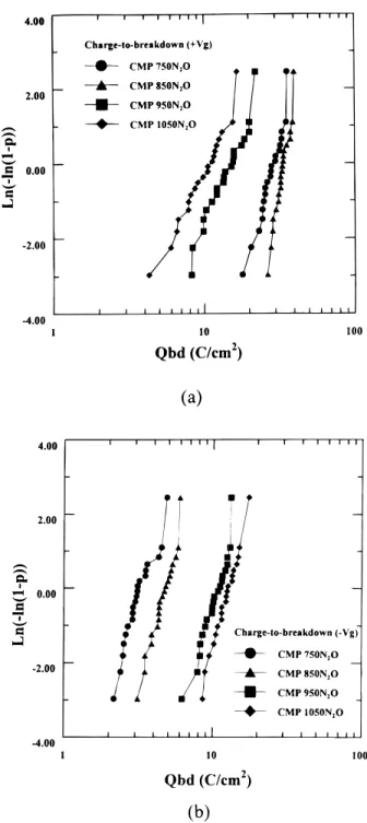
Figures 11a and b illustrate the Qbdcharacteristics of these
sam-ples under 110 mA (1Vg) and under 210 mA (2Vg) gate injection.
For the 1Vginjection, samples annealed at lower temperature
(750-8508C) RTA have greater Qbdthan those annealed at higher
temper-ature RTA (950-10508C). It is, therefore, possible that a rougher polyoxide/polysilicon interface leads to a higher local current densi-ty plus a higher electron-trapping rate, subsequently causing smaller
Qbdvalues. Moreover, at a lower temperature annealing condition,
750-8508C, Qbdcan be increased further after another cycle of high
temperature RTA annealing, but the reverse trend is found at the
higher temperature annealing condition, 950-10508C. This is quite different for samples under 2Vginjection. It can be seen that Qbdis
improved as the temperature of RTA N2O annealing is increased. The largest Qbdof polyoxide is obtained by 8508C RTA N2O anneal-ing for 1Vg injection and 10508C RTA N2O annealing for 2Vg
injection. This matches with the trapping characteristics shown in Fig. 10a and b.
Conclusions
An adequately controlled CMP process not only improves the surface roughness of poly-1 but also improves the incorporation of nitrogen during the process of N2O annealing at high temperature. The electrical characteristics of TEOS polyoxide are improved after high temperature N2/N2O annealing. Experimentally, the combina-tion of high temperature N2/N2O annealing step and CMP results in
Figure 10. The charge trapping characteristics of TEOS polyoxides after dif-ferent high temperature N2O RTA annealing under (a) 110 mA/cm2, (b)
210 mA/cm2constant current injection.
Figure 11. The Qbdcharacteristics of TEOS polyoxides after different high
temperature N2O RTA annealing under (a) 110 mA/cm2, (b) 210 mA/cm2
4288 Journal of The Electrochemical Society, 147 (11) 4282-4288 (2000) S0013-4651(00)01-051-X CCC: $7.00 © The Electrochemical Society, Inc. an optimized process for TEOS polyoxide. In this work, we find that
the increment of annealing temperature can cause the surface between TEOS polyoxide and poly-1 to become more rugged and the total thickness of polyoxide to grow thicker due to the increase of growth rate of polyoxide. Concurrently, the incorporation of N2is increased with increasing RTA temperature. As the result, this bilay-er (TEOS deposited and thbilay-ermally grown by RTA) polyoxide film may introduce an asymmetry of electrical leakage current, trapping characterization, and Qbdfor different polarity (1Vgand 2Vg) injec-tion. Consequently, the optimized high temperature annealing process for TEOS polyoxide is acquired at 8508C using RTA N2O annealing for 1Vginjection and at 10508C using RTA N2O anneal-ing for 2Vginjection.
Acknowledgment
This paper was supported by the National Science Council of Taiwan, Republic of China, under contract no. NSC8P-2215-E00P-306.
National Chiao Tung University assisted in meeting the publication costs of this article.
References
1. J. C. Lee and C. Hu, IEEE Trans. Electron Devices, 35, 1063 (1988).
2. L. Faraone, R. D. Vibronek, and J. T. Mcginn, IEEE Trans. Electron Devices, 32, 577 (1985).
3. S. L. Wu, C. Y. Chen, T. Y. Lin, C. L. Lee, T. F. Lei, and M. S. Liang, IEEE Trans. Electron Devices, 44, 153 (1997).
4. M. Hendriks, and C. Mavero, J. Electrochem. Soc., 138, 1466 (1991). 5. M. C. Jun, Y. S. Kim, and M. K. Han, Appl. Phys. Lett., 66, 2206 (1995). 6. P. A. Heimann, S. P. Murarka, and T. T. Sheng, J. Appl. Phys., 53, 6241 (1982). 7. L. Faraone and G. Harbeke, J. Electrochem. Soc., 133, 1410 (1986).
8. E. Avni, O. Abramson, Y. Sonnenblick, and J. Shappir, J. Electrochem. Soc., 135, 182 (1988).
9. F. C. Jong, T. Y. Huang, T. S. Cho, H. C. Lin, L. Y. Leu, K. Young, C. H. Lin, and K. Y. Chiu, IEEE Electron Device Lett., 18, 343 (1997).
10. P. Candelier, F. Mondon, B. Guillaumot, G. Reimbold, and F. Martin, IEEE Elec-tron Devices Lett., 16, 385 (1995).
11. J. Kim and S. T. Ahn, IEEE Electron Device Lett., 18, 385 (1997).
12. C. H. Kao, C. S. Lai, and C. L. Lee, IEEE Trans. Electron Devices, 44, 526 (1997). 13. C. H. Kao, C. S. Lai, and C. L. Lee, IEEE Trans. Electron Devices, 45, 526 (1998). 14. C. S. Lai, T. F. Lei, and C. L. Lee, IEEE Trans. Electron Devices, 43, 326 (1996). 15. Z. Liu, H. J. Wann, P. K. Ko, C. Hu, and Y. C. Cheng, IEEE Electron Device Lett.,
13, 402 (1997).
16. T. F. Lei, J. Y. Cheng, S. Y. Shiau, T. S. Chao, and C. S. Lai, IEEE Trans. Electron Devices, 45, 912 (1998).
17. T. F. Lei, J. H. Chen, M. F. Wang, and T. S. Chao, IEEE Electron Device Lett., 20, 235 (1999).