Efficiency droop behaviors of InGaN / GaN multiple-quantum-well
light-emitting diodes with varying quantum well thickness
Y.-L. Li,a兲Y.-R. Huang, and Y.-H. Lai
Institute of Photonics and Optoelectronics, National Taiwan University, Taiwan 10617, Republic of China
共Received 13 September 2007; accepted 12 October 2007; published online 31 October 2007兲 InGaN / GaN multiple-quantum-well共MQW兲 light-emitting diodes with varied InGaN quantum well thicknesses are fabricated and characterized. The investigation of luminous efficiency versus current density reveals a variety of efficiency droop behaviors. It is found that the efficiency droop can be drastically reduced by increasing the quantum well thickness of the MQW structures. On the other hand, relative internal quantum efficiency共IQE兲 measurements indicate that a thinner well results to higher IQEs owing to the greater spatial overlap of electron and hole distribution functions. © 2007 American Institute of Physics. 关DOI:10.1063/1.2805197兴
InGaN / GaN based high-brightness light-emitting diodes 共LEDs兲 have attracted much attention because of their appli-cations in signage, back lighting, and general illumination. Many efforts have been made to improve material quality,1,2 light extraction efficiency,3and metal-semiconductor Ohmic contacts.4 In addition, emission efficiencies of InGaN / GaN LEDs have been improved drastically during the last few years. As LED technology becomes more and more mature, it is highly desirable for LEDs to emit a high luminous flux at high current densities. However, for InGaN / GaN multiple-quantum-well共MQW兲 LEDs, a well-known funda-mental problem needs to be overcome, namely, the efficiency “droop,” which is the reduction in efficiency as the current is increased.5,6The strong efficiency droop is not observed for other material systems, such as AlGaInP–GaAs, and it is not very clear what mechanism causes the droop in InGaN / GaN material system.
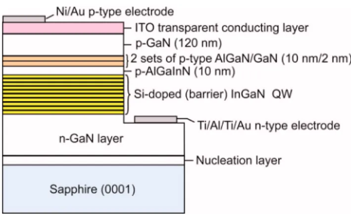
In this letter, InGaN / GaN-based blue LEDs with various quantum well thicknesses are investigated. Electrical and op-tical characteristics of the LEDs are presented and discussed. The InGaN / GaN MQW LED samples used in this study are grown on a c-plane共0001兲 sapphire substrate with a Veeco metal-organic chemical vapor deposition system using a high speed rotating disk with a vertical gas-flow growth chamber. Trimethylgallium 共TMGa兲, trimethylindium 共TMIn兲, trim-ethylaluminum 共TMAl兲, and ammonia 共NH3兲 are used as
source materials of Ga, In, Al, and N, respectively. Bi-cyclopentadienyl magnesium共Cp2Mg兲 and silane 共SiH4兲 are used as the p-type and n-type doping precursors, respec-tively. On top of the sapphire substrate, a 20 nm thick GaN nucleation layer is grown at low temperature followed by a thick共4m兲 n-type GaN buffer layer.
After buffer layer growth, a ten-period InGaN / GaN MQW active region on top of the buffer layer is grown. Triethylgallium共TEGa兲 is used as the Ga source material for the MQW growth. The growth rates for both barriers and wells are controlled at about 1.5 nm/ min. Note that all bar-riers are doped with Si whereas the wells are left undoped. A thin共10 nm兲 Mg doped p-type AlGaInN is grown on top of MQW and followed by two sets of p-type AlGaN / GaN 共10 nm/2 nm兲 layers which serve as electron-blocking layer. Finally, a Mg doped p-type GaN cladding layer共120 nm兲 is
grown where the top region of the cladding layer is heavily Mg doped to facilitate Ohmic contact formation. For pro-cessing, LED chips 共350⫻350m2兲 utilizing transparent
conducting indium tin oxide layers are fabricated using a standard LED process.7Ni/ Au and Ti/ Al/ Ti/ Au metalliza-tions are deposited by e-beam evaporation to serve as p-type and n-type Ohmic contacts, respectively. The schematic structure of the processed LED samples is shown in Fig.1.
This study has the purpose to understand the relationship between the efficiency droop and the thickness of the quan-tum wells. The barrier thickness of the MQWs is fixed at 12 nm while the thickness of the well is varied by changing the growth time. The growth times of each well in these samples are 1 min 共1.5 nm兲, 0.8 min 共1.2 nm兲, 0.6 min 共0.9 nm兲, and 0.4 min 共0.6 nm兲, respectively.
As-grown wafers are characterized by measuring photo-luminescence as a function of temperature. The experiments are performed using a 10– 300 K variable-temperature cry-ostat. The samples are optically pumped with a 50 mW He–Cd laser emitting at 325 nm. After chip fabrication, LEDs are characterized with a wafer prober. dc and pulsed currents are injected by a Keithley 2400 source meter. Elec-troluminescence共EL兲 spectrum and intensities are measured by a high-resolution spectrometer with an optical fiber col-lecting the light emitted from the top of the LED.
The temperature-varied photoluminescence 共PL兲 mea-surement, shown in Fig. 2, gives the relative internal quantum efficiencies共IQEs兲 for these samples at room
tem-a兲Electronic mail: [email protected] FIG. 1.well LEDs with varied well thicknesses.共Color online兲 Schematic structure InGaN/GaN
multiple-quantum-APPLIED PHYSICS LETTERS 91, 181113共2007兲
0003-6951/2007/91共18兲/181113/3/$23.00 91, 181113-1 © 2007 American Institute of Physics
perature. It is known that the carrier recombination is domi-nated by nonradiative recombination at a room temperature in the InGaN / GaN system, whereas at low temperatures, it is dominated by radiative recombination. The relative IQE is estimated by comparing the low temperature共10 K兲 with the RT-PL共300 K兲 assuming that the PL internal quantum effi-ciency at low temperature共10 K兲 is equal to 1. The inspec-tion of Fig.2reveals that the thicker the wells are, the lower the relative IQE at room temperatures. This is attributed to the larger electron-hole charge separation induced by internal field with thicker wells.8,9
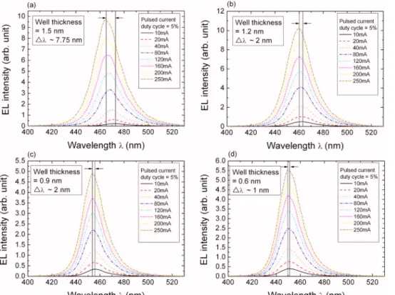
Room-temperature EL spectra under different pulsed in-jection currents are shown in Fig. 3. The pulsed currents have a 5% duty cycle and the pulsed injection duration is 3 ms. Figure3shows that the peak of the emission spectrum shifts toward shorter wavelengths共blueshift兲 with increasing injection currents. It is also shown in the figure that less blueshift is observed for MQWs with thinner wells. This can be explained by Coulomb screening of the piezoelectric-field-induced quantum confined Stark effect共QCSE兲, that is, the internal polarization field is compensated by injecting carriers. The blueshift phenomenon is due to the compensa-FIG. 2. 共Color online兲 Temperature-varied共from 10 to 300 K兲 photolumi-nescence measurements for room-temperature IQE assessment of InGaN / GaN MQW LEDs with varied well thicknesses.
FIG. 3. 共Color online兲 Room-temperature EL spectra of MQW LEDs with varied well thicknesses un-der various injection currents. The peaks of the emission spectra shift to-ward shorter wavelengths 共blueshift兲 as the current is increased from 10 to 250 mA, as indicated by the two vertical lines.
181113-2 Li, Huang, and Lai Appl. Phys. Lett. 91, 181113共2007兲
tion of internal polarization field. A thinner quantum well structure results in less QCSE-induced wavelength shift so that the magnitude of blueshift is less.10 At the same time, the radiative recombination rate is raised because the reduc-tion of the internal field enhances the spatial overlap of elec-trons and holes that are otherwise separated by the strong internal field within the MQWs.
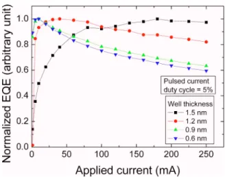
Figure 4 shows the normalized external quantum effi-ciency curves with varied thicknesses of wells under differ-ent currdiffer-ent densities. To prevdiffer-ent heating, LEDs are operated under pulsed current injection. Investigating Fig. 4 reveals that MQW structures with thick wells could drastically re-duce the efficiency droop effect. For samples with well widths of 1.2, 0.9, and 0.6 nm, efficiency peaks can be ob-served at 25, 7, and 7 mA, respectively. Very little efficiency droop is observed for the LED with the thickest 共1.5 nm兲 well design. In this case, the efficiency drop from the highest value at low current density to 200 A / cm2 is less than 3%.
We propose that the strong droop effect for InGaN / GaN MQW LEDs is mainly due to the carrier overflow under high applied current densities, consistent with Refs. 11 and 12, instead of thermal heating. LEDs with thicker wells lead to less carrier overflow and thus reduce droop effect. However, since the internal polarization field is too strong to be com-pensated even under 200 A / cm2,13the thicker well structure results to a larger spatial separation of electrons and holes
and thus reduces the radiative recombination rate, as shown in Fig.2.
According to the previous discussion, there seems to be a trade-off to achieve both high efficiency and “no droop” for InGaN / GaN LEDs grown along c-plane direction. Heavily doping the barriers with Si may help resolve the issue but at the same time, could reduce the material quality and thus enhance nonradiative recombination. The other possibility is to reduce the internal polarization field by material growth along nonpolar direction.
In conclusion, InGaN / GaN-based MQW LEDs with various well thicknesses have been fabricated and character-ized. We have demonstrated that the droop effect can be drastically reduced to less than 5% at a current density as high as 200 A / cm2. Relative IQE measurements show that thicker well structures lead to a lower radiative recombina-tion rate caused by the larger spatial separarecombina-tion of electrons and holes, which in turn is caused by the strong internal polarization field.
Support by Taiwan National Science Council and For-mosa Epitaxy, Inc. is gratefully acknowledged. The authors would like to thank Professor E. F. Schubert and Dr. R. F. Karlicek for fruitful discussions.
1S. Nakamura, M. Senoh, N. Iwasa, and S. Nagahama, Jpn. J. Appl. Phys., Part 2 34, L797共1995兲.
2T. Mukai, S. Nagahama, M. Sano, T. Yanamoto, D. Morita, T. Mitani, Y. Narukawa, S. Yamamoto, I. Niki, M. Yamada, S. Sonobe, S. Shioji, K. Deguchi, T. Naitou, H. Tamaki, Y. Murazaki, and M. Kameshima, Phys. Status Solidi A 200, 52共2003兲.
3J. K. Kim, T. Gessmann, E. F. Schubert, J.-Q. Xi, H. Luo, J. Cho, C. Sone, and Y. Park, Appl. Phys. Lett. 88, 013501共2006兲.
4Y.-L. Li, E. F. Schubert, and J. W. Graff, Appl. Phys. Lett. 76, 2728 共2000兲.
5T. Mukai, M. Yamada, and S. Nakamura, Jpn. J. Appl. Phys., Part 1 38, 3976共1999兲.
6M. R. Krames, O. B. Shchekin, R. Mueller-Mach, G. O. Mueller, L. Zhou, G. Harbers, and M. G. Craford, J. Disp. Technol. 3, 160共2007兲. 7Y. C. Lin, S. J. Chang, Y. K. Su, T. Y. Tsai, C. S. Chang, S. C. Shei, C. W.
Kuo, and S. C. Chen, Solid-State Electron. 47, 849共2003兲. 8J. Bai, T. Wang, and S. Sakai, J. Appl. Phys. 88, 4729共2000兲.
9T. Wang, D. Nakagawa, M. Lachab, T. Sugahara, and S. Sakai, Appl. Phys. Lett. 74, 3128共1999兲.
10A. Hangleiter, J. S. Im, H. Kollmer, S. Heppel, J. Off, and F. Scholz, MRS Internet J. Nitride Semicond. Res. 3, 15共1998兲.
11M. C. Schmidt, K.-C. Kim, H. Sato, N. Fellows, H. Masui, S. Nakamura, S. P. Denbaars, and J. S. Speck, Jpn. J. Appl. Phys., Part 2 46, L126 共2007兲.
12K.-C. Kim, M. C. Schmidt, H. Sato, F. Wu, N. Fellows, M. Saito, K. Fujito, J. S. Speck, S. Nakamura, and S. P. Denbaars, Phys. Status Solidi 共RRL兲: Rapid Res. Lett. 1, 125 共2007兲.
13G. Franssen, T. Suski, P. Perlin, R. Bohdan, A. Bercha, W. Trzeciakowski, I. Makarowa, P. Prystawko, M. Leszczyński, I. Grzegory, S. Porowski, and S. Kokenyesi, Appl. Phys. Lett. 87, 041109共2005兲.
FIG. 4. 共Color online兲 Normalized external quantum efficiency measure-ments of the MQW LEDs with varied well thicknesses. Measuremeasure-ments are pulsed with 5% duty cycle. For samples with different well thicknesses, the efficiency drop from the highest value at low current density to 200 A / cm2 is 2.7%, 17.9%, 36.7%, and 40.4%, respectively. This figure clearly illus-trates a reduced efficiency-droop effect for thicker quantum wells.
181113-3 Li, Huang, and Lai Appl. Phys. Lett. 91, 181113共2007兲