TU4B-4
A
Broadband
HBT
MMIC IQ Modulator and
Millimeter-wave Vector Signal Characterization
Hong-Yeh Chang*, Tian-Wei €hang*, Huei Wang*,
Yu-Chi Wang**, Pane-Chane Chao** and Chung-Hsu Chen**
*
Department
of Electrical Engineering and Graduate Institute
of
Communication Engineering,
National Taiwan University, Taipei, Taiwan
106,
ROC
**
WIN Semiconductors Corp., Hwaya Technology Park, Taoyuan, Taiwan 333, ROC
AbsfracI - A broadband 50-110 GHz HBT M M I C IQmodulator and a vector signal measurement system for millimeter-wave applications are reported in this paper. For
the digital modulation measurement, a QPSK modulation format was used with a 2-Mhps data rate for the IQ modulation. Using the 50-110 GHz vector signal measurement system, this M M I C chip shows an error vector magnitude (EVM) o f within 12 % rms and a carrier rejection of more than 21 dB. The 110-GHz operation frequency of this M M I C i s the highest among all the reported HBT vector modulators. Also, this is the first time the E V M test was performed for an IQ modulator at V-hand and W-hand. This M m C is suitable for software defined radio (SDR), linearization techniques of power amplifier and related transmitter applications both in V-band and W-hand.
1. INTRODUCTION
Direct carrier modulator has the advantages of reducing the complexity of transmitters and thus their cost. For conventional designs, the IQ modulators consist of two BPSK modulators, a 90" phase shifter and an in-phase
power combiner. Most of BPSK modulators are
composed with a doubly-balanced mixer [I]-[3] due to superior spur performance, linearity and port to port
isolation. However, they usually need a high LO drive
power and require a built-in driver amplifier. Altemately,
hy using Si (CMOS, BIT 01 SiGe HBT) and GaAs (HBT
or HEMT) technologies, the IQ modulators based on the Gilbert cell architechue have been reported in recent years
[4]-[6]. Although they showed the performance of good
amplitude and phase match and high LO rejection, most of
them operated below IO GHz.
In this paper, the IQ modulator is based on the
quadrature modulation architecture, which contains two
sets of BPSK modulators, a 90" hybrid and a combiner.
We use a balanced reflection-type phase shifter [7] for the
BPSK modulator, which utilized a Lange coupler as a 90"
hybrid and two shunt cold-mode devices as switching devices. The cold-mode devices can be fabricated with HEMT, FET, or HBT technologies. Although the BPSK
modulators can be implemented in HEMT process [7]-[9],
0-7803-7695-1/03/$17.00 0 2003 E E E
99
2003 IEEE M l 7 - S Digest
however, they require negative biasing voltage tu perform modulation function. On the Other hand, the HBT based BPSK modulators have been reported in literatures [lo]-
[I I] with operating frequency below 50 GHz. Recently,
we have reported a HBT based BPSK modulator above 50
GHz successhlly [ 121. Using this BPSK modulator in our
IQ modulator design, this MMIC chip demonstrated a superior broadband performance, good amplitudelphase match and low insertion loss.
Vector signal measurements at 38 GHz can be found in
literatures [3], [13]. For a real digital modulation signal
coming from an IQ modulator, the amplitude and phase states are time variant. The amplitude and phase states of the dynamic signal cannot be measured via a network
analyzer or a scalar spectrum analyzer. Therefore, a
vector signal analyzer was used to detect the performance of the IQ modulator such as EVM, phase error, amplitude error, quadrature error, I-Q imbalance, DC offset and the
impairment of an imperfect LO source. In this paper, we
use a QPSK modulation format with a 2-Mbps data rate to test this IQ modutator MMIC between 50 GHz and 1 IO
GHz. Due to the equipment limitations, the test is
performed only with a data rate of 2-Mbps.
11. MMIC PROCESS AND CIRCUITDESIGN
The IQ modulator design is based on the
6"
1-w GaAsHBT MMIC process on a 4-mil substrate provided by WIN Semiconductors. There are three metal layers, metal-insulator-metal (MIM) capacitors, via-holes, spiral
inductors and thin film resistors in this process. The
polyimide and SIN, are used for the isolated layer between metal and metal layers. The one emitter finger and emitter
size of 1 . 4 ~ 1 0 p2 HBT device (Q2B101) is selected for
the IQ modulator design. This device exhibits a peak unit
current gain frequencyfr of 70.5 GHz and peak maximum
oscillation frequencyf,, of 104 GHz at 1.5-V and 7-mA
.voltage of 9 V and maximum collector current of 11.2 mA
The photograph of the IQ modulator is shown in Fig.1
with a chip size of 2x2
"2.
The MMIC consists of twoBPSK modulators, a Lange coupler and a Wilkinson
power combiner. The BPSK modulator [I21 is based on a
balanced reflection-type phase shifter, which features low insertion loss, broadband and good amplitude and phase balance. In Fig. 1 , l P and IN are the voltage control ports of in-phase BPSK modulator; while QP and QN are the voltage control ports of quadrature-phase BPSK
modulator. The vector summation of in-phase and
quadrature-phase BPSK modulators can be many phase
and amplitude states by adjusting the control voltages (IP,
IN, QP and QN). The transmission coefficient
S,,
of themodulator cam be expressed as: [ W .
where r,and
TQ
are the HBT off-state reflectioncoefficients of the in-phase and quadrature-phase BPSK
modulator respectively; while
r,
and are the HBT on-state reflection coefiicients. For optimum design of the IQ modulator, the magnitude of the on-state and off-state reflection coefficients must be close to 1 with 180' out of phase.
Inpu
-Output
Fig. 1.
chip size of 2 x 2 mm2.
The'microphotograph of the HBT IQ modulator with a
The HBT Gummel Poon model provided by WIN Semiconductors [I41 is used for the circuit simulation.
The base bias of on-state is 4 V with 5 mA current
consumption; adversely, the base bias of off-state is 0 V. The transmission line, Lange coupler and Wilkinson power combiner are simulated using the full-wave EM-
simulator (Sonnet Software)
[IS].
For QPSK operation,there are four phase states (0", 90", 180", 270" ) with the
same amplitude, which are represented as state (0, 0), state
(0, 1)
,
state (1, 0) and state ( I , I). The simulatedinsertion losses are lower than IO dB, amplitude
imbalance is helow 2 dB, and phase imbalance is below
2.5' between 40 GHz and 100 GHz. The simulated input
and output return losses are better than IO dB between SO
GHz and 1 10 GHz.
111. MEASUREMENT RESULTS
The S-parameters measurements of the IQ modulator were performed via on-wafer probing. For IO-SO GHz, we utilize HP 8SlOC network analyzer with coaxial cable
connected to Cascade ACPSO probes. Above S O GHz, we
use HP V8S104A millimeter-wave S-parameters test-set
with WR-15 waveguide connected to Cascade ACP75
probes for 50-75 GHz and HP W8S104A millimeter wave
S-parameters test-set with WR-10 waveguide connected
GGB W-hand probes for 75-110 GHz.
The measured insertion losses of four states from IO
GHz to 110 GHz are plotted in Fig. 2. The insertion
losses of four states are below 12.5 dB, amplitude
imbalance is within 2.5 dB and phase imbalance is within
ISo between SO GHz to 85 GHz. The measured input
and output return losses are better than 8 dB between SO
GHz to 1 IO GHz.
I O 1 10 40 IO m I D 80 m lrm 110
Frequency (Gm)
Fig. 2.
GHz to 1 IO GHz for the HBT IQ modulator.
The measured insertion losses of four states from 10
The transfer function of the HBT input reflection
coefficient versus control voltage is a nonlinear curve. If apply the high level modulation format (n-QAM, n-PSK) to the IQ modulator directly, the amplitude and phase states will be distorted seriously. Therefore, we use the
calibration bias method [9] to extract exact
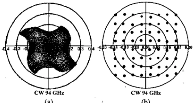
amplitude/phase states and minimize the amplitude imbalance and phase imbalance of the IQ modulator. The static constellation diagrams were obtained from CW- mode S-parameters measurement with a computer control
setup. The forward transmission coefficients at 94 GHz
control voltages of IP, IN, QP and QN have been swept
from 0 V to 4 V with step of 0.02 V. Based on forward
transmission coefficients, EVM calculation is used to extract the best amplitude and phase states. We can generate the static constellation diagrams of QPSK or higher order QAM modulations. We use 64-QAM as an example, to plot the extracted constellation diagram in Fig.
3(b), which features a minimum insertion loss of 14 dB,
amplitude imbalance of 1 dB and phase imbalance of I".
0
CW 94 GHz CW 94 GHz
(a) (b)
Fig. 3. The measured static constellation diagram of the HBT
IQ modulator at 94 GHz, (a) sweep I and Q control voltage with
a step of 0.02 V, (b) extracted 64-QAM.
The block diagram of the vector signal measurement
system is plotted in Fig. 4 for the millimeter-wave IQ
modulator. The H p 85105A millimeter-wave test set is
used to provide the carrier signal. The HP 11970-series
harmonic mixer and the HP 70000 spectrum analyzer are
used as a down-converter to convert millimeter-wave
signal to an IF frequency of 21.4 MHz. Finally, the 21.4-
MHz IF signal is fed into HP 89441A vector signal
analyzer for the analysis of the digital modulation quality.
Two HP 33120A arbitrary waveform generators are used
as the baseband IQ signal sources, which are controlled
with a computer and
HP
VEE software. The IQ sourcesare fed into a single-to-differential circuit network to
produce differentia1 IQ sources (IP, IN, QP and QN). For
channel power measurement, the
HF'
70000 spectrumanalyzer is replaced with the HP 8565EC spectrum
analyzer with built-in channel power measurement
software. The overall measurement system features
maximum operation frequency of 110 GHz, maximum
symbol rate of 2-Mps, maximum analysis bandwidth of 3
MHz and supports multiple digital modulation formats.
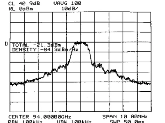
The measured output spectrum of QPSK modulation is
plotted in Fig. 5 and the output power is about -21.3 dBm
with a channel bandwidth of 2 MHz. The measured
QPSK modulation quality results at 94 GHz are plotted in
Fig. 6, including I-Q vector diagram, eye diagram, error
versus time plot and performance summaty. The LO
power is about -8 dBm and the amplitude of the baseband
IQ signal is 2-V,. The baseband IQ is coded with a
QPSK modulation format, a 2-Mhps data rate, pseudo random noise code.and the mapping table used with the extracted results fiom static constellation diagram measurement. For minimum the spectrum spread, we use
a root raised cosine (RRC) filter with a 0.5-avalue to
filter the baseband IQ signal. The measured EVM is
below 9.7 %, the amplitude error is below 7.3 % and the
phase error is below 3.7" in root-mean-square (RMS)
format.
The EVM degradation is due to the quadrature error and IQ imbalance within the IQ modulator. Additionally, the
imperfect LO/IQ sources in the test setup will also
degrade the EVM performance. For the W-band
applications, the phase noise and amplitude noise of the
LO source may result in 3-5 % EVM degradation, which
was analyzed with a THRU pad. The EVM analysis of
CW-mode LO source is like an all-0 data modulation
signal. On the other hand, the EVM may he degraded 3-4
% from the IQ sources, which was measured with a vector
signal analyzer. This EVM degradation from IQ sources is due to high data rate operation of the arbitrary waveform generators and the nonlinearity of the single-to- differential circuit network. The performance summary of the IQ modulator is summarized in Table I. As can he observed, this MMIC demonstrated wider bandwidth, low EVM degradation and good LO rejection. The success of
this chip development provides many potential
applications in millimeter-wave communication systems.
Fig.4. The block diagram of the vector signal
measurement system for the millimeter-wave IQ modulator.
IV. CONCLUSION
A broadband HBT IQ modulator and a vector signal
measurement system for millimeter-wave IQ modulator have been implemented and proposed in this paper. This IQ modulator MMIC is suitable for broadband digital modulated applications due to its wide bandwidth, low
insertion loss, low amplitudeiphase imbalance and good
inpuuoutput return loss. Also, this MMIC has been tested
and verified under the vector signal measurement
successfully. The vector signal measurement system
presented in this paper provides a dynamic signal test
bench for the IQ modulator. For the digital modulation
signals, the dynamic signal measurement is more Department of Education of Republic of China (ME-89-E-
meaningid than the static signal measurement. Therefore, FA06-24-6). The MMIC chip is fabricated by WIN
we can figure out the characteristic of the MMlC circuit Semiconductors. The authors would like to thank MI. G.
and the impairment coming from the imperfect signal G. Boll of GGB Inc. for his providing the W-hand probes
source. for chip on-wafer testing.
C L 4 0 9 d B UAUG 100
R L 0 d B m I 0 d W
CENTER 9 4 0 0 0 0 0 G H x SPRN 10 00MHz
RBW l 0 0 k H i UBW 100kHr SUP 5 0 0 m r
Fig. 5. The measured output spectrum of the HBT IQ
modulator is applied QPSK modulation format and the output
power is -21.3 dBm with a channel bandwidth of 2 MHz.
I -a aa / d i *
Fig. 6. The measured QPSK modulation quality results at 94
GHz, I-Q vector diagram, eye diagram, error vector versus time plot and performance summary.
Table I Performance Summary of the HBT IQ modulator
I10 GHz
Frcqucncy I50 GHa
I
60 GHaI
77 GHzI
94 GHzI
InsertionI
9 d BI
8dB1
9 d BI
14dBI
18dBI
I
I
I
I
*With calibration bias: #QPSK modulation with 2-Mps data rate
ACKNOWLEDGEMENT
This work is supported in part by National Science Council (NSC 89-2213-E-002-178 and NSC 90-2219-E-
002-007) and Research Excellence Program funded by
REFERENCES
[ I ] R. Desrosiers, et a / , “Monolithic 14 GHz widerhand InP
HBT BPSK modulator,” I998 Gallium Arsenide Integrated
Circuit Symposium, pp.135-138.
[2] Isahell Telliez, et al, “A compact monolithic microwave
demodulator-modulator for 64-QAM digital radio links,”
IEEE Trans. on Microwave Theory and Tech., vol. 39, no. 12, December, 1991, pp.1947-3954.
[3] G. Samuel Dow et al, ‘Vector signal measurement for 38
CHz dieital radio annlications.”
..
Microwave Journal.October,i999.
141 A. Alexanian. et al. “A SiGe transceiver ChiDset for 100
. _
Mbpdl Gbps digital communication over cable system,”
2002 IEEE Radio Freauencv Integrated
.
,
-
Circuits Symposium, pp.119-122.151 Andrew Weetzei. “A stable 250 to 4000 MHz GaAs IO
. _
modulator I C i I997 IEEE International Solid-Star;
Circuifs Conference, pp.364-365.
[6] Angel Boveda, Felix Orilgoso, Jose I. Alonso, “A 0.7-3 GHz
GaAs QPSWQAM direct modulator,” IEEE Journal of
Solid-State Circuits, vol. 28, no. 12 December, 1993, pp. 1340-1349.
[7] Dennis C. W. Lo, et 01, ‘Wove1 monolithic multifunctional
balanced switching low-noise amplifiers,” IEEE Trans. on
Microwave Theory and Tech., vol. 42, no. 12, December, 1994, pp.2629-2634.
[SI T. Lodhi, et al, “A 77 GHz coplanar waveguide MMIC
BPSK Vector Modulator realized using 1nP Technology,”
2000 IEEE GaAs ICSymposium Digest, pp.183-186.
[9] AliE. Ashtiani, et a/, “Direct multilevel carrier modulation
using millimeter-wave balanced vector modulators,” IEEE
Transactions on Microwave Theory and Techniques, vol. 46,
no. 12, December 1998,pp. 2611-2619.
[IO] S. Nam, et al, “Monolithic millimeter-wave balanced bi-
phase amplitude modulator in GaAsfinCaP HBT
technology,” I999 IEEE International Microwave
Symposium, vol. I , pp. 243-246.
[ I l l A.E. Ashtiani, e f al, “Monolithic GaAsiInGaF’ HBT
balanced vector modulator for millimeter-wave wireless
systems,” 2000 IEEE Radio Frequency Integrated Circuit
Symposium Digest, pp.187-190.
[I21 Hong-Yeh Chang, et a / , “A 45-90 GHz BPSK Modulator
Using HBT Technology”, 2002 Asia Pacific Microwave
Conference, Nov. 2002, Kyoto, Japan..
[I31 S . G. Dow, et al, “Vector signal characterization of 38 GHz
power amplifier with 100 Mbps QPSK modulation,” 2000
IEEE International Microwave Symposium, pp. 1847-1 850.
[I41 GaAs 1 vm HBT Model Handbook 1.0, WIN
Semiconductors Corp., July, 2001.
[IS] Sonnet User’s Manual, Release 6.0, Sonnet Software Inc.,
Liverpool, NY, April 1999.