國
國
國
國
立
立
立
立
交
交
交
交
通
通
通
通
大
大
大
大
學
學
學
學
電機學院
電機學院
電機學院
電機學院光電顯示
光電顯示
光電顯示科技產業研發碩士
光電顯示
科技產業研發碩士
科技產業研發碩士
科技產業研發碩士班
班
班
班
碩
碩
碩
碩
士
士
士
士
論
論
論
論
文
文
文
文
低溫複晶矽薄膜電晶體在閘極關閉區脈衝電壓及
低溫複晶矽薄膜電晶體在閘極關閉區脈衝電壓及
低溫複晶矽薄膜電晶體在閘極關閉區脈衝電壓及
低溫複晶矽薄膜電晶體在閘極關閉區脈衝電壓及
汲極直流偏壓下的劣化研究
汲極直流偏壓下的劣化研究
汲極直流偏壓下的劣化研究
汲極直流偏壓下的劣化研究
Study of LTPS TFTs Degradation under Gate Pulse Stress
in OFF Region with Drain Bias
研
研
研
研
究
究
究
究
生
生
生:
生
:林曉嫻
:
:
林曉嫻
林曉嫻
林曉嫻
Hsiao-Hsien Lin
指導教授
指導教授
指導教授
指導教授:
:戴亞翔
:
:
戴亞翔
戴亞翔
戴亞翔
博士
博士
博士
博士
Dr.Ya-Hsiang Tai
中
中
中
中
華
華
華
華
民
民
民
民
國
國
國
國
九
九十六
九
九
十六
十六
十六
年
年
年
年
十二
十二
十二
十二
月
月
月
月
低溫複晶矽薄膜電晶體在閘極關閉區脈衝電壓及
汲極直流偏壓下的劣化研究
Study of LTPS TFTs Degradation under Gate Pulse Stress
in OFF Region with Drain Bias
研 究 生:林曉嫻 Student:Hsiao-Hsien Lin
指導教授:戴亞翔 Advisor:Dr. Ya-Hsiang Tai
國 立 交 通 大 學
電機學院光電顯示科技產業研發碩士班
碩 士 論 文
A Thesis
Submitted to College of Electrical and Computer Engineering National Chiao Tung University
in partial Fulfillment of the Requirements for the Degree of
Master in
Industrial Technology R & D Master Program on Photonics and Display Technologies
December 2007
Hsinchu, Taiwan, Republic of China
低溫複晶矽薄膜電晶體在閘極
低溫複晶矽薄膜電晶體在閘極
低溫複晶矽薄膜電晶體在閘極
低溫複晶矽薄膜電晶體在閘極關閉區脈衝
關閉區脈衝
關閉區脈衝
關閉區脈衝
電壓
電壓
電壓
電壓及
及
及汲極直流偏壓下的劣化研究
及
汲極直流偏壓下的劣化研究
汲極直流偏壓下的劣化研究
汲極直流偏壓下的劣化研究
研究生
研究生
研究生
研究生:
:
:
:林曉嫻
林曉嫻
林曉嫻
林曉嫻
指導教授
指導教授:
指導教授
指導教授
:
:
:戴亞翔
戴亞翔
戴亞翔
戴亞翔
博士
博士
博士
博士
國立交通大學電機學院產業研發碩士班
國立交通大學電機學院產業研發碩士班
國立交通大學電機學院產業研發碩士班
國立交通大學電機學院產業研發碩士班
摘要
摘要
摘要
摘要
低溫複晶矽薄膜電晶體 (poly-Si TFTs) 與非晶矽薄膜電晶體 (a-Si TFTs) 相 比,具有較高的驅動電流,這是因爲電子在複晶矽的傳輸速度較快、膜品質也較優 良,因而可以使薄膜電晶體的尺寸更小,並增加顯示器的亮度及減少功率消耗。另 外,低溫多晶矽薄膜電晶體可在玻璃基板上嵌入驅動元件,並且大幅減少驅動 IC 的空間,更提升液晶顯示面板的特性及可靠度,使面板的製造成本降低,因此它的 發展將使顯示系統可以整合在玻璃基板上。然而,TFT 在系統面板中的電路之操作 是多樣而動態的;因此,為了保證產品的壽命,TFT 在這些操作條件的可靠度必須 加以探討。 在這篇論文中,我們排除了 overshooting 的效應,進一步研究了低溫複晶矽薄 膜電晶體在閘極 (gate) 關閉區脈衝電壓、及不同汲極 (drain) 直流偏壓下的劣化情 形。對 N-type TFTs 而言,當閘極電壓是在 ±15V 內操作、且源極 (source) 和汲極 端接地時,元件的劣化只會和閘極脈波下降的時間有關,和上升的時間不相關;但 是如果閘極交流電壓的操作範圍小於臨界電壓、又源極和汲極端接地時,元件的劣 化會同時和閘極脈波上升及下降的時間有關。對 P-type TFTs 而言,則是和 N-type
TFTs 劣化情形不同,當閘極電壓是在 ±15V 內操作、且源極和汲極端接地時,元件 的劣化只會和閘極脈波上升的時間有關,和下降的時間不相關;但是如果閘極電壓 的範圍是從 0V 掃到 15V、又源極和汲極端接地時,元件的劣化會和閘極脈波上升 及下降的時間皆不相關。 且根據實驗結果發現,對 N-type 和 P-type 在閘極關閉區脈衝電壓、汲極端加偏 壓的情形,劣化會隨著汲極端偏壓的加大而更趨嚴重,且源極和汲極會產生不同的 劣化行為。然而,P-type 不論在電流-電壓、還是電容-電壓曲線的劣化,都不如 N-type 明顯。同時元件的劣化也會和閘極電壓的範圍有關,而閘極電壓的上升時間 和下降時間效應,因為汲極端的偏壓會產生其他影響,使得上升時間和下降時間的 效應不明顯。
Study of LTPS TFTs Degradation under Gate
Pulse Stress in OFF Region with Drain Bias
Student:
:
:Hsiao-Hsien Lin Advisor:
:
:
:
:Dr. Ya-Hsiang Tai
Industrial Technology R & D Master Program of
Electrical and Computer Engineering College,
National Chiao Tung University
ABSTRACT
The driving current of panel of low temperature polycrystalline silicon thin film transistors (LTPS TFTs) is higher than the amorphous silicon thin film transistors (a-Si TFTs). The fast mobility in the good film of LTPS TFTs can make the size of TFTs small. Therefore, the display luminance can be increased and power consumption can be reduced. Furthermore, LTPS TFTs can be used to implement active circuits on single glass substrates and diminish spaces of active IC. It not only promotes the characteristic and reliability in liquid crystal display, but also comes down the manufacturing cost. So, it makes display systems with integrated circuit on the glass substrates to be feasible. However, the operation of the TFTs in the circuit of display system can be diverse and dynamic. Therefore, to insure the lifetime of the product, the reliability of TFTs under such kinds of operation conditions must be studied.
transistor under gate AC stress in off region with different drain bias has been investigated where the overshooting effect is prevented. For the N-type TFTs under the stress of gate voltage swinging from -15V to 15V with source and drain grounded, the device degradation depends on the falling time of gate pulse, but not on the rising time. However, under the stress of gate voltage lower than the threshold voltage, the degradation is dependent on both the rising time and falling time of the gate signal. For the P-type TFTs under the stress of gate voltage swinging from -15V to 15V with source and drain grounded, the device degradation depends on the rising time of gate pulse, but not on falling time. However, under the stress of gate voltage swinging from 0V to 15V, the degradation is independent of the rising time and falling time.
For the N-type and P-type TFTs under gate AC stress in off region with drain bias, the degradation becomes worse with increasing drain voltage. It results in different degradation behaviors near the source and drain regions. The I-V and C-V characteristic of P-type TFTs are not that much degraded than those of N-type TFTs. With the increase of the range of gate pulse, the degradation also increases. The applied drain voltage may introduce the effects of large electric field near the drain. In contrast, the effects of rising time and falling time are not obvious.
誌
誌
誌
誌
謝
謝
謝
謝
首先要感謝我的指導教授 戴亞翔博士,謝謝老師在求學的兩年期間提供豐富 的資源,讓我無後顧之憂的專心於研究中;以及在課業方面,總是詳細指導、且不 厭其煩地講解我不了解之處;而在做研究之餘,老師也不忘提醒大家做人處事的態 度,不論在言教還是身教,都給予我們最好的榜樣。在老師的帶領之下,實驗室時 常充滿和樂且溫馨的氣氛,也讓我身旁擁有共同努力的同伴們,回憶起碩士生活可 說是既充實又多采多姿。 謝謝士哲學長、彥甫學長,和隔壁實驗室的泓緯學長,在研究方面給予我很多 的指導,不管如何淺顯的問題都詳細地解釋;謝謝畢業的虹娟學姊、偉倫、育德、 晉煒,不論是在課業還是生活上都提供我不少寶貴的建議;謝謝畢業的學長:俊文、 振業;謝謝ㄧ起奮鬥的同學們:明憲、長龍、逸侑、誼明、勝昌;謝謝學弟妹:枷 彬、允翔、漢清、國珮、柏廷、紹文、騰瑞;謝謝隔壁實驗室的亞諭、建名、思維、 立煒,兩年的期間因為有大家的陪伴,擁有很多快樂的時光。 再來,謝謝給我許多指導和方向的奕宏學長,既亦師也亦友;謝謝親愛的姿瑤, 這一路上和我分享論文研究的經驗,且在各方面相互激勵,很幸運我擁有這樣的好 姊妹;也謝謝所有的好朋友們:銘成、曉倩、素惠、品蓉、羚榛、玟伶、明家、曉 妤、思詠、雅筑、品霓、永欣、玓玓…等,在我有點成果時和我一同分享、若有點 失意也總是給我打氣、陪伴在我身旁。 最後,感謝親愛的爸媽和哥哥。第一次離開家裡在外地唸書,因為有你們無微 不至的照顧,以及對我的支持及鼓勵,才有今日有所成長的我,希望論文研究成果 能讓你們感到欣慰和滿意,僅以此獻給你們:我最親愛的家人以及所有曾經幫助過 我的人,謝謝大家、我如今才能完成碩士學位。 林曉嫻 2007.12 於交通大學 筆
Contents
Abstract (Chinese)……..……….. i
Abstract (English)………...……….. iii
Acknowledgements……… v
Contents……….………. vi
Figure Captions………. vii
Table Captions……… xiv Chapter 1 Introduction……… 1
1.1 Overview of Low-Temperature Polycrystalline Silicon Thin Film Transistors. 1 1.2 Review of Degradation Model for TFT under AC Stress………... 3
1.3 Motivation……….. 7
1.4 Thesis Organization………
10
Chapter 2 Experimental Procedures……….. 12
2.1 Procedures of Fabrication of LTPS TFTs……… 12
2.2 Extraction Method of Device Parameters………... 14
2.3 C-V Measurements……….. 15
2.4 Stress Conditions………. 15
2.4.1 Gate Pulse Stress with Drain and Source Ground……….. 16
2.4.2 Gate Pulse Stress with Drain Bias and Source Ground……….. 19
Chapter 3 Degradation for Poly-Si TFT under Gate Pulse Stress with Drain and Source Ground……….. 21
3.1 Frequency Dependence……….. 21
3.2 Gate Voltage Leveling Dependence……… 24
3.3 Rising Time and Falling Time for Vg of ON and OFF Region……….. 27
3.4 Rising Time and Falling Time for Vg in the OFF Region……… 30
Chapter 4 Degradation for N-type Poly-Si TFT under Gate Pulse Stress with Drain Bias………... 33
4.1 Frequency Dependence……….. 33
4.2 Effect of Drain Bias……… 36
4.2.1 Vg in ON and OFF Region……… 36
4.3 Effect of Gate Voltage Range……… 47
4.4 Other Effects………. 53
4.4.1 Effect of Rising Time………
53
4.4.2 Effect of Falling Time……….. 60
4.5 Results and Discussions………. 66
4.6 Summary……… 69
Chapter 5 Degradation for P-type Poly-Si TFT under Gate Pulse Stress with Drain Bias……..……… 71
5.1 Effect of Drain Bias………
71
5.2 Effect of Gate Voltage Range………. 75
5.3 Other Effects………... 81
5.3.1 Effect of Rising Time………. 81
5.3.2 Effect of Falling Time……… 87
5.4 Results and Discussions……….. 93
5.5 Summary………. 95 Chapter 6 Conclusions……… 96 Reference………... 98 Vita……….…… 103
Figure Captions
Chapter 1 Introduction
Fig. 1-1 The block diagram of active matrix display……… 1Fig. 1-2 A schematic diagram for degradation model of the N-type TFT……. 5
Fig. 1-3 A schematic diagram for degradation model of the P-type TFT…….. 6
Fig. 1-4 Previous researches of LTPS TFT reliability……… 8
Fig. 1-5(a) the verification of output waveform with overshooting………….. 9
Fig. 1-5(b) the verification of output waveform without overshooting………. 9
Chapter 2 Experimental Procedures
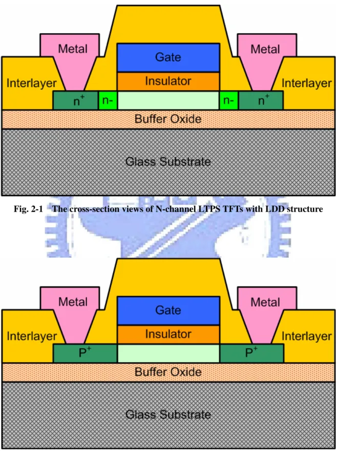
Fig. 2-1 The cross-section views of N-channel LTPS TFTs with LDD structure………. 13Fig. 2-2 The cross-section views of P-channel LTPS TFTs……….. 13
Fig. 2-3 Waveform and definition of the AC signal……….. 16
Fig. 2-4 TFT under AC stress with source and drain grounded………. 17
Chapter 3 Degradation for Poly-Si TFT under Gate Pulse Stress with
Drain and Source Ground
Fig. 3-1(a) Frequency dependence of degradation of N-channel TFT under gate pulse with drain and source ground……..……….. 22 Fig. 3-1(b) Frequency dependence of degradation of P-channel TFT under
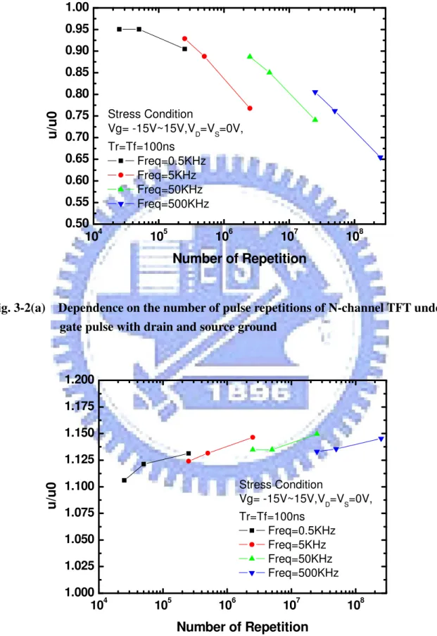
gate pulse with drain and source ground………..………….. 22 Fig. 3-2(a) Dependence on the number of pulse repetitions of N-channel TFT
under gate pulse with drain and source ground……….. 23 Fig. 3-2(b) Dependence on the number of pulse repetitions of P-channel TFT
under gate pulse with drain and source ground……….. 23 Fig. 3-3(a) Swing region for N-channel……… 24 Fig. 3-3(b) Dependence of degradation on swing region for N-channel TFT... 25 Fig. 3-4(a) Swing region for P-channel………. 26 Fig. 3-4(b) Dependence of degradation on swing region for P-channel TFT… 26 Fig. 3-5(a) Degradation of µ/µ0 in N-channel TFT under AC stress with
Vg = -15V to 15V measured for various rising times Tr and for
Tf = 100ns………. 27 Fig. 3-5(b) Degradation of µ/µ0 in N-channel TFT under AC stress with
Vg = -15V to 15V measured for various rising times Tf and for
Tr = 100ns………. 28 Fig. 3-6(a) Degradation of µ/µ0 in P-channel TFT under AC stress with
Vg = -15V to 15V measured for various rising times Tr and for
Tf = 100ns………. 29 Fig. 3-6(b) Degradation of µ/µ0 in P-channel TFT under AC stress with
Vg = -15V to 15V measured for various rising times Tf and for
Tr = 100ns………. 29 Fig. 3-7(a) Degradation of µ/µ0 in N-channel TFT under AC stress with
Vg = -15V to 0 V measured for various rising times Tr and for
Tf = 100ns………. 30 Fig. 3-7(b) Degradation of µ/µ0 in N-channel TFT under AC stress with
Vg = -15V to 0 V measured for various rising times Tf and for
Tr = 100ns………. 31 Fig. 3-8(a) Degradation of µ/µ0 in P-channel TFT under AC stress with
Vg = 0V to 15V measured for various rising times Tr and for
Tf = 100ns……….. 32 Fig. 3-8(b) Degradation of µ/µ0 in P-channel TFT under AC stress with
Vg = 0V to 15V measured for various rising times Tf and for
Chapter 4 Degradation for N-type Poly-Si TFT under Gate Pulse
Stress with Drain Bias
Fig. 4-1 TFT model in N-channel under Vg=-15V~15V and VD=20V with
different frequency……….. 33 Fig. 4-2(a) The frequency dependence of degradation of N-channel TFT under
Vg = -15V to 15V and VD=20V with the forward measurement…. 34
Fig. 4-2(b) The frequency dependence of degradation of N-channel TFT under Vg = -15V to 15V and VD=20V with the reverse measurement….. 35
Fig. 4-3(a) Forward dependence on the number of pulse repetitions of
N-channel TFT under Vg = -15V to 15V and VD=20V……… 35
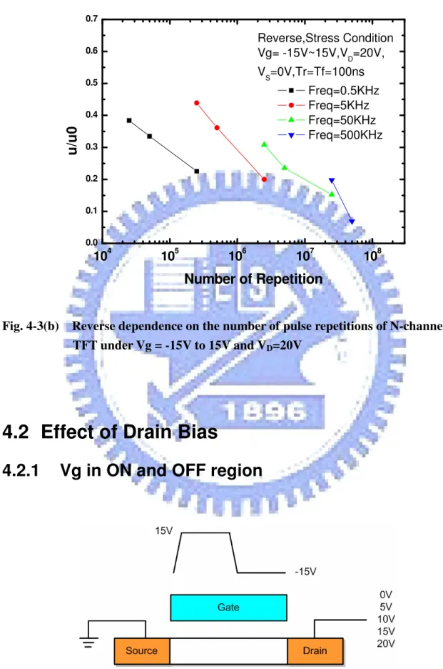
Fig. 4-3(b) Reverse dependence on the number of pulse repetitions of
N-channel TFT under Vg = -15V to 15V and VD=20V………….. 36
Fig. 4-4 TFT model in N-channel under various drain bias in on/off region…. 36 Fig. 4-5(a) Id-Vg forward curves before and after dynamic gate stress with
various drain bias in on/off region……… 37 Fig. 4-5(b) Dependence of the mobility on VDS with gate AC stress in
on/off region………. 38 Fig. 4-5(c) Dependence of the Sub-threshold Swing on VDS with gate
AC stress in on/off region………. 38 Fig. 4-6(a) Degradation of normalized CGS curve in N-channel under
various VDS in on/off region at frequency=1MHz………. 39
Fig. 4-6(b) Degradation of normalized CGD curve in N-channel under
various VDS in on/off region at frequency=1MHz……… 40
Fig. 4-7 TFT model in N-channel under various drain bias in off region…….. 40 Fig. 4-8(a) Id-Vg forward curves before and after dynamic gate stress with
various drain bias in off region………. 41 Fig. 4-8(b) Dependence of the mobility on VDS with gate AC stress in off
region……… 42 Fig. 4-8(c) Dependence of the Sub-threshold Swing on VDS with gate AC
stress in off region……….………. 42 Fig. 4-9(a) Degradation of normalized CGS curve in N-channel under
various VDS in off region at frequency=1MHz……… 43
Fig. 4-9(b) Degradation of normalized CGD curve in N-channel under
various VDS in off region at frequency=1MHz……… 44
Fig. 4-10(a) Forward saturation current under gate stress with various drain… 45 Fig. 4-10(b) Forward saturation current damage region model………. 45 Fig. 4-11(a) Reverse saturation current under gate stress with various drain… 46 Fig. 4-11(b) Reverse saturation current damage region model……….. 46
Fig. 4-12 TFT model in N-channel under various VDS and range of gate
voltage……….. 47 Fig. 4-13(a) Degradation of u/u0 in N-channel under various VDS and range
of gate voltage………...……….… 48 Fig. 4-13(b) Degradation of the sub-threshold swing in N-channel under
various VDS and range of gate voltage………...……..… 48
Fig. 4-14(a) Degradation of normalized CGS curve in N-channel
under Vg=-5V~0V with various VDS at frequency=1MHz…….. 49
Fig. 4-14(b) Degradation of normalized CGD curve in N-channel
under Vg=-5V~0V with various VDS at frequency=1MHz…….. 50
Fig. 4-15(a) Degradation of normalized CGS curve in N-channel
under Vg=-10V~0V with various VDS at frequency=1MHz…… 50
Fig. 4-15(b) Degradation of normalized CGD curve in N-channel
under Vg=-10V~0V with various VDS at frequency=1MHz……. 51
Fig. 4-16(a) Degradation of normalized CGS curve in N-channel
under Vg=-15V~0V with various VDS at frequency=1MHz……. 51
Fig. 4-16(b) Degradation of normalized CGD curve in N-channel
under Vg=-15V~0V with various VDS at frequency=1MHz…….. 52
Fig. 4-17(a) Degradation of normalized CGS curve in N-channel
under Vg=-20V~0V with various VDS at frequency=1MHz…….. 52
Fig. 4-17(b) Degradation of normalized CGD curve in N-channel
under Vg=-20V~0V with various VDS at frequency=1MHz…….. 53
Fig. 4-18 TFT model in N-channel under Vg=-15V~15V with changed
rising time Tr and fixed Tf………. 53 Fig. 4-19(a) Degradation of µ/µ0 in N-channel TFT under AC stress with
Vg = -15V to 15V measured for various rising times Tr and for
Tf = 700ns……… 54 Fig. 4-19(b) Degradation of S.S in N-channel TFT under AC stress with
Vg = -15V to 15V measured for various rising times Tr and for
Tf = 700ns……… 55 Fig. 4-20(a) Degradation of normalized CGS curve in N-channel under
Vg=-15V~15V measured for various Tr and for Tf = 700ns at
freq=1MHz……….. 56 Fig. 4-20(b) Degradation of normalized CGD curve in N-channel under
Vg=-15V~15V measured for various Tr and for Tf = 700ns at
freq=1MHz……… 56 Fig. 4-21 TFT model in N-channel under Vg=-15V~0V with changed
Fig. 4-22(a) Degradation of µ/µ0 in N-channel TFT under AC stress with
Vg = -15V to 0V measured for various rising times Tr and for
Tf = 700ns………. 58 Fig. 4-22(b) Degradation of S.S in N-channel TFT under AC stress with
Vg = -15V to 0V measured for various rising times Tr and for
Tf = 700ns……….. 58 Fig. 4-23(a) Degradation of normalized CGS curve in N-channel
under Vg=-15V~0V measured for various rising times Tr and for Tf = 700ns at freq=1MHz………. 59 Fig. 4-23(b) Degradation of normalized CGD curve in N-channel
under Vg=-15V~0V measured for various rising times Tr and for Tf = 700ns at freq=1MHz………. 60 Fig. 4-24 TFT model in N-channel under Vg=-15V~15V with changed
falling time Tf and fixed Tr……… 60 Fig. 4-25 Degradation of µ/µ0 in N-channel TFT under AC stress with
Vg = -15V to 0V measured for various falling times Tf and for
Tr = 700ns……… 61 Fig. 4-26(a) Degradation of normalized CGS curve in N-channel under
Vg=-15V~15V measured for various Tf and for Tr = 700ns
at freq=1MHz……….. 62 Fig. 4-26(b) Degradation of normalized CGD curve in N-channel under
Vg=-15V~15V measured for various Tf and for Tr = 700ns
at freq=1MHz……….. 63 Fig. 4-27 TFT model in N-channel under Vg=-15V~0V with changed
falling time Tf and fixed Tr……… 63 Fig. 4-28 Degradation of µ/µ0 in N-channel TFT under AC stress with
Vg = -15V to 0V measured for various falling times Tf and for
Tr = 700ns……… 64 Fig. 4-29(a) Degradation of normalized CGS curve in N-channel
under Vg=-15V~0V measured for various falling times Tf and for Tr = 700ns at freq=1MHz……….…………. 65 Fig. 4-29(b) Degradation of normalized CGD curve in N-channel
under Vg=-15V~0V measured for various falling times Tf and for Tr=700ns at freq=1MHz………..…….... 66 Fig. 4-30(a) The proposed AC stress degradation N-channel model
under VD=20V for various rising time Tr………. 67
Fig. 4-30(b) The time of electric field AC stress degradation N-channel
Fig. 4-31(a) The proposed AC stress degradation N-channel model
under VD=20V for various falling time Tf………... 68
Fig. 4-31(b) The time of electric field AC stress degradation N-channel
under VD=20V for various falling time Tf……….…….. 69
Chapter 5 Degradation for P-type Poly-Si TFT under Gate Pulse
Stress with Drain Bias
Fig. 5-1 TFT model in P-channel under various drain bias in off region…….. 71 Fig. 5-2(a) Dependence of the mobility on VDS with gate AC stress in off
region……….. 72 Fig. 5-2(b) Dependence of the Sub-threshold Swing on VDS with gate AC
stress in off region………..……. 72 Fig. 5-2(c) Dependence of the threshold voltage shift on VDS with gate AC
stress in off region……… 73 Fig. 5-3(a) Degradation of normalized CGS curve in P-channel under various
stress VDS in off region at frequency=1MHz……… 74
Fig. 5-3(b) Degradation of normalized CGD curve in P-channel under various
stress VDS in off region at frequency=1MHz……… 75
Fig. 5-4 TFT model in P-channel under various VDS and range of
gate voltage……….. 75 Fig. 5-5 Degradation of u/u0 in P-channel under various VDS and range of gate
voltage……….…. 76 Fig. 5-6(a) Degradation of normalized CGS curve in P-channel under
Vg=0V~5V with various VDS at frequency=1MHz……….… 77
Fig. 5-6(b) Degradation of normalized CGD curve in P-channel under
Vg=0V~5V with various VDS at frequency=1MHz…………...…. 78
Fig. 5-7(a) Degradation of normalized CGS curve in P-channel under
Vg=0V~10V with various VDS at frequency=1MHz……….. 78
Fig. 5-7(b) Degradation of normalized CGD curve in P-channel under
Vg=0V~10V with various VDS at frequency=1MHz……….. 79
Fig. 5-8(a) Degradation of normalized CGS curve in P-channel under
Vg=0V~15V with various VDS at frequency=1MHz……….. 79
Fig. 5-8(b) Degradation of normalized CGD curve in P-channel under
Vg=0V~15V with various VDS at frequency=1MHz……….. 80
Fig. 5-9(a) Degradation of normalized CGS curve in P-channel under
Vg=0V~20V with various VDS at frequency=1MHz……….. 80
Fig. 5-9(b) Degradation of normalized CGD curve in P-channel under
Vg=0V~20V with various VDS at frequency=1MHz……….. 81
rising time Tr and fixed Tf……….... 81 Fig. 5-11 Degradation of µ/µ0 in P-channel TFT under AC stress with
Vg = -15V to 15V measured for various rising times Tr and for Tf = 700ns……….. 82 Fig. 5-12(a) Degradation of normalized CGS curve in P-channel under
Vg=-15V~15V measured for various Tr and for Tf = 700ns at
freq=1MHz……… 83 Fig. 5-12(b) Degradation of normalized CGD curve in P-channel under
Vg=-15V~15V measured for various Tr and for Tf = 700ns at
freq=1MHz………...…. 84 Fig. 5-13 TFT model in P-channel under Vg=0V~15V with changed
rising time Tr and fixed Tf………. 84 Fig. 5-14 Degradation of µ/µ0 in P-channel TFT under AC stress with
Vg = 0V to 15V measured for various rising times Tr and for
Tf = 700ns……….. 85 Fig. 5-15(a) Degradation of normalized CGS curve in P-channel under
Vg=0V~15V measured for various Tr and for Tf = 700ns at
measuring freq=1MHz……….. 86 Fig. 5-15(b) Degradation of normalized CGD curve in P-channel under
Vg=0V~15V measured for various Tr and for Tf = 700ns at
measuring freq=1MHz……….. 87 Fig. 5-16 TFT model in P-channel under Vg=-15V~15V with changed
falling time Tf and fixed Tr……….. 87 Fig. 5-17 Degradation of µ/µ0 in P-channel TFT under AC stress with
Vg = -15V to 15V measured for various falling times Tf and for
Tr = 700ns………..… 88 Fig. 5-18(a) Degradation of normalized CGS curve in P-channel under
Vg=-15V~15V measured for various Tf and for Tr = 700ns at
freq=1MHz……… 89 Fig. 5-18(b) Degradation of normalized CGD curve in P-channel under
Vg=-15V~15V measured for various Tf and for Tr = 700ns at
freq=1MHz……….. 90 Fig. 5-19 TFT model in P-channel under Vg=0V~15V with changed
falling time Tf and fixed Tr……….. 90 Fig. 5-20 Degradation of µ/µ0 in P-channel TFT under AC stress with
Vg = 0V to 15V measured for various falling times Tf and for
Tr = 700ns……….. 91 Fig. 5-21(a) Degradation of normalized CGS curve in P-channel under
Vg=0V~15V measured for various Tf and for Tr = 700ns at
freq=1MHz………. 92
Fig. 5-21(b) Degradation of normalized CGD curve in P-channel under
Vg=0V~15V measured for various Tf and for Tr = 700ns at
freq=1MHz……….... 92 Fig. 5-22 Schematic illustration of the mechanism causing the
hot-electron-induced- punchthrough effect……….. 93 Fig. 5-23(a) The degradation model in the forward Id-Vg measurement…….... 94 Fig. 5-23(b) The degradation model in the reverse Id-Vg measurement……… 94 Fig. 5-24 The C-V degradation model under a large drain bias………... 95
Table Captions
Chapter 2 Experimental Procedures
Table 2-1 The experiment condition forms for N-type under gate pulse with drain and source ground………. 18 Table 2-2 The experiment condition forms for P-type under gate pulse with drain
and source ground……… 18 Table 2-3 The experiment condition forms for N-type under gate pulse with drain
bias and source ground……….... 20 Table 2-4 The experiment condition forms for P-type gate pulse with drain bias
and source ground……… 20
Chapter 6 Conclusions
Table 6-1 Summary statement of rising time and falling time dependence of gate AC signal for N-type………...…………. 97 Table 6-2 Summary statement of rising time and falling time dependence of gate
Chapter 1
Introduction
1.1 Overview of Low-Temperature Polycrystalline
Silicon Thin Film Transistors ( LTPS TFTs )
Nowadays, the amorphous silicon (a-Si) thin film transistors (TFTs) are commonly used to be the switches of the pixel in active matrix liquid crystal displays (AMLCDs). Fig. 1-1 shows the block diagram of active matrix display. All the driver chips are buried together with the other application-specified ICs on PCB because the current driving capacity of a-Si TFTs is not good enough for the system integration. However, the integration of driver circuitry with display panel on the same substrate is very desirable not only to reduce the module cost but to improve the system reliability.
For this reason, low-temperature polycrystalline silicon (poly-Si) thin film transistors (TFTs) have attracted much attention because they have been used very successfully for active matrix displays, such as active matrix liquid crystal displays (AMLCDs) and active matrix organic light emitting displays (AMOLEDs). Except large area displays, poly-Si TFTs have been applied into some memory device such dynamics random access memories (DRAMs), static random access memories (SRAMs), and have great potential for 3-dimension IC applications.
Compared with conventional a-Si TFTs, the field effect mobility of poly-Si TFTs is much higher. In polysilicon film, the carrier mobility larger than 100cm2/Vs can be
easily achieved, which is about 100 times larger than that of the conventional amorphous-silicon TFTs (typically below 1cm2/Vs). Higher field effect mobility means
transistors can provide higher driving current. The higher driving currents can allow the pixel-switching element TFT’s dimension shrinkage, resulting in higher aperture ratio and lower parasitic gate-line capacitance for improved display performance. Besides, the superior mobility performance allows the integration of both the active matrix pixel switching elements and the peripheral driving circuitry on the same glass substrate, which brings the era of system-on-glass (SOG) that will include a memory, central processing unit (CPU), and display on the same glass. In this way, the process complexity can be greatly simplified and manufacturing cost can be substantially reduced. The ability of fabricating high-performance low temperature poly-Si (LTPS) TFTs enables their use in a wide range of new applications. Therefore, there is a great interest in improving the performance of LTPS TFTs.
In comparison with signal-crystalline silicon, poly-Si film contains many grain boundary defects and intra-grain defects. The order of poly-Si grain size is about 0.3um. At present, when poly-Si TFTs are used in LCD applications, the minimum channel length is typically much larger than 3µm, and therefore a large number of grain boundaries are
present in the channel. Electrons are scattered at the grain boundaries or trapped by the interface states, leading to lower mobility than in single crystal silicon. Much effort has been made to increase the performance of LTPS TFTs. Crystallization of a-Si thin films has been considered the most critical process for fabricating high-performance LTPS TFTs. Among various crystallization technologies, excimer laser crystallization has become the mainstream technology for mass production of flat panel displays (FPDs) because of high throughput, low temperature process compatible with glass substrate, and formation of high-quality poly-Si.
In summary, it is expected that the poly-Si TFTs will become increasingly important in future technology, especially when the 3-D circuit integration and SOG era is coming. There are lots of interesting and important topics that are worthy to be researched.
1.2 Review of Degradation Model for TFT under
AC Stress
In order to realize the new applications for LTPS TFTs, we have to improve the performance such as enhancing mobility, decreasing the threshold voltage of TFTs, and shrinking the TFTs size. However, the poly-Si TFT reliability improvements are as critical for the insurance of product lifetime. Therefore, reliability testing and understanding of reliability mechanisms become very necessary.
In previous reports, Toyota et al. proposed that mobile carriers are able to follow the transient variation of gate voltage while the electrons trapped in the midgap state aren’t. In addition, Uraoka et al. attributed the dominant AC degradation mechanism to hot electrons generated by trapped electrons exposed to the high electric field and gain energy from the electric field during AC stress. The mechanism was analyzed by using a pico-second
emission microscope and device simulation to examine the transient current experimentally and theoretically, respectively.
The earlier degradation model under AC stress is described as follow. As for the N-type TFTs, when the gate voltage is high of Vg=15V (ON state), the electrons gather to form a channel, as shown in Fig. 1-2 (a). When the gate voltage drops from Vg=15V to -15V (ON→OFF), the electrons in the channel move rapidly to the source and drain, as shown in Fig. 1-2 (b). Some of the trapped electrons are exposed to the high electric field and gain energy from the field. Hot electrons are generated at this moment and form electron traps, as shown in Fig. 1-2 (c), and a density of state (DOS) in tail edge of poly-Si is increased by the hot electrons.
As for the P-type TFTs, when the gate voltage is low of Vg=-15V (ON state), the holes gather to form a channel, as shown in Fig. 1-3 (c). When the voltage transition from low to high of Vg=-15V to 15V (ON→OFF), the holes in the channel move rapidly to the source and drain, as shown in Fig. 1-3 (b). Carriers gain energy from this electric field and become hot carriers. Therefore, more hot electrons are generated which causes trap formation at the grain boundaries around the drain edge, as shown in Fig. 1-3 (a).
ON High (Vg=+15V) Low (Vg=-15V) OFF channel (low field) depletion (high field) Vg=+15V channel formation channel Vth
(a)
ON High (Vg=+15V) Low (Vg=-15V) OFF channel (low field) depletion (high field) Vg=+15V -15Vgeneration of hot carrier current
Vth
(b)
ON High (Vg=+15V) Low (Vg=-15V) OFF channel (low field) depletion (high field) Vg=-15Vgeneration of electron traps
Vth
(c)
Vg=+15V
generation of electron traps
Vth
(a)
channel (low field) depletion (high field) Low (Vg=-15V) ON OFF High (Vg=+15V) Vg=-15V +15Vgeneration of hot carrier current
Vth
(b)
channel (low field) depletion (high field) OFF High (Vg=+15V) Low (Vg=-15V) ON Vg=-15V channel formation channel Vth(c)
channel (low field) depletion (high field) OFF High (Vg=+15V) Low (Vg=-15V) ON1.3 Motivation
The Poly-Si TFTs displays with integrated driving circuits have recently been developed. At present, the poly-Si TFTs are the best candidate to realize system on panel (SOP) and are widely considered for AMLCDs and active matrix organic light-emitting diodes (AMOLEDs).
The reliability mechanisms of LTPS TFTs under DC (direct current) bias stress and AC stress which source drain were ground have been widely discussed. However, up to now, the reliability of LTPS TFTs under gate AC stress with drain bias has been paid much less attention, shown in Fig. 1-4. In previous studies regarding AC stress, the source and drain were ground to avoid the DC effect during dynamic stress. However, when the gate of the TFT is under dynamic operation, the drain-source voltage is usually present. For example, the pixel TFTs driven by multi level gate scanning waveforms can be subject to the off-region AC stress at gate with DC drain bias.
Last, CMOS technology is necessary for driving circuits, which means that both the understanding of the reliability of N-type and P-type LTPS TFTs are necessary. Therefore, it is extremely important to understand the degradation mechanisms of N-channel and P-channel LTPS TFTs under AC stress.
Fig. 1-4 Previous researches of LTPS TFT reliability
For the previous work in our lab (thesis of Wei-Lun Shih), it is not noticed that the applied gate signals overshoot beyond the target value we have set. Based on those results, it is found that the signal of Vgh is higher and Vgl is lower than the values we set, as shown in Fig. 1-5(a). The effect of overshooting could introduce other effect of the study of reliability.
Therefore, in this study, the overshooting is carefully avoided for the applied gate signals, as shown in Fig. 1-5(b). The degradation behavior can be free from the overshooting effect. Thus, we re-examine the degradation of N-channel and P-channel LTPS TFTs under off-region AC stress conditions with various drain bias with proper apparatus setup. The stress conditions including swing range, and falling/rising times of the gate pulse, were discussed to verify the degradation mechanism under gate AC stress
with drain bias.
Fig. 1-5(a) the verification of output waveform with overshooting
1.4 Thesis Organization
Chapter 1
Introduction
1.1 Overview of Low-Temperature Polycrystalline Silicon Thin Film Transistors (LTPS TFTs)
1.2 Review of Degradation Model for TFT under AC Stress 1.3 Motivation
1.4 Thesis Organization
Chapter 2 Experimental Procedures
2.1 Procedures of Fabrication of LTPS TFTs 2.2 Extraction Method of Device Parameters 2.3 C-V Measurements
2.4 Stress Conditions
2.4.1 Gate Pulse Stress with Drain and Source Ground 2.4.2 Gate Pulse Stress with Drain Bias and Source Ground
Chapter 3
Degradation for Poly-Si TFT under Gate Pulse Stress with
Drain and Source Ground
3.1 Frequency Dependence
3.2 Gate Voltage Leveling Dependence
3.3 Rising Time and Falling Time for Vg of ON and OFF Region 3.4 Rising Time and Falling Time for Vg in the OFF Region
Chapter 4
Degradation for N-type Poly-Si TFT under Gate Pulse Stress
4.1 Frequency Dependence 4.2 Effect of Drain Bias
4.2.1 Vg in ON and OFF region 4.2.2 Vg in the OFF region 4.3 Effect of Gate Voltage Range 4.4 Other Effects
4.4.1 Effect of Rising Time 4.4.2 Effect of Falling Time 4.5 Results and Discussions 4.6 Summary
Chapter 5
Degradation for P-type Poly-Si TFT under Gate Pulse Stress
with Drain Bias
5.1 Effect of Drain Bias
5.2 Effect of Gate Voltage Range 5.3 Other Effects
5.3.1 Effect of Rising Time 5.3.2 Effect of Falling Time 5.4 Results and Discussions 5.5 Summary
Chapter 2
Experimental Procedures
2.1 Procedures of Fabrication of LTPS TFTs
LTPS TFTs used in the experiment were the conventional top-gate structure and fabricated on the glass substrates. The cross-section views of N-channel and P-channel LTPS TFTs are shown in Fig 2-1 and Fig. 2-2 respectively. The basic process flow is described as follows. Firstly, the buffer oxide and a-Si:H films were deposited on glass substrates by the PECVD system. Then, XeCl excimer laser was used to crystallize a-Si:H film followed with poly-Si active area definition. Subsequently, gate insulator was deposited by PECVD. The thickness of gate oxide is 650Å. Next, the metal gate formation and source/drain doping were performed. Dopant activation and hydrogenation was carried out after interlayer dielectric deposition. Finally, contact holes formation and metallization were performed to complete fabrication work. The lightly doped drain (LDD) structure was used in the N-channel TFTs to enhance hot carrier endurance while not used in P-type devices. The width/length of the TFT was 20μm/5μm.
Fig. 2-1 The cross-section views of N-channel LTPS TFTs with LDD structure
2.2 Extraction Method of Device Parameters
The field effect mobility (Mu, µFE) is derived from the maximum value of the
transconductance gm, which can be expressed as:
2 1 [( ) ] 2 D FE ox G th D D W I C V V V V L µ = − − (2-1) Where
Cox is the gate capacitance per unit area,
W is channel width, L is channel length,
Vth is the threshold voltage.
If the drain voltage VD is much smaller as compared with (VG−Vth) (i.e. VD << VG -
Vth), then the drain current can be approximated as:
D TH G ox FE D V V V L W C I =µ ( − ) And the transconductance is defined as:
D FE ox const V G D m
V
L
WC
V
I
g
Dµ
=
∂
∂
=
= . (2-3)Therefore, the field effect mobility can be expressed as:
m
g
FE ox DL
C W V
µ
=
(2-4)In other words, the field-effect mobility can be extracted by taking the maximum value of the gm into (2-4) when VD = 0.1V.
For most of the researches on TFT, the constant current method is widely-used to determine the threshold voltage (Vth). The threshold voltage in the thesis is determined
from this method, which extracts Vth from the gate voltage at the normalized drain current
N D eff eff
I =I /(W -L )=10nA for |VDS|=0.1V.
2.3 C-V Measurements
Since the I-V transfer curves show the entire characteristics of the whole channel and may not distinguish the dominant mechanism, C-V measurements were further employed to investigate the asymmetry electric field at the source and drain of TFTs during the stress.
The C-V curves of the normalized gate-to-drain capacitance (CGD) and the normalized
gate-to-source capacitance (CGS) before and after stress at different stress conditions were
measured with the Agilent 4284Aprecision LCR meter. The normalized capacitance is the ratio of the measured capacitance to a constant of 60fF, which is the gate oxide capacitance of the TFT under test.
Since it is difficult to observe the defect position in TFTs with the I-V characteristic, the C-V measurement is used to examine the information about position and type of degradation in the device after stress. For instance, if carriers are trapped by defects, C-V curve stretch out slightly, or if states are generated additionally, C-V curve increase somewhat in the depletion region. Besides, the C-V curves are helpful to identify whether the dominant mechanism of degradation is the increase of fixed charges or trap states.
2.4 Stress Conditions
The Agilent 4156A semiconductor parameter analyzer with pulse generator was used to measure the I-V curve and stress the device with different conditions. The basic parameters of AC signal consists of frequency (F), signal high level (Vgh), signal low level (Vgl), high-level time (T_Vgh), low-level time (T_Vgl), rising time (Tr), and falling time (Tf). Fig 2-3 shows the waveform of the AC signal. In AC signal, the definition of individual parameter is given as above:
T = Tr + T_vgh + Tf + T_vgl (2-5) F = 1/T Duty ratio = (Tr + T_vgh)/T (2-7) where T is the signal period.
Fig. 2-3 Waveform and definition of the AC signal
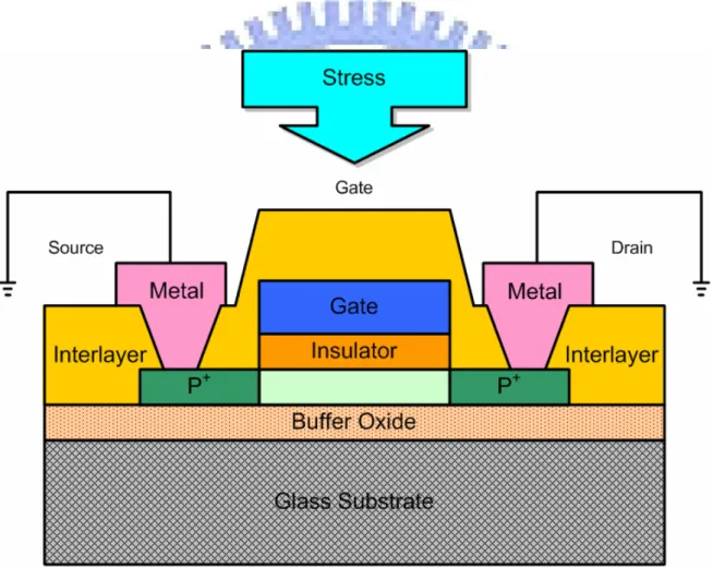
2.4.1 Gate Pulse Stress with Drain and Source Ground
Under AC stress, pulse voltage was applied to the gate electrode and source and drain were grounded, which is shown in Fig. 2-4. The standard stress condition in the experiment is the gate voltage swing of -15V to 15V, F = 500 kHz, Tr and Tf are both 100ns, and duty ratio is 50%. These parameters can be adjusted and then various stress conditions on the gate electrode were performed to examine the reliability of LTPS TFTs.
To investigate which parameter of the stress parameters dominates the degradation of the N-channel and P-channel TFTs transfer characteristics, we will make four experiments. (2-6)
Firstly, we change frequency from 0.5KHz to 500KHz. Secondly, we change Vgh and Vgl of AC signal fixed amplitude of 15V at one time, called Vg leveling. Thirdly, we will change Tr and Tf from 100ns to 700ns for gate swing range of -15V to 15V. And finally, we want to understand the effects of Tr and Tf for the gate swing in the depletion region. The experimental conditions are shown in Table 2-1 and Table 2-2. It will be investigated for reliability testing in the chapter 3.
Table 2-1 The experiment condition forms for N-type under gate pulse with drain and source ground
Table 2-2 The experiment condition forms for P-type under gate pulse with drain and source ground
2.4.2 Gate Pulse Stress with Drain Bias and Source
Ground
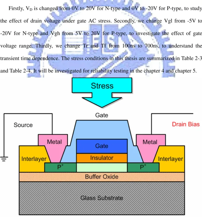
In the second part of experiment, pulse voltage was applied to the gate electrode in off region with drain DC while source is grounded, which is shown in Fig. 2-5. The standard stress condition in the experiment includes the gate voltage swing of -15V to 0V for N-type, 0V to 15V for P-type, F = 500 kHz, Tr and Tf are both 100ns, and duty ratio is 50%. These parameters can be adjusted to perform then various stress conditions.
Firstly, VD is changed from 0V to 20V for N-type and 0V to -20V for P-type, to study
the effect of drain voltage under gate AC stress. Secondly, we change Vgl from -5V to -20V for N-type and Vgh from 5V to 20V for P-type, to investigate the effect of gate voltage range. Thirdly, we change Tr and Tf from 100ns to 700ns, to understand the transient time dependence. The stress conditions in this thesis are summarized in Table 2-3 and Table 2-4. It will be investigated for reliability testing in the chapter 4 and chapter 5.
Table 2-3 The experiment condition forms for N-type under gate pulse with drain bias and source ground
Table 2-4 The experiment condition forms for P-type gate pulse with drain bias and source ground
Chapter 3
Degradation for Poly-Si TFT under Gate
Pulse Stress with Drain and Source
Ground
3.1 Frequency Dependence
Dependence of the device degradation on frequency for N-channel and P-channel TFT is shown in Fig. 3-1(a) and Fig. 3-1(b). The degradation are respectively expressed as the ratio of increased and decreased mobility (µ) for N and P-channel TFTs to their initial mobility (µ0). µ0 and µ are derived from the maximum transconductance at the drain
voltage of 0.1 V (N-channel) and -0.1V (P-channel) before and after stress. For N-channel TFT, when the frequency increases from 0.5KHz to 500KHz, the mobility decreases. For P-channel TFT, when the frequency increases, the mobility slightly increases.
The changes are re-plotted with the number of pulses for N-channel and P-channel TFT , as shown in Fig. 3-2(a) and Fig. 3-2 (b). Independent of the frequency, the degradation of all lines exhibits almost the universal relationship with the number of pulses. The figure clearly indicates the relationship between the degradation and the repetition number and the independence of the frequency. In other words, the degradation arisen by the unchanging voltage can be ignored.
0.1 1 10 100 1000 0.60 0.65 0.70 0.75 0.80 0.85 0.90 0.95 1.00
u
/u
0
Stress Time(sec)
Stress Condition Vg= -15V~15V,VD=VS=0V, Tr=Tf=100ns Freq=0.5KHz Freq=5KHz Freq=50KHz Freq=500KHzFig. 3-1(a) Frequency dependence of degradation of N-channel TFT under gate pulse with drain and source ground
0.1 1 10 100 1000 0.98 1.00 1.02 1.04 1.06 1.08 1.10 1.12 1.14 1.16
u
/u
0
Stress Time(s)
Stress Condition Vg= -15V~15V,VD=VS=0V, Tr=Tf=100ns Freq=0.5KHz Freq=5KHz Freq=50KHz Freq=500KHzFig. 3-1(b) Frequency dependence of degradation of P-channel TFT under gate pulse with drain and source ground
104 105 106 107 108 0.50 0.55 0.60 0.65 0.70 0.75 0.80 0.85 0.90 0.95 1.00 Stress Condition Vg= -15V~15V,VD=VS=0V, Tr=Tf=100ns Freq=0.5KHz Freq=5KHz Freq=50KHz Freq=500KHz
u
/u
0
Number of Repetition
Fig. 3-2(a) Dependence on the number of pulse repetitions of N-channel TFT under gate pulse with drain and source ground
104 105 106 107 108 1.000 1.025 1.050 1.075 1.100 1.125 1.150 1.175 1.200
u
/u
0
Number of Repetition
Stress Condition Vg= -15V~15V,VD=VS=0V, Tr=Tf=100ns Freq=0.5KHz Freq=5KHz Freq=50KHz Freq=500KHz3.2 Gate Voltage Leveling Dependence
The range of the gate pulse swing is separated into two parts according to the threshold voltage, as shown in Fig. 3-3(a) and Fig. 3-4(a). In the ON region, the channel is formed, while in the OFF region, the channel was fully depleted. Fig. 3-3(b) and Fig. 3-4(b) clearly indicates that the degradation of mobility strongly depends on the levels of the gate voltage. For the gate pulse swing in the ON region, the degradation is very small, however, that for the gate pulse swing fully in the OFF region become large. It is because the transient electrical field is high in the OFF region, but that is very low in the ON region. Carriers can gain energy from high electrical field and become hot carriers, and the traps are generated.
Fig. 3-4(a) Swing region for P-channel
3.3 Rising Time and Falling Time for Vg of ON and
OFF Region
For N-channel TFT, the transient time dependence for the degradation was examined as shown in Fig. 3-5. During the variation of rising time Tr from 100ns to 700ns with a fixed Tf of 100ns, no significant change in µ/µ0 was observed as shown in Fig. 3-5(a). On
the contrary, the degradation depended strongly on the falling time Tf as shown in Fig. 3-5(b). The degradation is remarkably accelerated with the decrease of the falling time from 700ns for 100ns for a fixed Tr of 100ns. In the case of changing rising time, the gate voltage varies from OFF region to ON region, and the mobile carriers are sited at so low electrical field that no device degradation is formed. But in the case of changing falling time, the gate voltage varies from ON region to OFF region, some carries remain in the channel and are subjected to the high electrical field becoming hot carries.
Fig. 3-5(a) Degradation of µ/µµ/µµ/µµ/µ0000 in N-channel TFT under AC stress with Vg = -15V to
Fig. 3-5(b) Degradation of µ/µµ/µµ/µµ/µ0000 in N-channel TFT under AC stress with Vg = -15V to
15V measured for various rising times Tf and for Tr = 100ns.
For P-channel TFT, the transient time dependence for the degradation was also studied. The dependence of the mobility change on rising time and falling time is shown in Fig. 3-6(a) and Fig. 3-6(b), respectively. The change was accelerated for a variation in rising time; however, the change was not affected by the falling time. In the case of changing rising time, the gate voltage varies from ON region to OFF region, and some carriers are sited at so high electrical field that device degradation is formed. But in the case of changing falling time, the gate voltage varies from OFF region to ON region; carriers are sited at low electrical field not becoming hot carries.
Fig. 3-6(a) Degradation of µ/µµ/µµ/µµ/µ0000 in P-channel TFT under AC stress with Vg = -15V to
15V measured for various rising times Tr and for Tf = 100ns.
3.4 Rising Time and Falling Time for Vg in the OFF
Region
We have known that degradation by pulse swing for the ON region was very small, however, that by pulse swing for the OFF region was large. We have already observed the transient time dependence for the degradation under AC stress with Vg = -15V to 15V. For this gate swing of N-channel TFT, it can be taken as steps of Vg = -15V to 0V (OFF region) and Vg =0V to 15V (ON region). Because no device degradation is formed for N-channel TFT under AC stress with Vg = 0V to 15V, we are only interested in the transient time dependence for the degradation of N-channel TFT at Vg = -15 V to 0V. For the gate voltage swings from -15V to 0V, it is firstly observed that the degradation is obviously dependent on both the rising time and falling time, as shown in Fig. 3-7(a) and Fig. 3-7(b). Since there are no induced electrons for these applied gate voltages, it reveals that the previously proposed model may be incomplete.
Fig. 3-7(a) Degradation of µ/µµ/µµ/µµ/µ0000 in N-channel TFT under AC stress with Vg = -15V to
Fig. 3-7(b) Degradation of µ/µµ/µµ/µµ/µ0000 in N-channel TFT under AC stress with Vg = -15V to
0 V measured for various rising times Tf and for Tr = 100ns.
For P-channel TFT, Vg = 0V to 15V is OFF region, and Vg =-15V to 0V is ON region. Because no device degradation is formed for P-channel TFT under AC stress with Vg =-15V to 0V, we are also only interested in the transient time dependence for the degradation of P-channel TFT at Vg = 0V to 15V. For the gate voltage swings from 0V to 15V, it is observed that the degradation is independent on the rising time and falling time, which is different from P-channel TFT under AC stress with Vg =-15V to 15V, as shown in Fig. 3-8(a) and Fig. 3-8(b).
Fig. 3-8(a) Degradation of µ/µµ/µµ/µµ/µ0000 in P-channel TFT under AC stress with Vg = 0V to
15V measured for various rising times Tr and for Tf = 100ns.
Chapter 4
Degradation for N-type Poly-Si TFT under
Gate Pulse Stress with Drain Bias
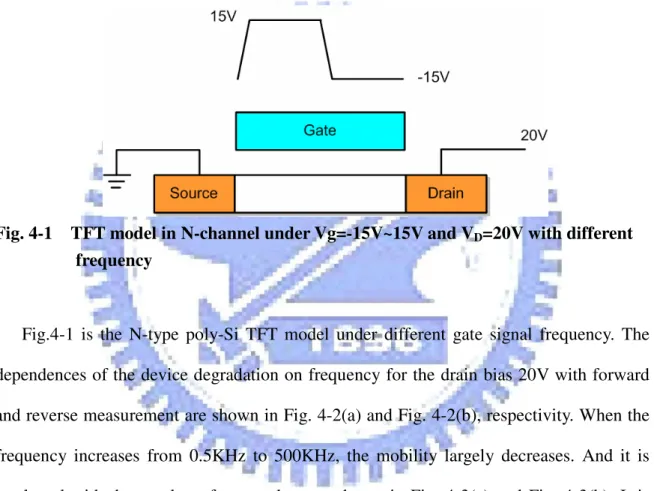
4.1 Frequency Dependence
Fig. 4-1 TFT model in N-channel under Vg=-15V~15V and VD=20V with different
frequency
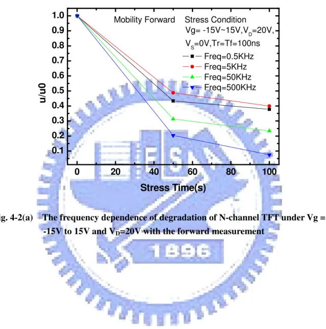
Fig.4-1 is the N-type poly-Si TFT model under different gate signal frequency. The dependences of the device degradation on frequency for the drain bias 20V with forward and reverse measurement are shown in Fig. 4-2(a) and Fig. 4-2(b), respectivity. When the frequency increases from 0.5KHz to 500KHz, the mobility largely decreases. And it is re-plotted with the number of gate pulses, as shown in Fig. 4-3(a) and Fig. 4-3(b). It is expected all lines exhibit the universal relationship in the equivalent repetition number as in the case of VD=0V. However, the data are different from what we expect. The
degradation of mobility u/u0 is not continuous for the case of VD=20V. The degradation in
the period with unchanged Vg can no longer be ignored. When the gate voltage is at 15V and the drain is biased at 20V, the TFT will suffer from the DC stress with large drain current, which makes the phenomena more complicated. The degradation of TFTs under
such an ON region AC gate stress will be further studied and not discussed in detail in this thesis. 0 20 40 60 80 100 0.1 0.2 0.3 0.4 0.5 0.6 0.7 0.8 0.9 1.0
u
/u
0
Stress Time(s)
Mobility Forward Stress Condition Vg= -15V~15V,V D=20V, VS=0V,Tr=Tf=100ns Freq=0.5KHz Freq=5KHz Freq=50KHz Freq=500KHz
Fig. 4-2(a) The frequency dependence of degradation of N-channel TFT under Vg = -15V to 15V and VD=20V with the forward measurement
0 20 40 60 80 100 0.1 0.2 0.3 0.4 0.5 0.6 0.7 0.8 0.9 1.0
Mobility Reverse Stress Condition
Vg= -15V~15V,VD=20V, V S=0V,Tr=Tf=100ns Freq=0.5KHz Freq=5KHz Freq=50KHz Freq=500KHz
u
/u
0
Stress Time(s)
Fig. 4-2(b) The frequency dependence of degradation of N-channel TFT under Vg = -15V to 15V and VD=20V with the reverse measurement
104 105 106 107 108 0.0 0.1 0.2 0.3 0.4 0.5 0.6 0.7 Forward,Stress Condition Vg= -15V~15V,V D=20V, VS=0V,Tr=Tf=100ns Freq=0.5KHz Freq=5KHz Freq=50KHz Freq=500KHz
u
/u
0
Number of Repetition
104 105 106 107 108 0.0 0.1 0.2 0.3 0.4 0.5 0.6 0.7 Reverse,Stress Condition Vg= -15V~15V,V D=20V, V S=0V,Tr=Tf=100ns Freq=0.5KHz Freq=5KHz Freq=50KHz Freq=500KHz
u
/u
0
Number of Repetition
Fig. 4-3(b) Reverse dependence on the number of pulse repetitions of N-channel TFT under Vg = -15V to 15V and VD=20V
4.2 Effect of Drain Bias
4.2.1 Vg in ON and OFF region
Fig. 4-4 shows the structure of N-type poly-Si TFT under various drain bias stressed in on/off region. The gate signal frequency is equal to 500KHz. Fig. 4-5(a) shows the Id-Vg
transfer curves of the TFT before and after 60s of dynamic gate stresses with different drain voltage VDS. The higher threshold voltage, lower mobility and higher sub-threshold
swing are observed after stress. The phenomenon of degradation under various VDS is
similar to effects of hot carrier, which can create interface-trapped charge or some defects near the drain region. The initial mobility is 70 cm2/V-sec. It decreases to only 10 cm2/V-sec after AC stress with drain bias of 20 V. The initial sub-threshold swing is 0.24 V/dec. After the AC stress it degrades to 0.33 V/dec. The degradation seriously depends on the supplied drain bias, as shown in Fig. 4-5(b) and Fig. 4-5(c). The degree of mobility and sub-threshold swing degradation are almost the same in the forward and reverse measurement.
Fig. 4-5(a) Id-Vg forward curves before and after dynamic gate stress with various drain bias in on/off region
0 5 10 15 20 0.1 0.2 0.3 0.4 0.5 0.6 0.7 0.8 0.9 Stress Condition Vg= -15V~15V Tr=Tf=100ns Forward connection Reverse connection
u
/u
0
V
DS(V)
Fig. 4-5(b) Dependence of the mobility on VDS with gate AC stress in on/off region
0 5 10 15 20 0.20 0.22 0.24 0.26 0.28 0.30 0.32 0.34 0.36 0.38 0.40 Stress Condition Vg= -15V~15V Tr=Tf=100ns Forward connection Reverse connection
S
u
b
-t
h
re
s
h
o
ld
S
w
in
g
(V
/d
e
c
)
V
DS(V)
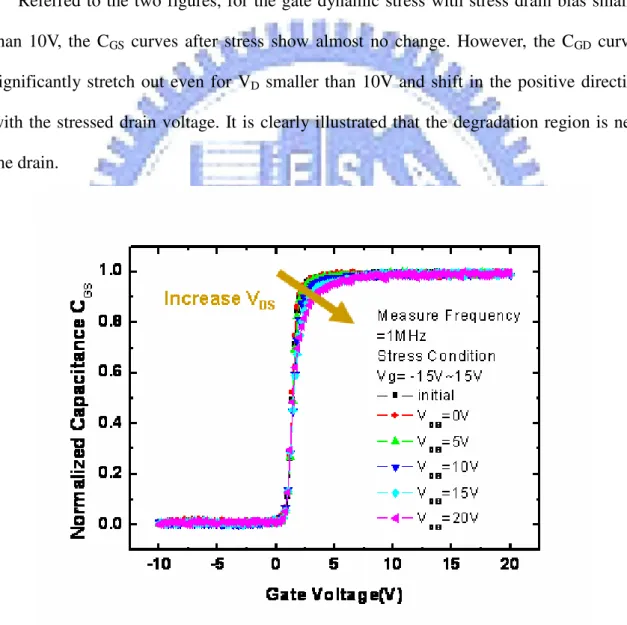
Since the Id-Vg transfer characteristics could not distinguish the dominant degradation region, C-V curves were therefore employed. Fig. 4-6(a) shows the normalized gate-to-source capacitance (CGS) curves before and after stress with different drain voltage.
Fig. 4-6(b) shows the normalized gate-to-drain capacitance (CGD) curves under the same
stress conditions. The CGS is measured with a floating drain and CGD is measured with a
floating source.
Referred to the two figures, for the gate dynamic stress with stress drain bias smaller than 10V, the CGS curves after stress show almost no change. However, the CGD curves
significantly stretch out even for VD smaller than 10V and shift in the positive direction
with the stressed drain voltage. It is clearly illustrated that the degradation region is near the drain.
Fig. 4-6(a) Degradation of normalized CGS curve in N-channel under various VDS in
Fig. 4-6(b) Degradation of normalized CGD curve in N-channel under various VDS in
on/off region at frequency=1MHz
4.2.2 Vg in the OFF region
Fig. 4-7 TFT model in N-channel under various drain bias in off region
Fig. 4-7 shows the arrangement N-type poly-Si TFT under various drain bias stressed in the off region. The gate signal frequency is also equal to 500KHz. Fig. 4-8(a) shows the I-Vg transfer curves of the TFT before and after 60s of dynamic gate stresses with
different drain voltage VDS. The higher threshold voltage, lower mobility and higher
sub-threshold swing are observed after stress just as the case discussed in section 4.2.1. The phenomenon of degradation under various VDS is similar to effects of hot carrier, too.
The initial mobility is 65 cm2/V-sec. It decreases to only 5 cm2/V-sec after AC stress with drain bias of 20 V. The initial sub-threshold swing is 0.26 V/dec. After the AC stress it degrades to 0.57 V/dec. They seriously depend on the supplied drain bias, as shown in Fig. 4-8(b) and Fig. 4-8(c). The degree of mobility degradation is the same in forward and reverse measurement, but the sub-threshold swing of reverse of VD=20V degrades more
than that in the forward measurement.
Fig. 4-8(a) Id-Vg forward curves before and after dynamic gate stress with various drain bias in off region
0 5 10 15 20 0.0 0.2 0.4 0.6 0.8 1.0
u
/u
0
V
DS(V)
Stress Condition Vg=0V~ -15V Tr=Tf=100ns Forward connection Reverse connectionFig. 4-8(b) Dependence of the mobility on VDS with gate AC stress in off region
0 5 10 15 20 0.2 0.3 0.4 0.5 0.6 0.7 0.8 0.9