有機雙穩態記憶體之製作與特性分析
66
0
0
全文
(2) 有機雙穩態記憶體 之製作與特性分析. 研 究 生:陳思元 指導老師:李柏璁. 教授. 國立交通大學光電工程系顯示科技研究所碩士班. 摘要 在本篇論文當中,我們成功製作出以有機材料為主的雙穩態記憶體元件。主要的結 構類似三明治架構,在兩個金屬電極中,嵌入一層有機半導體層。此結構在低電壓驅動 下,它處在高電阻狀態,也就是低導電性狀態;當持續增加電壓大於臨界電壓時,電流 會大幅提升而進入高導電性狀態。因此,此元件擁有兩種狀態,而我們定義它為”0” 和”1”。此元件之物理機制我們推測是藉由上電極與有機材料的蕭基接面及界面陷阱所 造成的。. 在之後的篇章中,我們又更進一步的簡化我們的元件結構,省去下電極的製程,而 形成 N 型參雜基板/有機材料/鋁的簡單結構。此元件的製程,只需要簡單的兩道蒸鍍製 程,大幅減去製程時間。另一方面,我們也探討有機材料的鍍率差異對元件電性的表現 有何影響,我們發現元件的臨界電壓會隨著有機材料的表面粗糙度愈大而變大,同時, 此結構在基板與有機材料之間有一極化現象,我們推測此現象會造成元件的臨界電壓變 大,以及造成元件的穩定度較差。. ii.
(3) Fabrication and Characteristics of Organic Bistable Memory Device Student:Szu-Yuan Chen Advisor:Prof. Po-Tsung Lee. National Chiao Tung University Department of Photonics & Display Institute. Abstract We have fabricated an electrical bistable device with a simple structure, an organic layer interposed between the Al electrodes. A bistable device is an electronic device with two conductivities at the same applied voltage. That is, at writing bias scan, the device holds at high resistance state at the beginning. It will switch into high conductance state as the sweeping voltage pass threshold voltage. After applying reading bias, the device still holds at high conductance state. Therefore, this device exhibits two distinctly different currents at the same applied voltage. The formation of the bistable states is probably caused by electron trapping by the defects at the Schottky junction under electrical field stressing. Later, we investigate another bistable device with Al/Alq3/n-type Si structure. It contains a heterostructure, and only two-layer deposition is needed in this structure. Current-voltage characteristic is similar to that of metal/organic semiconductor/metal structure, the three-layer structure widely used for organic memory devices, is obtained. Moreover, we are able to modify the electrical properties by utilizing appropriate deposition rates and thickness. This device shows extremely simple fabrication process and great potential in future advanced organic flexible display.. iii.
(4) Acknowledgements 首先我必須非常感謝養育我並且在求學期間一路支持我的家人,能讓我在這段路程 中能過著衣食無缺的生活,使我能專心於學業及其他各方面的發展。還有在這段期間一 直陪伴著我的前女友 vivien,她總是會在我遇到挫折與失落的時候給我最大的鼓勵及信 心,也會在成功的時候與我分享勝利的果實,非常感激她對我的支持。另外還有一路走 來的好夥伴好朋友,威成、高賽、安琪、郁盈、孟勳、楊偉、他米、家麒….等。從大學 以來,在彼此勉勵下,才能順利完成碩士班兩年學業。在這兩年裡,可以說是我人生當 中成長與改變最多的一個階段。在求學方面,從以往中制式的學習轉變成實際的操作, 許多的問題都大部分要靠自己去發掘或解決。因此在一個團體群的合作與互助也比以往 更顯得重要,另外在心態方面,也較為成熟,不再像大學時期嬉嬉鬧鬧。而以下是要感 謝這段時間當中幫助過我完成這篇文章的伙伴們。. 一開始要感謝我的指導教授李柏璁老師,謝謝老師在這兩年的蹲蹲教誨讓我受益良 多,也協助我渡過許多困難。另外,有許許多多幫助過我的學長和同學們,讓我在實驗 中遇到的困難能迎刃而解,在此都要非常感謝他們。特別是博士班學長張資岳,提供給 我了很多想法並且幫我解決許多疑惑,指導我們許多觀念上的問題。另外還有朝夕相處 的實驗室學長及同學們,盧贊文、江俊德、游嘉銘、曾仲銓、陳佳禾,還有因製程而互 相切磋學習的其他實驗室同學,謝謝他們的陪伴讓乏味的實驗室增添了許多色彩。最 後,也要謝謝最後這一年經常被我抓去做實驗的王明璽,多虧了他才能讓實驗迅速完 成,減輕我的負擔。. 最後要感謝經濟部學界科專的計畫補助,使得我們有足夠的資源能進行所有的研 究。再次感謝以上所有的人,豐富我在交大的兩年生活,並且協助我完成這份畢業論文。. 2007/6/22 于新竹 國立交通大學 交映樓 501 室. iv.
(5) Content Abstract (In Chinese)……………………………………………………………ii Abstract (In English)……………………………………………………………iii Acknowledgements……………………………………………………………..iv Content…………………………………………………………………………..v List of Tables……………………………………………………...……….….. vii List of Figures……………………………………………………………..…..viii. Chapter 1 1.1.. Introduction. Nonvolatile Memory…..……………………………………………….…1 1.1.1. Introduction...………………………………………………………1 1.1.2 Flash memory……...……………………………………………….3 1.1.3. Ferroelectric Random Access Memory…………………………….4 1.1.4. Magnetic Random Access Memory………………………………..6 1.1.5. Phase Change Random Access Memory…………………………..7. 1.2.. Organic Bistable Device…………………………………..……………...9. 1.3.. Summary and Outlook…………………………………………………..10. Chapter 2. 3-Layers Organic Bistable Memory Devices. 2.1. Introduction…………………………………………………..………......12 2.2. Fabrication of 3 Layers Organic Bistable Memory Device……….….......12 2.3. Electric Characteristic Measurement…………………………………..…16 2.4. Probable Conduction and Mechanism of Three Layer Device………..….19 2.5. Result and Conclusion.………………………………..……………….…31. v.
(6) Chapter 3. N-dope Si/Organic/Al Bistable Memory Device. 3.1. Introduction…………………………………………………….……….....32 3.2. Motivation…………………………………………...………………….....32 3.3. Fabrication of N-doped Si based Organic Bistable Memory Device……...33 3.4. Electric Characteristic Measurement………………………………………35 3.5. Investigation of Deposition Rate and Thickness in Organic Thin Film...…38 3.6. Difference in Erase Pulse of the N-dope Si Base Bistable Memory Device…………………………………………………………………...47 3.7. Conclusion…………………………………………………………….…...49. Chapter 4. Conclusion and Future Work. 4.1. Conclusion……………………………….………………..………….……51 4.2. Future Work………………………………………………………………..52. References………………………………………………………………….53 Vita……………………………………………………………………………56. vi.
(7) List of Tables Table1-1 Comparison of several non-volatile memory……...................................................2 Table2-1 The parameter of fabrication process……………………………………..……...16 Table3-1 The parameter of fabrication process…………………………………………….35 Table3-2 The important parameters of the devices with different deposition rates. (Vth: threshold voltage) ……………………………………………………………….39 Table3-3 The relative parameters of the reported organic bistable device……………..….49. vii.
(8) List of Figures Fig.1-1. (a) The structure of Flash memory. (b) The equivalent circuit of Flash memory. (c) The electron scheme of Flash in different state. (d) Description of. different Vth in. each states.…………………………………………………………………………..4 Fig.1-2. The principle instruction of FeRAM…………………………………………….…..5. Fig.1-3. The schematic cross section of MRAM………………………………………..……7. Fig.1-4. The basic structure of Phase-Change Random Access Memory……………….….. 8. Fig.1-5. The basic structure and Current-Voltage characteristic of organic bistable Memory…………………………………………………………………….………10. Fig.2-1. The chemical structure of Alq3 ………………………………………….……....13. Fig.2-2. The thermal deposition instrument………………………………………………....14. Fig.2-3. (a)The structure of 3 layer device.(b)The top view of the device……………….…14. Fig.2-4. I-V characteristics of Al/Alq3/Al (semi-log plot). Current is expressed in absolute value. A small jump in the off-current was observed on the way to the off/on transition around 2.3V……………………………………………………………...17. Fig.2-5. The ON/ OFF current ratio as a function of applied voltage………………….…...18. Fig.2-6. The Stability test on Al/Alq3/Al device in both ON and OFF states under applied voltage of t1V continuously. The retention time is over 1000sec.………………...19. Fig.2-7. The Current Density-Voltage characteristic in different device area……………....20. Fig.2-8 Typical current–voltage I–V curves with the structure ,Au(80 nm)/Alq3 (100nm)/Au(100 nm) ……………………………………………………….……..21 Fig.2-9. Schematic illustrations of the possible bistable behavior mechanism under several bias conditions.……………………………………………………………………..22. Fig.2-10. Typical current–voltage I–V curves with the structure (a) (■) Al(80 nm)/Alq3 (100nm)/Al(100 nm);. (b) (■) I–V curve for a Al(80 nm)/Alq3 (100nm) without. the top Al electrode and mechanically contacted with a small Al tablet (the off-current is lower because the contact area in that case is smaller than with the evaporated Al contact). No switching has been observed for applied bias up to 5 V.……………………………………………………………………………….....24 Fig.2-11. Schematic energy diagram of an Al/Alq3/Al structure. The lower energy barrier (Φ=1.28 eV) is between the work function of Al (5.8 eV) and the lowest unoccupied molecular orbital (LUMO) of Alq3. Therefore, the electron injection. viii.
(9) dominates the conduction process.…………………………………………….…25 Fig.2-12. Typical Capacitance–voltage C–V curves with the structure, Al(80 nm)/Alq3 (100nm)/Al(100 nm)……………………………………………………………...26. Fig.2-13. Experimental and slope fitted J/A**T2–E1/2 curves of the Al/Alq3/Al device in the OFF state at 0~0.7v. The slope of the curve is 0.00711. It is quite similar to the schottky model ideal value(0.007242)……………………………………...……28. Fig.2-14. Experimental and slope fitted J/E–E1/2 curves of the Al/Alq3/Al device in the OFF state 0.8~1.6v. The slope of the curve is 0.01322. It is quite similar to the schottky model ideal value(0.014485). ………………………………..….………….……29. Fig.2-15. Experimental and fitted J–V curves of the Al/Alq3/Al device in ON state with the Ohmic model. ………….…………………………………………………….……30. Fig.2-16 Experimental and fitted J–V curves of the Al/Alq3/Al device from OFF state to the ON state………….………………………………………………………...………36 Fig.3-1. Scheme of regular display panel structure…………………………………...…...33. Fig.3-2. (a) The structure of N-doped Si/Alq3/Al device. (b) The top view of the device….34. Fig.3-3. I-V characteristics of N-doped Si/Alq3/Al (semi-log plot). Current is expressed in absolute value. A small jump in the off-current was observed on the way to the off/on transition around 5.3V…………………….…………………………..…….36. Fig.3-4. The ON/ OFF current ratio as a function of applied voltage………………………37. Fig.3-5. The Stability test on Al/Alq3/Al device in both ON and OFF statesunder applied voltage of t1V continuously……………………………………………………….37. Fig.3-6. Current-voltage relations of organic dynamic random access bistable devices with different deposition rates. (-●-), (-●-), (-●-), (-●-), (-●-), and (-●-) represent writing cycle at low deposition rate(0.5A/s), reading cycle at low deposition rate(0.5A/s), writing cycle at middle deposition rate(1.5A/s), reading cycle at middle deposition rate(1.5A/s), writing cycle at high deposition rate(2A/s), and reading cycle at high deposition rate(2A/s), respectively……………………………………………..….39. Fig.3-7. Threshold Voltage-Deposition Rate relations of the organic bistable device…......40. Fig.3-8. Current-Deposition Rate relations of the organic bistable device. (-●-) and (-●-) represent low conductance state and high conductance state respectively. A small reading bias. of 1 V was applied to the device to detect the on or off state. current…………………………………………………...…………………………41 Fig.3-9. On/Off Current Ratio-Deposition Rate relations of the organic bistable device………………………………………………………………………………42 ix.
(10) Fig.3-10. Threshold Voltage-Alq3 film thickness relations of the organic bistable device. The organic film was deposited at 0.2nm/s. ………………………………………43. Fig.3-11. Current-organic film thickness of the organic bistable device. (-●-) and (-●-) represent low conductance state and high conductance state respectively. A small reading bias. of 1 V was applied to the device to detect the on or off state. current. ………………………………………………………………………….…43 Fig.3-12. On/Off Current ratio of the organic bistable device. The organic film was deposited at 0.2nm/s. A small reading bias of 1 V was applied to the device to detect the on and off state current. …………………………………..………….…44. Fig.3-13. linear-scale current-voltage characteristics of our bistable device deposited at 0.05nm/s. (-■-) and (-●-) represent writing cycle and reading cycle, respectively. ………………………………………..…….………………………..45. Fig.3-14. Band diagram of the proposed structure………………………………..…….…..45. Fig.3-15. The Alq3 surface morphology at 0.5A/s deposition rate. Mean roughness is 0.387nm. ………………………………………..…………....…………………….46. Fig.3-16. The Alq3 surface morphology at 1A/s deposition rate. Mean roughness is 0.351nm. ……………………………..…….…………………..…….…………….46. Fig.3-17. The Alq3 surface morphology at 2A/s deposition rate. Mean roughness is 0.312nm. ……………………………..…….……………..…….………………….47. Fig.3-18. Current-voltage relations of our organic bistable device. (-■-), (-●-), and (-▲-) represent writing and reading cycles after applying first, second, and third negative voltage pulses, respectively. ..…….………………………………….…...….……49. x.
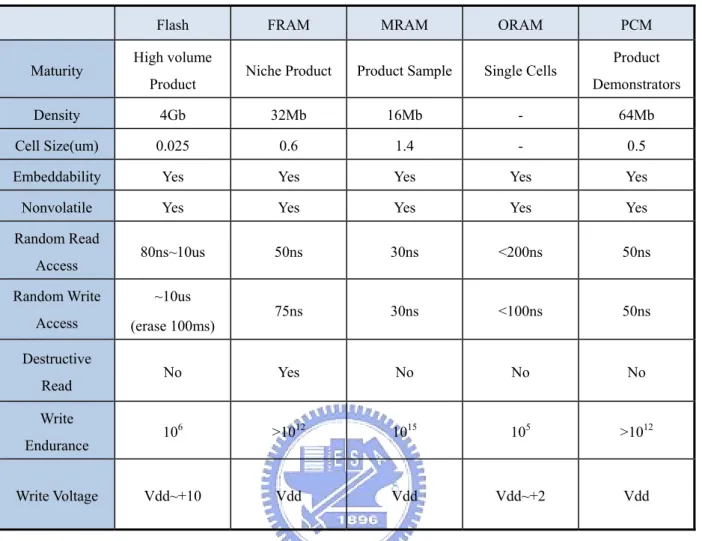
(11) Chapter 1. Introduction. 1.1. Introduction 1.1.1. Nonvolatile memory Recently, science has improved our life substantially. And the tech products are no longer just used for simple calculation, but they have also become requirements in our recreation life. Semiconductor memory devices have been investigated in the last fifty years. According to the devices which can maintain the data or not after turning off the power, we can divide them into two parts: volatile and non-volatile memory. In volatile memories operation, data information will not maintain in the device after turn off the power. The familiar volatile memories are DRAM (dynamic random access memory) and SRAM (static random access memory). In the other hand, the common non-volatile memories can keep up the data permanently, but the storage speed is much slower than the dynamic random access memory or cache memory. So, the computer systems always demand both of them to store the information in the same time. Most of personal digital products (such as mobile phone, personal digital assistant, digital camera, and MP3 player, etc.) already use non-volatile memories, it is because that the non-volatile memories have many advantages, such as small size, faster access time, low power consumption, and so on. For the time being, flash memory is the most popular non-volatile memory in the application products. It is based on silicon material. It can be well versed manufactured largely and high yield. But, low writing speed and high power consumption are both its drawbacks. In order to overcome these problems, many researchers have developed four new type non-volatile memories; there are FeRAM, MRAM, OUM, and OBD.. And I’ll give. some short introduction about each of them later. The comparison of several 1 .
(12) non-volatile memories is shown in table1.1. Flash Maturity. High volume Product. FRAM. MRAM. ORAM. Niche Product. Product Sample. Single Cells. PCM Product Demonstrators. Density. 4Gb. 32Mb. 16Mb. -. 64Mb. Cell Size(um). 0.025. 0.6. 1.4. -. 0.5. Embeddability. Yes. Yes. Yes. Yes. Yes. Nonvolatile. Yes. Yes. Yes. Yes. Yes. 80ns~10us. 50ns. 30ns. <200ns. 50ns. 75ns. 30ns. <100ns. 50ns. No. Yes. No. No. No. 106. >1012. 1015. 105. >1012. Vdd~+10. Vdd. Vdd. Vdd~+2. Vdd. Random Read Access Random Write. ~10us. Access. (erase 100ms). Destructive Read Write Endurance Write Voltage. Table 1.1: Comparison of several non-volatile memories.. 2 .
(13) 1.1.2. Flash memory Flash memory [1]-[8] is the most popular memory device nowadays. The structure of flash memory is similar to MOSFET, as shown in figure 1-1. But the difference between both devices is floating gate. Flash memory uses floating gate to storage charge. The material of floating gate is poly silicon, which is covered by insulator. So the stored charge can’t be released without any bias. Therefore, the data can be stored in the flash memory when power turning off. The “1” and “0” are represented the charge in the floating gate or not. When the state of the device is “0”, we can program data into it. We apply high voltage between gate and base electrode so that the mobile electron in the channel can be tunneled into floating gate due to the high electric field. In other aspect, if we want to read the data of device, we just apply a constant voltage in the range of the preprogrammed and programmed threshold voltage on gate electrode and measure the current between drain and source electrode. When there are some electrons in the floating gate, the Vth is bigger than reading voltage. So we can’t measure any drain current, and we define the state is logic 1( or 0). In other word, if there are no electrons in the floating gate, the Vth of the device is smaller than the reading voltage. Hence, we can detect drain current, and define the state is logic 0 (or 1). Therefore, we can measure the different drain current to determine that the charge in the floating gate or not. Due to the tunneling effect in programmed process, the operation speed and rewritable times should be confined. As rewrite many times, insulator might break down. Hence, flash generally can be rewritten about 106 times.. 3 .
(14) Gate . Metal Oxide . polysilicon . Source . Drain . Drain Gate . N . tunnel . N Floating Gate . Substrate(P‐Si) . Source . Fig.1-1: (a) The structure of Flash memory. (b) The equivalent circuit of Flash memory.. 1.1.3.. FeRAM ( Ferroelectric Random Access Memory). In order to improve the drawbacks of Flash memory (such as high program and erase voltages, slow program speed, write-erase endurance that is limited to ~105 cycles), researchers are looking new generated memories which have fast speed, low power consumption. Among all new memories, ferroelectric random access memory (FeRAM). [9]-[13]. is the first device for application in our life. But it has a significant. problems for us to overcome, that is fewer reading times. M.Lim had reported that present FeRAM just can be read about 1012 times, and due to this drawback, FeRAM is hard to apply for our life. The structure of ferroelectric RAM is similar to DRAM. The mechanism of FeRAM is dominated by the location of the free atoms in ferro-crystal materials, such as figure 1-2. Many people have hoped that FeRAM will be the best memory in our 4 .
(15) future life, because it has several advantages, such as SRAM, DRAM and Flash. In operation, FeRAM is similar to DRAM. Writing is accomplished by applying a field across the ferroelectric layer by charging the plates on either side of it, forcing the inner atoms "up" or "down" (depending on the polarity of the charge), thereby storing a "1" or "0". In reading process, however, is somewhat different than in DRAM. The transistor forces the cell into a particular state, say "0". If the cell already held a "0", nothing will happen in the output lines. If the cell held a "1", the re-orientation of the atoms in the film will cause a brief pulse of current in the output as they push electrons out of the metal on the "down" side. The presence of this pulse means the cell held a "1". Since this process overwrites the cell, reading FeRAM is a destructive process, and requires the cell to be re-written if it was changed.. Fig.1-2: The principle instruction of FeRAM. Generally the operation of FeRAM is similar to ferrite core memory, one of the primary forms of computer memory in the 1960s. In comparison, FeRAM requires far less power to flip the state of the polarity, and does so much faster. The requirement for a write cycle for each read cycle, together with the high but not infinite write cycle limit, poses a potential problem for some special applications 5 .
(16) 1.1.4.. MRAM (Magnetic Random Access Memory). Magnetoresistive Random Access Memory (MRAM) [14]-[18] is also a non-volatile computer memory technology, which has been under development since the 1990s. Continued increases in density of existing memory technologies, but its proponents believe that the advantages are so overwhelming that MRAM will eventually become dominant. Unlike conventional RAM chip technologies, in MRAM data is not stored as electric charge or current flows, but by magnetic storage elements, as shown in figure 1-3. The elements are formed from two ferromagnetic plates, each of which can hold a magnetic field, separated by a thin insulating layer. One of the two plates is a permanent magnet set to a particular polarity, the other's field will change to match that of an external field. A memory device is built from a grid of such "cells". Reading is accomplished by measuring the electrical resistance of the cell. A particular cell is selected by powering an associated transistor, which switches current from a supply line through the cell to ground. Due to the magnetic tunnel effect, the electrical resistance of the cell changes due to the orientation of the fields in the two plates. By measuring the resulting current, the resistance inside any particular cell can be determined, and from this the polarity of the writable plate. Typically if the two plates have the same polarity this is considered to mean "0", while if the two plates are of opposite polarity the resistance will be higher and this means "1". Data is written to the cells using a variety of means. In the simplest, each cell lies between a pair of write lines arranged at right angles to each other, above and below the cell. When current is passed through them, an induced magnetic field is created at the junction, which the writable plate picks up. This pattern of operation is similar to core memory, a system commonly used in the 1960s. This approach requires a fairly 6 .
(17) substantial current to generate the field, however, which makes it less interesting for low-power uses, one of MRAM's primary disadvantages.. Magnetic Memory Cell Size <1um H. Wire Line. Current. Wire Line. Fig.1-3: The schematic cross section of MRAM Furthermore, MRAM has infinity write-read-erase cycle times, this is the best advantage of all nonvolatile memory. But the high current consumption is the most problem for MRAM in the present. So it should be improved better in the future.. 1.1.5.. PRAM (Phase Change Random Access Memory). Phase-change memory (also known as PCM, PRAM, Ovonic Unified Memory) [18]-[26]. is another type of non-volatile computer memory. PRAM uses the unique. behavior of chalcogenide glass, which can be "switched" between two states, crystalline and amorphous, with the application of heat, as shown in figure 1-4.. PRAM is one of a number of new memory technologies that are attempting to compete in the non-volatile role with the almost universal Flash memory, which has a number of practical problems these replacements hope to address. The crystalline and amorphous states of chalcogenide glass have dramatically 7 .
(18) different electrical resistivity values, and this forms the basis by which data are stored. The amorphic, high resistance state is used to represent a binary 0, and the crystalline, low resistance state represents a 1. Chalcogenide is the same material utilized in re-writable optical media (such as CD-RW and DVD-RW). In those instances, the material's optical properties are manipulated, rather than its electrical resistivity, as chalcogenide's refractive index also changes with the state of the material. Although PRAM has not yet reached the commercialization stage for consumer electronic devices, nearly all prototype devices make use of a chalcogenide alloy of germanium, antimony and tellurium (GeSbTe) called GST. It is heated to a high temperature (over 600°C), at which point the chalcogenide becomes a liquid. Once cooled, it is frozen into an amorphic glass-like state and its electrical resistance is high. By heating the chalcogenide to a temperature above its crystallization point, but below the melting point, it will transform into a crystalline state with a much lower resistance. This phase transition process can be completed in as quickly as five nanoseconds, according to a January 2006 Samsung Electronics patent application concerning the technology. This is comparable to conventional memory devices, for instance, modern DRAM cells have a switching time on the order of two nanoseconds. Polycrystalline Chalcogenide. Metal Interconnect. Programmable Volume Conductive Resistive. Bit. Resistive Heater n P+ . Word. Fig.1-4: The basic structure of Phase-Change Random Access Memory 8 .
(19) 1.2. OBD (Organic Bistable Device) The first organic bistable device was issued in the organic photoelectric research laboratory of UCLA in 2002 Component. [27]-[29]. , as shown in Fig. 1-6. The organic. semiconductor material is not only developed to some extent in the photoelectric field but also in semiconductor Field. The UCLA organic photoelectric research laboratory issued organic memory device that uses the organic layer, AIDCN (2- amino-4,5 imidazoledicarbonitrile), it is the single crystal structure, as shown in Fig. 1-6 (c). The structure of organic bistable device is five layers. (Fig.1-6 (b)), its component structures have two metal electrode inserted for "organic layer / intermediate level /organic layer " sandwich structure. Applying a bias through the electrodes, as the bias has not reached the threshold voltage, the current is quite small, about 10-8 amperes. And it defines to be 0 state at this moment; When the bias voltage is reaching the threshold voltage, the electric current will suddenly rise to 10-2 amperes, and it will be defined as the state 1 (Fig. 1-6 (a). This is two kinds of states of the organic bistable device: High conductive rate (1) and the state of low conductive rate (0 ), the difference in electric conduction is up to 106. And it needs about 10ns to change the high electric conduction into the low electric conduction state. It is to say that writing time needs 10ns. After reaching the state of the high conductive, turn off the power, the device is still at the high conductive state, therefore it has function of storing data. If we want to erase the data, that is to say that makes the component reply into a low conductive state, it should apply a reverse voltage to return to the low conductive rate state. The mechanisms of two kinds of states have not had a suitable theory yet at present to prove.. 9 .
(20) Fig.1-5: The basic structure and Current-Voltage characteristic of organic bistable Memory . 1.3. Summary And Outlook Electrically addressable bistable devices based on organic films have been developed for memory applications. Several materials and device structures with bistable states have been reviewed, including the organic/metal-nanocluster/organic structure, polymer composites blended with synthesized metal NPs, polymer nanofibers decorated with NPs, and donor–acceptor complexes. I–V characteristics show a conductance change of at least three orders of magnitude. These transitions between the ON and OFF states can be triggered on a nanosecond time scale. The fast response times suggest that the switching is due to electric-field-induced charge transfer. The bistable effect is a fascinating phenomenon covering physics, chemistry, and materials science. The abrupt transition of electrical conductivity on a nanosecond time scale is a quantum phenomenon, although observed in a large-scale device. Although these devices show promising performance, they are still in the early stages of research. Several important issues are still not clear at this moment. For example, what are the device mechanisms and what is the ultimate in device performance? These questions are not only important for satisfying scientific interests, but are also 10 .
(21) important for future practical applications. By resolving these scientific issues, we believe that much more interesting phenomena will be discovered and these organic bistable devices will open a new direction for future organic electronics. In this thesis, we will use OLED material, Alq3 to demonstrate a single layer organic bistable device. The structure is the same as the paper that have delivered before. And we try to find out the mechanism of our devices. On the other hand, we also try to speculate the probable mechanism of the memory device. More important, we try to save our fabrication time by reducing our device structure. Finally, we want to integrate the organic bistable device into OLED in the future. 11 .
(22) Chapter 2. 3-Layer Organic Bistable Memory Devices. 2.1.. Introduction The device with a single-layer structure sandwiched between two metal. electrodes is introduced in this section. The chemical structure of the material is presented in the following. The material layers of these devices are deposited by thermal evaporation, so it is imperative that this process is accurately controlled in order to generate functional devices. The I-V characteristic and the probable mechanism in this structure will be presented, too. Besides, the modified fabrication processes and structures will be introduced in later chapter.. 2.2.. Fabrication of 3 Layer Organic Bistable Memory Device. In the organic bistable device, the organic layer is playing a very important role. Therefore, in the experiment, the purity and the quality of the material should be considerated well. The materials used in this experiment are as follows: The organic layer is Tris(8-hydroxyquinoline) aluminum (Alq3), which is one of the well-known organic electron transfer semiconductor materials, as shown in Fig. 2-1. Alq3 is made and purified by the Seachent CO. LTD, and the purity is 95%. The metal electrode are aluminium (Al ) and gold(Au), they are produced by Sumitomo and Tanaka Company, respectively, and the purity are of both up to 99.999%.. 12 .
(23) Fig.2-1: The chemical structure of Alq3.. Many organic materials are deposited by the thermal evaporation at present. Using thermal evaporation to deposit organic thin film has the following advantages: first of all, heated by the resistance wire, so the temperature can be perfectly controlled; in addition, the material is heated in the wide area, hence it could be heated uniformly without overheating problem. Moreover, it can heat many boat at the same time, so we can co-evaporate different material together; finally, the structure of thermal coater is very simple and the cost could be dropped down. Therefore, I’ll use thermal coater to deposit the thin film in my research and use metal hard mask to define the pattern of the device. There are five tungsten boats to heat the material and two quartz oscillators to record the thickness of the thin film. Before depositing the thin film, it should pump out the air lower than 7.56x10⁻²torr by the machine pump. And then use cryo-pump to drop down the vacuum lower than 3x10⁻⁶torr. Afterward, begin to heat the boat to fabricate the membrane. The thermal deposition instrument is shown in figure2-2.. 13 .
(24) Fig.2-2: The thermal deposition instrument. In the experiment, there are three layers in the organic bistable device. The device is based on silicon substrate with wet oxide, as shown in Fig.2-3(a). The organic material is sandwiched between two metal electrodes. During the thermal evaporation procedure, the shadow mask was used to pattern and define the electrode area. The top and bottom Al electrode were thermally evaporated with linewidth of 800 μm through a shadow mask. The top and bottom electrodes were aligned perpendicular to each other, so as to define an active cross area of 800 × 800 μm, as shown in Fig.2-3(b).. Al Alq3 Al Wet Oxide Silicon Substrate Fig.2-3: (a) The structure of 3 layer device.. 14 .
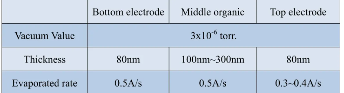
(25) Fig.2-3: (b) The top view of the device. During the evaporation procedure, any pollutant or dust will destroy the device’s performance and yield. Hence, the substrate surface which is clean or not will plays an important role. The washing step of the substrate is as follows: first of all, dip in the DI water about 5 minutes; second, immerse in the H2SO4:H2O2 about 10 minutes at 75~85oC to decompose the oxidation, then dip into diluted HF to remove chemical oxide. Afterward, use diluted NH4OH and HCl to remove little particle and alkaline metal; later, dip into diluted HF again to remove chemical oxide. Finally, I use N2 to blow the water away and prepare to deposit the film later. The active layer of the organic bistable device (OBD) consists of a nominal organic single layer structure interposed between an anode and a cathode, as shown in the Figure 2-3(a). The device is implemented with a metal–insulator–metal (MIM) structure that was fabricated through the following process: first of all, the thermal oxide is deposited by oxidation and diffusion furnaces systems. Then, the 80nm Al bottom electrodes were thermally evaporated on it through a shadow mask at a pressure of approximately 3x10⁻⁶ Torr. Then, an Alq3 film was deposited on top of 15 .
(26) the electrodes by thermal vapor deposition. The thickness of this organic layer is 100 nm. Finally, the top 80nm Al electrode was deposited by thermal evaporation at a pressure of 3 × 10⁻⁶ torr through a shadow mask. Every fabrication parameter is shown in Table 2-1.. Bottom electrode. Middle organic. Top electrode. 3x10⁻⁶ torr.. Vacuum Value Thickness. 80nm. 100nm~300nm. 80nm. Evaporated rate. 0.5A/s. 0.5A/s. 0.3~0.4A/s. Table 2-1: The parameter of fabrication process. 2.3.. Electric Characteristic Measurement Current-voltage (I-V) characteristics were measured with a HP 4156B, where. voltage was changed at stepping rate of 0.1 V/sec. A typical current–voltage (I–V) curve for an OBD is shown in Figure 2-4. It distinctively displays two conducting states. With an applied voltage on the as-fabricated device, although the current increases slowly with the voltage, the current remains low. The current is in the range of 10−9 A at 1 V. This is the low conductivity state ( we define it as “OFF” state). When the applied voltage is increased further to ~2.3 V, a sharp increase in the current is observed, indicating the device transition from the OFF-state to a high conductivity state (we define it as “ON “state). This transition from the OFF-state to the ON-state serves as the “writing” process for the memory device. For the programmed device, the device shows a higher current as the voltage apply. The current density at 1 V is about 10−2 A/cm2. This current is seven orders of magnitude higher than that in the OFF state. Curve b in Fig. 2-4 shows a sweep from 0 to 3 V 16 .
(27) after the first sweep. It can be seen that the device, after reaching its high conductivity. Current(A). state, remains in this ON-state although the power is off.. 0.1 0.01 1E-3 1E-4 1E-5 1E-6 1E-7 1E-8 1E-9 1E-10 1E-11 1E-12 0.0. Curve b . Curve a . 0.5. 1.0. 1.5. 2.0. 2.5. 3.0. Voltage(V) Fig.2-4:. I-V characteristics of Al/Alq3/Al (semi-log plot). Current is expressed in. absolute value. A small jump in the off-current was observed on the way to the off/on transition around 2.3V .. The Figure2-5 shows the ratio of the ON-state to the OFF-state current as a function of the applied voltage. The distinct bi-electrical states in the voltage ranging from 0 to 2.3 V allow a low voltage (e.g., 1.0 V) to read the “0” or “OFF” signal (before writing) and “1” or “ON” (after writing) signal of the device. Therefore, the on/off ratio of our device is big enough to avoid the judgment error. 17 .
(28) 8. 10. 7. 10. 6. On/Off Ratio. 10. 5. 10. 4. 10. 3. 10. 2. 10. 1. 10. On/Off Ratio. 0. 10. -1. 10. 0.0. 0.5. 1.0. 1.5. 2.0. 2.5. 3.0. Voltage(V) Fig.2-5: The ON/ OFF current ratio as a function of applied voltage. At the same time, the memory retention ability of these devices under a bias stress was evaluated by leaving the devices in the ON state and OFF state at ambient conditions and measuring the current in a continuous as shown in Fig.2-6. The voltage (~1V) is applied in the ON and OFF states and the current was read at 60 s intervals. It is found that no detectable degradation of the ON and OFF states is observed at least over 1000 second, The result of the stress test indicates that the OFF and ON states are not transient states.. 18 .
(29) 1E-3 1E-4. Current(A). 1E-5 1E-6. On State Off State. 1E-7 1E-8 1E-9 1E-10 1E-11. 0. 200. 400. 600. 800. 1000. 1200. Time(s). Fig.2-6: The Stability test on Al/Alq3/Al device in both ON and OFF states under applied voltage of +1V continuously. The retention time is over 1000sec.. 2.4.. Probable Conduction and Mechanism of Three Layer Device The structure of the Al/Alq3/Al device corresponds well with the report of. Chia-Hsun Tu group’s, but the differences are the fabrication method and the bistable behavior. In Tu’s Device[44], they deposited the organic active layer, Alq3 by spin coating. Alq3 was dissolved in 1,2-dichloroethane solvent with a magnetic stirrer at room temperature. And the solution was then spin coated on the Al/Si substrate. After spin coating, the films were baked at 100◦C for 2 min and vacuumed at 1 × 10⁻⁵ torr for 1 hour. The fabrication of electrodes were the same as ours method, thermal evaporation. In the I-V characteristic, the switch-on and switch-off process can be achieved in the same sweeping direction in Tu’s device. It is the most difference between our deivces. Although our device structure is the same as the Tu’s device, but we assume that the origin of the bistable behavior is different. Tu’s group suggested that the switching phenomenon of the memory device is explained on the basis of filament theory. But we suggest that the mechanism is dominated by the interface traps. During the top metal deposition, the interface where they can aggregate to form 19 .
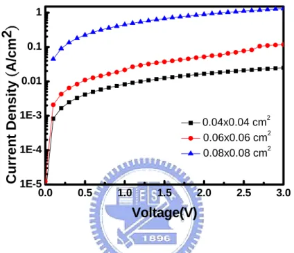
(30) traps, and it was shown that such trap form phenomenon increases when decreasing the deposition rate in organic deposition process, we will discuss in later chapter. Here, we first propose that current density is dependent on the device area; as shown in the Fig. 2-7.. Current Density (A/cm2). 1 0.1 0.01 1E-3. 2. 0.04x0.04 cm 2 0.06x0.06 cm 2 0.08x0.08 cm. 1E-4 1E-5 0.0. 0.5. 1.0. 1.5. 2.0. 2.5. 3.0. Voltage(V) Fig. 2-7: The Current Density-Voltage characteristic in different device area.. In Figure 2-7 shows the typical current–voltage I–V characteristics of three different area devices. Each device exhibit the same kind of bistable behavior, they turn into a highly conductive state, the on-state, above a certain threshold voltage, but they have different on state, the bigger size area device has higher current density, in contrast to the bigger device has smaller current density. It implies that the current density is dependent on the device’s size. Hence we can eliminate the filament effect from the mechanism of switching phenomenon. This is because that the current flows through the device should be equaled in unit area if it were dominated by the filament conducting effect. 20 .
(31) In another aspect, Ajit Kumar Mahapatro[45] have also reported an electric-field-induced conductance transition from an insulating state to a conducting state in a thin layer of Alq3 sandwiched between two metal electrodes. The switching behavior is absent in devices in which both electrodes have a high work function, indicating that efficient electron injection has an important role in the electric-field-induced switching behavior of Alq3-based single-layer devices. Its mechanism is due to the different Alq3 molecular phase. Alq3 has an octahedral symmetry and occurs in two geometrical isomers: meridian (mer-Alq3) and facial (fac-Alq3), which is more insulating then mer-Alq3 due to larger HOMO-LUMO gap. When the device is at the off state, Alq3 is in facial geometrical isomer, when the device is at the on state, Alq3 is in the meridian geometrical isomer. But, we want to demonstrate that the bistable effect is independent of the Alq3 molecular geometric structure. Therefore, we also fabricate the 3layer memory device, but the gold is used as electrodes here. This device shows the bistable characteristics, too. It is quite different from the device, Au/Alq3/Au which delivered by Ajit Kumar Mahapatro. Hence, the mechanism of our device may be not dominated by molecular geometrical ifferent proposed by Ajit Kumar Mahapatro. The I-V characteristic of our device is shown in the Fig2-8. 0.1 0.01 1E-3. Current(A). 1E-4 1E-5 1E-6 1E-7 1E-8. Au/Alq3/Au. 1E-9. 8mmx8mm. 1E-10 0. 1. 2. 3. 4. 5. Voltage(V). Fig.2-8: Typical current–voltage I–V curves with the structure ,Au(80 nm)/Alq3 (100nm)/Au(100 nm); 21 .
(32) (a). (b). (c) Figure 2-9: Schematic illustrations of the possible bistable behavior mechanism under several bias conditions.. Figure 2-9 shows the schematic illustrations of the possible bistable behavior mechanism under the bias conditions. We assume that the initial state is the OFF state. This means that trapping sites near the top Al/organic interfaces are uncharged. When 22 .
(33) applied low bias (~0V to 0.7V), due to the traps at the top Al/Alq3, the carrier will be caught by those traps, and there is small current flow in the OFF state by Schottky emission. When the voltage was ramped from 0.7V to 1.4V, due to captured charges at the interface, they would bend the band of Alq3, and the carriers would be transferred through the traps to the opposite electrode; in the contrast, When the voltage was ramped up to +2.3V (above the threshold voltage), due to captured charges at the interface, it would decrease the barrier between Al/Alq3 and induce the tunneling current through the organic film to the opposite electrode, hence the current has a sharp increase and the device has had a transition from the high impedance state to a low-impedance state. In order to prove our suggestion, the bistable effect in the device is attributed to the inclusion of traps at the Al/Alq3 interface during the evaporation of the top electrode. The proof is that we have not observed a bistable effect in our device if the Alq3 is directly and gently contacted by a mechanical contact ingot, as shown in Fig. 2-10.. 23 .
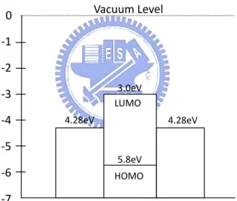
(34) (a) . (b) . 1E-8. C Current(A) t(A). 1E-9. (a) . 1E-10 1E-11. (b) . 1E-12 1E-13 0. 1. 2. 3. 4. 5. Volta age(v) Fig.2-10: Typical cuurrent–voltage I–V currves with thhe structuree (a) (■) Al(80 A Al(100 nm)); nm)/Alq3 (100nm)/A. (b) (■)) I–V curvve for a A Al(80 nm)/A Alq3. w the top Al electtrode and mechanically m y contacted with a smaall Al (100nm) without tablet (thee off-currennt is lower because thee contact arrea in that case is sm maller than with the evaporaated Al conttact). No sw witching hass been obserrved for app plied bias up to 5 V.. In Al/Alqq3/Al devicees, the schem matic energ gy diagram is shown inn Fig.2-11. The low wer energy barrier b (Φ=11.28 eV) is between b thee work funcction of Al ((5.8 eV) and d the low west unoccuupied moleecular orbittal (LUMO O) of Alq3, indicatingg that elecctron injeection from Al into the LUMO of Alq3 is thee favored prrocess. Holee injection from f 24 .
(35) Al (Φ=4.28 eV) into the highest occupied molecular orbital (HOMO) of Alq3 will be much more difficult because of the high energy barrier. Thus electron injection dominates the conduction process. To further prove that the bistable characteristic is dependent on the traps at the top Al and Alq3 interface. We demonstrate the capacitance characteristic as shown in Fig.2-12. When the applied voltage is increased further to Vth, a sharp decrease in the capacitance is observed, indicating the device transition from the OFF-state to a high conductivity state. At the same time, we can firmly believe that there are some traps at the interface or in the bulk.. Vacuum Level . 0 ‐1 ‐2 . 3.0eV LUMO . ‐3 ‐4 . 4.28eV . 4.28eV . ‐5 5.8eV . ‐6 . HOMO . ‐7 Fig. 2-11: Schematic energy diagram of an Al/Alq3/Al structure. The lower energy barrier (Φ=1.28 eV) is between the work function of Al (5.8 eV) and the lowest unoccupied molecular orbital (LUMO) of Alq3. Therefore, the electron injection dominates the conduction process.. 25 .
(36) 3.49E-011 3.49E-011 3.49E-011. 1E-6. 3.48E-011 1E-7. 3.48E-011. Capacitance(F). Current(A). 1E-5. 3.48E-011. 1E-8 0. 2. 4. Voltage(V) Fig.2-12: Typical Capacitance–voltage C–V curves with the structure, Al(80 nm)/Alq3 (100nm)/Al(100 nm);. On the other hand, to further understand the device transition from the OFF state to the ON state in bistable memory behavior, the J–V curves in both states were analyzed in terms of theoretical models. For the OFF-state from 0 to 0.7 volt, the J–V curve can be translated to lnJ/T2-E1/2 curve. Due to the same linear relationship between experiment date and the Schottky emission model, we can suggest that the current was controlled by charge injection from the electrode from 0 volt to 0.7 volt. The description and the figure are shown below:. 26 .
(37) ⎡ ⎛ qEi ⎢ −q ⎜ Φ B − 4πε i J = A **T 2 exp ⎢ ⎝ ⎢ kT ⎢ ⎣ − qΦ B J = + ln 2 A **T kT. qEi. 4πε i. kT. 1. E2. n = 1.73 ⇒ ε i = 1.732 × 8.85 × 10−14 F k = 8.62 × 10⁻⁵ eV. ⎞⎤ ⎟⎥ ⎠⎥ ⎥ ⎥ ⎦. cm. K. T = 300 K q ⇒ slope =. qEi. 4πε i. kT. = 0.007242. T is room temperature (298 K), Φ B is the barrier height, εi is the insulator permittivity We first transform the Schottky emission model equation into ln(J/T2) versus E1/2 form, and then calculate the slope of the curve. We can find that the experimental slope (0.00711) is quite equal to the ideal value (0.007242), as shown in figure2-13. Hence, we can infer that the off-state from 0~0.7v is controlled by the charge injection from the electrode. Due to the injection charge, the barrier may be decreased and bended.. 27 .
(38) -25. ln(J/A*T2). e. -26. e. -27. e. Experiment, 0~0.7V Schottky Fitting, Slope=0.00711. -28. e. 200. 300. 400. 500. 600. 700. 1/2. E. Fig.2-13. Experimental and slope fitted J/A**T2–E1/2 curves of the Al/Alq3/Al device in the OFF state. The slope of the curve is 0.00711. It is quite similar to the schottky model ideal value (0.007242).. Subsequently, we try to find out the current relationship from 0.8 volt to 1.6 volt in the off state, we first transform the Poole-Frenkel model equation into ln(J/E) versus E1/2 form, then calculate the slope of the curve. We can find that the experimental slope (0.01322) is quite equal to the ideal value (0.014485), as shown in Fig2-14. Hence, we can infer that the off-state from 0.8~1.6v is controlled by the traps at the interface between the electrode and the organic film. The description and the figure are shown below:. ⎡ −q(φB − qE πε i ) ⎤ J ∝ E exp ⎢ ⎥ kT ⎥⎦ ⎣⎢ ⎡ −qφB q πε i ) 12 ⎤ J + ln( ) ∝ ⎢ E ⎥ E kT ⎣⎢ kT ⎦⎥ q q πε i ) kT. = 0.014485 28 . .
(39) 4. ln(J/E). e. Experiment, 0.8~1.6V PF Fitting, Slope=0.01322 3. e 200. 220. 240. 260. 280. 300. 320. 1/2. E. Fig.2-14. Experimental and slope fitted J/E–E1/2 curves of the Al/Alq3/Al device in the OFF state at 0.8~1.6v. The slope of the curve is 0.01322. It is quite similar to the Poole Frenkel model ideal value (0.014485).. For the ON state, the J–V curve can be simulated by the Ohmic model as follows:. J. E exp. ∆E kT. Vexp. c kT. c is a positive constant independent of V or T. The J–V characteristic shown in Fig.2-15 suggests that, after the electrical transition, the current through the device changed from a charge injection current to a ohmic conduction current.. 29 .
(40) 1.4. Current Density(J). 1.2 1.0 0.8 0.6 Experiment. 0.4 0.2 0.0 0.0. 0.5. 1.0. 1.5. 2.0. 2.5. 3.0. Voltage(V) Fig.2-15. Experimental and fitted J–V curves of the Al/Alq3/Al device in ON state with the Ohmic model.. 0.01. Current(A). 1E-3 1E-4 1E-5 1E-6. Ohmic Fitting PF Fitting Schottky Fitting. 1E-7 1E-8 0.0. 0.5. 1.0. 1.5. 2.0. 2.5. 3.0. Voltage(V) Fig.2-16. Experimental and fitted J–V curves of the Al/Alq3/Al device from OFF state to the ON state.. 30 .
(41) 2.5.. Result and Conclusion. In this chapter, we have fabricated an electrical bistable device with a simple structure, that is, an organic layer interposed between the Al electrodes. Our device is the same as Tu’s device with a triple-layer structure. But the electrical bistable behavior is not the same. The electrical bistability was assumed to occur as a result of the interface trapped charges. And the key issues for the appearance of electrical bistability are pointed out. First of all, we propose that the bistable effect is independent of the filament effect and the molecular geometric structure; second, the top metal should be deposited through the thermal process, and the metals are not much related the effect; third, we measure the C-V curve of the device and we can sure the traps effect. Afterwards, we propose the probable mechanism model of the device. We believe this is one of the most clear-cut experimental data on the electrical bistability that is helpful for further understanding of the electrical bistable behaviors in organic thin film devices. Finally, we show that the current through the device changed from Schottky emission and Poole Frenkel emission to an ohmic conduction current.. 31 .
(42) Chapter 3. N-dope Si / organic / Al Bistable Memory Devices. 3.1.. Introduction Recently, several organic materials have been proposed for electronic and. opto-electronic devices, such as organic thin film transistors (OTFT), organic light emitting diodes (OLED), and solar cells, etc. Furthermore, several groups pay close attention to another important electronic application, organic bistable memory device [1-12]. Electrical bistable behavior is a phenomenon where a device exhibits two different conductivities at the same applied voltage. Due to this bistable behavior, organic bistable device is ideal for rewritable nonvolatile memory application. In this chapter, we fabricate and investigate organic memory devices with Al/ tri-(8–hydroxyquinoline)–aluminum (Alq3) deposited on n-type Si substrate. The formation of the bistable states is caused by electron trapping by the defects in the device under electrical field stressing and the surface polarization effect. This device exhibits two different conductive states at the same applied voltage and it is found to exhibit distinct bistability with an on/off current ratio up to 105. Furthermore, this device shows more than 1000s data retention time. Hence, we believe that these discoveries pave the way for next generation electrically addressable data storage devices.. 3.2.. Motivation Requirements for more accurate simulations in research and for media. entertainment of consumer electronics are increasing day by day. As a result, demand for the memory capacity is stepping up as well. Scaling of technology and changing 32 .
(43) storage media can make these possible. For some specific applications, e.g. displays, e-papers, and smart cards, potential memory devices based on polymeric or organic materials are always there. In this work, organic dynamic random access memory devices with Al/ tri-(8–hydroxyquinoline) -aluminum (Alq3) deposited on n-type Si substrate at different deposition rates for the organic layer are investigated for the future application in displays. Moreover, the electrical properties of the device can be controlled easily by tuning deposition rate.. Fig.3-1: Scheme of regular display panel structure. 3.3.. Fabrication of N-doped Si Base Bistable Memory Device In the experiment, there are only two layers in the organic bistable device. The. device is based on silicon substrate, as shown in Fig.3-3(a). The organic material is directly deposited on n-doped si substrate. During the thermal evaporation procedure, the shadow mask was used to pattern and define the electrode area. The top Al electrode were thermally evaporated with area of 800x800μm2 through a shadow mask, as shown in Fig.3-3(b).. 33 .
(44) Metal Layer Organic Layer N-doped Si Substrate Fig.3-2: (a) The structure of N-doped Si/Alq3/Al device.. Fig.3-2: (b) The side view of the device. The structure of the bistable device with organic monolayer interposed between two electrodes is shown in Figure 3-2. The fabrication process of the device is described below. First, a 100-nm-thick Alq3 organic layer is deposited on a pre-cleaned n-type silicon wafer by thermal deposition method at a vacuum about 3×10⁻⁶ torr at room temperature followed by 80-nm-thick aluminum top-electrode deposition through a shadow mask. The deposition rates of the Alq3 thin film are 0.05nm/sec, 0.1nm/sec, and 0.2nm/sec. The current-voltage (I-V) characteristics are measured by Hewlett Packard 4156A semiconductor parameter analyzer at ambient environment. The surface morphology of the Alq3 thin film on n-type Si wafer is 34 .
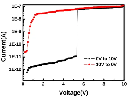
(45) measured by atomic force microscope (AFM, DI - Veeco Instruments). Every fabrication parameter is shown in Table 3-1.. Organic layer. electrode. 3x10⁻⁶ torr.. Vacuum Value Thickness. 100nm~300nm. 80nm. Evaporated rate. 0.5A/s~2A/s. 0.3~0.4A/s. Table 3-1: The parameter of fabrication process. 3.4.. Electric Characteristic Measurement The memory effect of the device is observed in I-V curves of n-type Si /Alq3/Al. sandwich device, as shown in Fig. 3-3. The I-V characteristics are recorded by applying sweeping voltage from 0V to 10V and then sweeping back to 0V. The device shows a sharp jumping current indicating the transition of the device from a low conductivity state (OFF Sate) to a high conductivity state (ON State) at a low threshold voltage (~5.3 V). This device display two distinctly different conductive states at the same applied voltage. We can give a reading voltage (below threshold voltage, ~1 V) to determine which state the device keeps. Furthermore, we can switch high conductance to low conductance by releasing the carriers trapped in the defects at the interfaces with a reverse continuous sweeping voltage (from 0 V to -10 V). That is, the device possesses the nature of electrically address memories.. 35 .
(46) 1E-7. Current(A). 1E-8 1E-9 1E-10 1E-11. 0V to 10V 10V to 0V. 1E-12 0. 2. 4. 6. 8. 10. Voltage(V) Fig.3-3: I-V characteristics of N-doped Si/Alq3/Al (semi-log plot). Current is expressed in absolute value. A small jump in the off-current was observed on the way to the off/on transition around 5.3V .. The high on/off current ratio up to 105 is obtained as shown in Fig.3-4, so that data judgment error can be easily avoided. The distinct bi-electrical states in the voltage ranging from 0 to 2.3 V allow a low voltage (e.g., 1.0 V) to read the “0” or “OFF” signal (before writing) and “1” or “ON” (after writing) signal of the device. Fig. 3-5 shows the retention time of n-type Si/Alq3/Al thin film device. As can be seen from the figure, there is no significant degradation in both states during 1000s stress test. These great properties match the demand of the trend for organic memory devices very well.. 36 .
(47) 4. 10. ON/OFF Ratio. 3. 10. 2. 10. On/Off Ratio. 1. 10. 0. 10. 0. 2. 4. 6. 8. 10. Voltage(V) Fig.3-4: The ON/ OFF current ratio as a function of applied voltage. 1E-7. Current(A). 1E-8 1E-9 ON State OFF State. 1E-10 1E-11 1E-12 0. 200. 400. 600. 800. 1000. Time(s) . Fig.3-5: The Stability test on Al/Alq3/Al device in both ON and OFF states under applied voltage of +1V continuously. 37 .
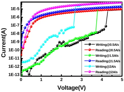
(48) 3.5.. Investigation of Deposition Rate and Thickness in organic thin film In this section, we will discuss the effect of the different deposition rate on the. device’s characteristic. In this device, the deposition rates of the Alq3 thin film are 0.05nm/sec, 0.15nm/sec and 0.2nm/sec. The rest fabrications are the same as present process that mentioned before. In the I-V characteristic curve, at first, at low bias, the devices display low conductance state (corresponding to green, black, and light blue curves in Figure 3-6). They change to high conductance state as the sweeping voltage pass threshold voltages (2.6V for high deposition rate, 3.7V for middle deposition rate, and 4.2V for low deposition rate). At next bias, the devices still hold at high conductance state in both cases (corresponding to blue, red, and pink curves in Figure 3-6). These devices exhibit two distinctly different conductance states at the same applied voltage. The high conductance and low conductance states are logic “1” and logic “0”, respectively. We can obviously find that on/off current ratio of the devices are comparable, but the conductance of the high deposition rate is higher than that of the low deposition rate. Table 3-2 displays the important parameters of the devices for both cases. Besides, we can switch high conductance to low conductance with a reverse continuous sweeping voltage (-10V to 0V or 0V to -10V).. 38 .
(49) 1E-5 1E-6. Current(A). 1E-7 1E-8 1E-9. [email protected]/s. 1E-10. [email protected]/s [email protected]/s. 1E-11. [email protected]/s. 1E-12. Writing@2A/s Reading@2A/s. 1E-13 0. 1. 2. 3. 4. 5. Voltage(V) Fig.3-6: Current-voltage relations of organic dynamic random access bistable devices with different deposition rates. (-●-), (-●-), (-●-), (-●-), (-●-), and (-●-) represent writing cycle at low deposition rate(0.5A/s), reading cycle at low deposition rate(0.5A/s), writing cycle at middle deposition rate(1.5A/s), reading cycle at middle deposition rate(1.5A/s), writing cycle at high deposition rate(2A/s), and reading cycle at high deposition rate(2A/s), respectively.. Deposition. On/Off. Current @. Ratio @ 1V. 5V. Vth Rate. Retention. Roughness. 0.05nm/sec.. 4.2V. 3.8x10⁴. 1.2x10⁻⁵. ~1000s. 0.387 nm. 0.15nm/sec.. 3.7V. 4x10⁴. 5.3x10⁻⁵. ~400s. 0.351nm. 0.2nm/sec.. 2.6V. 4.8x10⁴. 6.1x10⁻⁵. ~240s. 0.312. Table 3-2: The important parameters of the devices with different deposition rates. (Vth: threshold voltage). 39 .
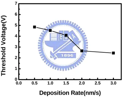
(50) Figure 3-7 shows the characteristic of the Vth versus deposition rate relations of the organic bistable device. We can find that the Vth at the lower deposition rate is much bigger then that at the higher deposition rate. It is because that the Alq3 thin film deposited at lower deposition rate is much rougher than that deposited at higher deposition rate, and AFM measurement will discuss later. If the surface of the device is much rougher, there are more traps at the surface. Therefore, we should apply higher electric field to supply the carriers to fill the traps, and then turn the device into high conductance state.. Threshold Voltage(V). 7 6 5 4 3 2 1 0 0.0. 0.5. 1.0. 1.5. 2.0. 2.5. 3.0. Deposition Rate(nm/s) Fig.3-7: Threshold Voltage-Deposition Rate relations of the organic bistable device.. 40 .
(51) Figure3-8 shows the current versus deposition rate relations of the organic bistable device. The on state current at the each deposition rate are in the same order. But the off state current at each deposition rate are apparently different. It is due to the surface roughness that we just discuss before. On the other hand, when we deposit the organic film, there are much N2 molecular in the chamber. The N2 molecular will combine with organic molecular and block the carrier injected from the electrode. Therefore, as the deposition rate decreasing, there is much time for N2 to act on with organic molecular. Hence, the off-state current will decrease when the deposited rate decreases. The on/off current ratio at different deposition rate is shown in figure 3-9. The on/off ratio is up to 104 at the lower deposition rate. It is bigger than that at the high deposition rate(~102). Hence, if we want to get a high on/off current ratio device, we should deposit the organic film slowly. In the contrast, if we want to save our fabrication time, we can deposit the film quickly, but it may cause data judging error through the reading process.. -4. OFF ON. Current(A). -6. -8. -10. -12. -14. 0. 1. 2. 3. Deposition Rate(nm/s). Fig.3-8: Current-Deposition Rate relations of the organic bistable device. (-●-) and (-●-) represent low conductance state and high conductance state respectively. A small reading bias of 1 V was applied to the device to detect the on or off state current. 41 .
(52) 7 6. ON/OFF. 5 4 3 2 1 0 0.0. 0.5. 1.0. 1.5. 2.0. 2.5. 3.0. Deposition Rate(nm/s) Fig.3-9: On/Off Current Ratio-Deposition Rate relations of the organic bistable device.. Figure 3-10 show the characteristic of threshold voltage versus Alq3 film thickness relations of the organic bistable device. It is obviously shown that the threshold voltage is increasing as the organic film is thicker. We speculate the reason is that the organic film roughness may be dependent on the film thickness. Therefore, we measure the film morphology under different thickness. We find that the organic film is rougher when the deposition rate is slow. Hence, there are more traps under the thicker organic film. Therefore, we should give higher electric field to fill the traps.. 42 .
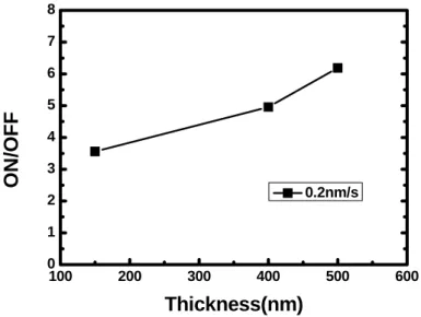
(53) Threshold Voltage(V). 7 6 5 4 3 2. 2nm/s. 1 0 100. 200. 300. 400. 500. 600. Thickness(nm) Fig.3-10: Threshold Voltage-Alq3 film thickness relations of the organic bistable device. The organic film was deposited at 0.2nm/s.. -4 -5. Current(A). -6 -7 -8. OFF ON. -9 -10 -11 -12 -13 100. 200. 300. 400. 500. 600. Thickness(nm) Fig.3-11: Current-organic film thickness of the organic bistable device. (-●-) and (-●-) represent low conductance state and high conductance state respectively. A small reading bias of 1 V was applied to the device to detect the on or off state current.. 43 .
(54) 8 7. ON/OFF. 6 5 4 3. 0.2nm/s. 2 1 0 100. 200. 300. 400. 500. 600. Thickness(nm) Fig.3-12: On/Off Current ratio of the organic bistable device. The organic film was deposited at 0.2nm/s. A small reading bias of 1 V was applied to the device to detect the on and off state current.. Figure 3-11 shows the current characteristic versus organic film thickness of the organic bistable device. In the off state, the current is decreasing as the organic film is thicker. It is because that the film is rougher as the thick organic film. In the on state, the current is increasing as the film is thicker. This is because of more traps at the interface in thicker organic film, and it can be verified by AFM measuring. These traps may enhance the on current and pass more carriers from one electrode to another electrode. The on/off current ratio versus organic film thickness is shown in figure3-12. The current ratio is increasing as the organic film is thicker. Figure 3-13 shows linear-scale current-voltage characteristics of our device deposited at 0.05nm/sec. Figure 3-14 illustrates the band diagram of our structure. They form a heterojunction and surface polarization with a transition region at the interface between N-doped Si and Alq3. This effect may affect on-sate current, as shown in figure3-13. The on-state current of Al/Alq3/Al device is a complete ohmic 44 .
(55) currrent pass thhrough the origin. o On the other hand, h the onn-state current of N-do oped Si/A Alq3/Al devvice is not a complette ohmic model. m It may m cause tthat we sh hould incrrease the vooltage to reaad the state of o the devicce.. Fig. 3-13: linear-scalle current-vvoltage charracteristics of o our bistabble device ( (a)Al/Alqq3/Al (b)N-ddoped Si/Allq3/Al )deposited at 0.005nm/s. (-■ ■-) and (-●-)) represent writing w cyclle and reading cycle, reespectively.. Fig.3-144: Band diaggram of thee proposed structure. s The differrences in thhe thresholdd voltage and a conducttivity of tw wo devices with 45 .
(56) different deposition rates may result from the difference in roughness of Alq3 thin film. That is, effective surface area between Alq3 and Al will affect directly the amount of trapping defects at the Schottky junction and then affect the voltage-current characteristic. Figure 3-15, Figure 3-16 and Figure 3-17 show AFM images of Alq3 thin film deposited at low deposition rate and high deposition rate, respectively. The corresponding mean roughnesses are 0.387 nm, 0.351 nm, and 0.312nm. This indicates that there are more traps at the interface of the former. Therefore, the former has larger threshold voltage and smaller conductivity. Besides, we can adjust electrical properties of the organic bistable devices, e.g. threshold voltage and conductivity etc., by adopting suitable deposition rates.. Fig. 3-15: The Alq3 surface morphology at 0.5A/s deposition rate. Mean roughness is 0.387nm.. Fig. 3-16: The Alq3 surface morphology at 1A/s deposition rate. Mean roughness is 0.351nm. 46 .
數據

+7

Outline
相關文件
H., “Notes on the Religious, Moral, and Political State of India before the Mahomedan Invasion, Chiefly Founded on the Travels of the Chinese Buddhist Priest Fa Hian
Each contracting State agrees that all aircraft of the other contracting States, being aircraft not engaged in scheduled international air services shall have the right, subject to
Mie–Gr¨uneisen equa- tion of state (1), we want to use an Eulerian formulation of the equations as in the form described in (2), and to employ a state-of-the-art shock capturing
A constant state u − is formed on the left side of the initial wave train followed by a right facing (with respect to the velocity u − ) dispersive shock having smaller
Attitude determines state, the state decided to state of mind.. John:I’m planning to go camping next weekend with my
Piecewise polynomial interpolation: divide the interval into a collection of subintervals and construct different approximation on each subinterval. The simplest piecewise
Then they work in groups of four to design a questionnaire on diets and eating habits based on the information they have collected from the internet and in Part A, and with
• Strange metal state are generic non-Fermi liquid properties in correlated electron systems near quantum phase transitions. • Kondo in competition with RVB spin-liquid provides
