國立交通大學
電子工程學系 電子研究所碩士班
碩 士 論 文
應用於
WiMAX 與 WiFi 傳送端並具備
補償
I/Q 未匹配與 LO 饋出之直接升頻
混波器
Direct Up-Conversion Mixer with Matching
Compensation Eliminating I/Q Imbalance and LO
Feedthrough in WiMAX and WiFi Transmitter
研 究 生 : 余宗男
指導教授 : 郭建男 教授
應用於
WiMAX 與 WiFi 傳送端並具備補償 I/Q 未匹
配與
LO 饋出之直接升頻混波器
Direct Up-Conversion Mixer with Matching Compensation
Eliminating I/Q Imbalance and LO Feedthrough in WiMAX and
WiFi Transmitter
研 究 生 : 余宗男 Student : Tsung-Nan Yu
指導教授 : 郭建男 Advisor : Chien-Nan Kuo
國 立 交 通 大 學
電子工程學系 電子研究所碩士班
碩 士 論 文
A Thesis
Submitted to Department of Electronics Engineering & Institute of Electronics College of Electrical Engineering and Computer Science
National Chiao Tung University In Partial Fulfillment of the Requirements
For the Degree of Master
In
Electronic Engineering May 2008
Hsinchu, Taiwan, Republic of China
應用於
WiMAX 與 WiFi 傳送端並具備補償 I/Q 未匹配與
LO 饋出之直接升頻混波器
學生 : 余 宗 男 指導教授 : 郭 建 男 教授
國立交通大學
電子工程學系 電子研究所碩士班
摘要
本篇論文提出具備匹配補償之升頻混波器電路,可搭配回授電路與演算法可 達到自動校正。利用向量的補償方法來使I/Q 訊號達到正交,且找出引發混波器 輸出端的本地振盪器訊號的主要原因,利用小電流源補償,使本地震盪器在輸出 端的訊號大小達到一個最小值。所有用來匹配補償的小電流源需要三十組的控制 訊號,因此我們使用序列訊號轉平行訊號的轉換器來輸入我們的控制訊號。經由 模擬驗證後可達到0.67%的 EVM。 此混波器電路利用台灣積體電路(TSMC)製程下線,整個架構包含 I/Q 混波 器、本地振盪器的四相位產生器、本地震盪器的 I/Q 緩衝器、I/Q 混波器和序列 訊號轉平行訊號的轉換器。電路的下線面積為 1.65X1.25 mm2,功率消耗為 50.4mW。 由於序列訊號轉平行訊號的轉換器電路部分發生了箝制效應,致使控制訊號 無法正確輸入且匹配補償電路無法正確工作,因此我們最後只能量測I/Q 混波器 未匹配補償的特性。量測結果顯示在 2.4GHz~2.7GHz,I/Q 混波器具有大於-11.15dB 的增益、5dBm 的 1-dB 功率增益壓縮點、大於 15dB 的無用邊帶抑制與 最大 15dB 的 LO 饋出抑制。由於無法經由電路本身最匹配補償,經由人為手動補 償後,可達到 38.5dB 的無用邊帶抑制。
Direct Up-Conversion Mixer with Matching Compensation
Eliminating I/Q Imbalance and LO Feedthrough in WiMAX
and WiFi Transmitter
Student: Tsung-Nan Yu Advisor: Prof. Chien-Nan Kuo
Department of Electronics Engineering & Institute of Electronics
National Chiao-Tung University
ABSTRACT
This thesis proposes an up-conversion I/Q mixer with matching compensation eliminating I/Q imbalance and LO feedthrough. By additional power detection feedback loop and compensation algorithm, auto-compensation can be achieved. The compensation for I/Q balance is achieved by using vectors compensation. The main factor resulting in LO feedthrough is identified and compensated by small current sources. All the small current sources used for matching compensation are controlled with thirty control signals. The thirty control signals is fed by 3-wire. From post-simulation results, the EVM with 0.67% can be achieved.
The circuit in this work is realized in TSMC 0.18um CMOS technology and composed of I/Q mixer, polyphase filter, LO I/Q buffers, and 3-wire. The total area of this chip is 1.65x1.25 mm2 and the power consumption is 50.4mW.
From measurement results, the 3-wire is failed due to latch-up. The control signals for matching compensation can’t be fed the circuit. So, the matching compensation can’t work successfully. The performance of the I/Q mixer without any
matching compensation is measured with LO frequency form 2.4GHz to 2.7GHz. The I/Q mixer is measured with conversion gain of better than -11.15dB, the 1-dB compression point of 5dBm, the unwanted sideband suppression of better than 15dB, and the maximum LO feedthrough suppression of 15dB. Since the matching compensation can’t be achieved by compensation circuit in the chip, the unwanted sideband suppression can be lowered as 38.5dB after manual compensation with tuning the magnitude and phase of baseband I/Q signals.
誌謝
得以順利完成此篇論文,首要感謝的是我的指導教授,郭建男教授,這近三 年來的悉心指導,使我體悟到許多人生的大道理。此外,感謝參與工研院計畫的 陳巍仁教授、溫文燊博士、工研院楊子毅組長,給予我相當多的建議與指導,在 此獻上最深的敬意。 感謝昶綜、鈞琳、明清、鴻源等學長們的不吝指導,在許多方面給予我非常 大的幫助;感謝一起研究、一同奮鬥、互相勉勵的俊興、燕霖,以及易耕、煥昇、 俊豪、建忠、子超、信宇等學弟們,由於有了你們,實驗室就像一個溫馨的大家 庭,非常感謝大家這兩年多來的照顧。另外還要感謝國家晶片中心在晶片製作上 所提供的協助。 最後,要特別感謝我的家人給我的栽培與鼓勵,以及女友佩詩的陪伴與打氣, 使我能順利的度過碩士生涯。還有很多其他要感謝的人,在此一併謝過。 余宗男 九十七年 五月CONTENTS
ABSTRACT (CHINESE) ... I
ABSTRACT (ENGLISH) ... III
ACKNOWLEDGEMENTS ... V
CONTENTS ... VI
TABLE CAPTIONS ... IX
FIGURE CAPTIONS ... X
CHAPTER 1 Introduction ... 1
1.1 Motivation ... 1
1.2 Thesis Organization ... 2
CHAPTER 2
EVM in Direct-Conversion Transmitter
Consideration………..3
2.1 Direct-Conversion Transmitter ... 3
2.2 Sources of Degrading EVM in General consideration ... 5
2.2.1 Intersymbol or Interchip Interference (ISI or ICI) ... 5
2.2.2 Close-in Phase Noise of Synthesized LO ...
7
2.2.3 LO Feedthrough...
8
2.2.5 Nonlinearity Influence……….12
2.2.6 Total EVM ……….13
2.3 EVM in WiFi and WiMAX ... 14
2.4 Summary ... 16
CHAPTER 3 Circuit Design for Direct
Up-Conversion Mixer with Matching Compensation
Eliminating I/Q Imbalance and LO Feedthrough in
WiMAX and WiFi Transmitter ... 17
3.1 LO-feedthrough in Up-Conversion Mixer Consideration 19
3.1.1 Factors of Inducing LO Feedthrough ... 19
3.1.2 I/Q Mixer Design for LO Feedthrough Suppression ... 21
3.2 I/Q Imbalance Compensation Circuit Design for
Up-Conversion I/Q Mixer ... 25
3.2.1 I/Q Imbalance Equivalent Model ... 25
3.2.2 I/Q Imbalance Compensation Mechanism ... 25
3.2.3 LO I/Q Buffer Design ... 28
3.3 Algorithm for I/Q Imbalance and LO Feedthrough
Compensation ... 36
3.3.1 Algorithm for LO Feedthrough Compensation ... 36
3.3.3 Algorithm for I/Q Gain Imbalance Compensation ... 41
3.3.4 Post Simulation Result with Compensation Algorithm ..
43
3.4 Summary ... 45
CHAPTER 4 Chip Measurement ... 39
4.2 Circuit Measurement……….47
4.2 Circuit Measurement……….48
4.3 Summary……….56
CHAPTER 5 Summary and Future Work ... 58
5.1 Summary ... 58
5.2 Future Work ... 59
REFERENCES ... 60
TABLE CAPTIONS
Table I Difference between 802.11 and 802.16………...……..14
Table II EVM contribution from each source………...15
Table III TSMC 0.18um technical documents for device mismatch reference……20 Table IV Performance summary of simulation results……….46
Table V Performance summary of measurement results………56
FIGURE CAPTIONS
Fig. 2.1 Block diagram of direct-conversion transmitter………..3
Fig. 2.2 Factors degrading EVM in direct-conversion transmitter………...5
Fig. 2.3 LO feedthrough induced error vector……….…………....9
Fig. 2.4 Unwanted sideband signal induced error vector……….…..11
Fig. 3.1 Proposed I/Q modulator………...……….18
Fig. 3.2 Double balanced Gilbert Cell mixer…………..………20
Fig. 3.3 Monte-Carlo analysis of LO feedthrough due to switching stage device mismatch………21
Fig. 3.4 Monte-Carlo analysis of LO feedthrough due to switching stage and transconductance stage device mismatch………...………..21
Fig. 3.5 Monte-Carlo analysis of LO feedthrough due to switching stage device mismatch with the DC current offset of the two transconductance stages 5uA...……….23
Fig. 3.6 DC current offset of the two transconductance stages device mismatch by Monte-Carlo analysis……….………23
Fig. 3.7 Proposed I/Q mixer………24
Fig. 3.8 I/Q imbalance equivalent model………25
Fig. 3.9 (a) The constellation of QPSK and the error vector. (b) The error vector analysis in I/Q plane………...………...…26
Fig. 3.10 I/Q compensation steps of (a) with original I/Q constellation point,(b) with compensating phase error of I-channel, and (c) with compensating magnitude error of Q-channel.……….……….27
Fig. 3.12 Current mode operation of Q-buffer………29
Fig. 3.13 I/Q buffer schematic………..32
Fig. 3.14 The gm of Mi1~Mi4 in response to ID1……….33
Fig. 3.15 Linear gm variation of Mi1~Mi4 along with id1………..…………33
Fig. 3.16 The linear response of ∆gm of (gmi1-gmi3) or (gmi2-gmi4) to id1……….…...33
Fig. 3.17 The gm of Mi5~Mi6 and Mq5~Mq6 in response to ID2………...34
Fig. 3.18 Frequency response to the relation of ∆gm of (gmi1-gmi3) or (gmi2-gmi4) to id1………...………34
Fig. 3.19 Frequency response to the gm of Mi5~Mi6 and Mq5~Mq6 in response to ID2………...34
Fig. 3.20 The phase and magnitude of I-buffer varying with control bits...……..35
Fig. 3.21 The magnitude of Q-buffer varying with control bits………35
Fig. 3.22 Algorithm for LO feedthrough compensation………..37
Fig. 3.23 The post simulation result of Q-mixer by using LO feedthrough compensation algorithm………...38
Fig. 3.24 The post simulation result of I-mixer by using LO feedthrough compensation algorithm……….38
Fig. 3.25 Algorithm for I/Q phase imbalance compensation………...……...40
Fig. 3.26 The post simulation result of I/Q mixer by using I/Q phase imbalance compensation algorithm………....41
Fig. 3.27 Algorithm for I/Q gain imbalance compensation……….….42
Fig. 3.28 The post simulation result of I/Q mixer by using I/Q magnitude imbalance compensation algorithm……….…...43
Fig. 3.29 The simulated spectrum by post simulation without compensating……..44
Fig. 4.1 Die micrograph………..47
Fig. 4.2 Measurement setup………48
Fig. 4.3 Layout view of D-type flip flop cell………...49
Fig. 4.4 Conversion gain varying with input power level and LO frequency……50
Fig. 4.5 Sideband suppression varying with input power level and LO frequency………...50
Fig. 4.6 LO feedthrough suppression varying with input power level and LO frequency………...………...51
Fig. 4.7 On-board baluns loss check by simulation………51
Fig. 4.8 Conversion gain varying with input power level and LO frequency after calibrating balun loss……….52
Fig. 4.9 Conversion gain versus LO frequency………52
Fig. 4.10 I/Q imbalance equivalent model II………...……..53
Fig. 4.11 Spectrum measured after phase compensation………..54
Fig. 4.12 Spectrum measured with baseband signal I-path turning on……….54
Fig. 4.13 Spectrum measured with baseband signal with Q-path turning on……55
Fig. 4.14 Spectrum after the phase and magnitude compensation………55
CHAPTER 1
Introduction
1.1 Motivation
The standard of IEEE 802.16 family, popularly known as WiMAX, provides wireless transmissions of high data rates over metropolitan areas. The transmitted signal format may include complicated modulation such as 64-QAM. To ensure correct data receiving, the measure of error vector magnitude (EVM) quantifies the error of transmitted signals and defines the performance of digital radio transmitters. It is therefore critical to minimize the EVM.
Many non-ideal circuit effects contribute to EVM degradation in RF end, including LO phase noise, carrier feedthrough, I/Q imbalance, and nonlinearity. The normal figure of transmitter circuitry achieves the level from -20dB to -25dB. In the latest released WiMAX mobile standard [1], however, it defines a severe EVM level of -30dB, much higher than that as required by other standards such as WLAN. Recently, there are some circuit calibration solutions for this issue [2] [3].
In this thesis, an open-loop compensation mechanism for I/Q imbalance and LO feedthrough in the I/Q modulator is described to meet the specifications. Combined with simple power detection in the analog circuitry and decision making in the digital circuitry, auto-calibration can be realized in the transmitter circuit
1.2 Thesis Organization
In Chapter 2, the factors degrading EVM are identified and introduced how they influence EVM. And EVM specification of WiMAX is also defined.
In Chapter 3, the I/Q modulator with compensating I/Q imbalance match and LO feedthrough is designed. Also the compensation algorithm is proposed to cooperate with the I/Q modulator.
In Chapter 4, the circuit implement and measurement results are presented. In the last Chapter, the work is summarized and concluded.
CHAPTER 2
EVM in Direct-Conversion Transmitter
Consideration
2.1 Direct-Conversion Transmitter
The direct-conversion transmitter combines the signals of I and Q channels and converts baseband signals to radio-frequency. First the baseband codes are translated to analog signals by D/A converters and low-pass filters to suppress out-band spurious noise. Then the signals of I and Q channels are up-converted to RF and combined together by I/Q modulator. Almost over 90% of transmitter gain is in the RF block from the I/Q modulator to the PA. An RF band-pass filter is inserted between the driver amplifier and the PA to suppress the out-of-band interference.
The signal level in the transmitter is normally much higher than that in a receiver, and thus the noise figure is not as critical in the transmitter as in the receiver. The important parameters for a transmitter are the output power, especially the maximum output power, and the fidelity of the transmission waveform measured by modulation accuracy, EVM. In addition to these parameters of the desired transmission signal, the unwanted emissions, such as adjacent channel power and in-band and out-band noise/spurs emissions, are usually well defined in the mobile transmitter specifications.
This Chapter focuses on EVM analysis of direct-conversion transmitter. The sources that degrading EVM are discussed below.
2.2 Sources of Degrading EVM in General Consideration
EVM may be degraded by Intersymbol or Interchip Interference (ISI or ICI), Close-in phase noise of synthesized LO, LO feedthrough, I/Q Imbalance, and Nonlinearity. These sources are induced by the circuit blocks in direct-conversion transmitter and indicated in Fig. 2.2. We can identify how they affect EVM by [1]-[3] and define the system requirements to meet the specification.Fig 2.2 Factors degrading EVM in direct-conversion transmitter.
2.2.1 Intersymbol or Interchip Interference (ISI or ICI)
Intersymbol interference (ISI) is a form of distortion of a signal in which one symbol interferes with subsequent symbols. This is an unwanted phenomenon as the previous symbols have similar effect as noise, thus making the communication less reliable. ISI is usually caused by multipath propagation and the inherent non-linear frequency response of a channel. Ways to fight against intersymbol interference include adaptive equalization and error correcting codes.
The ISI or ICI of symbols or chips may have been created at beginning to generate a transmission signal. To obtain high spectral efficiency of the transmission
signal, the originally rectangular symbol or chip waveform is reshaped, and it is also called pulse shaping. The shaped symbol (or chip) waveform aTX_ideal can be expressed
as
_ ( )
TX ideal PS rect
a =h ∗a t . (2-1) In the wireless systems, a complementary filter with an impulse response hPS_C is
normally used in the corresponding receiver side to equalize the phase and magnitude distortion and thus to eliminate or to minimize the ISI or ICI caused by the pulse shaping in the transmitter.
The filters in the transmitter path other than the pulse-shaping filter may cause the degradation of the modulation accuracy degradation especially when the pass-band of the filter, such as a channel filter, is close to the bandwidth of the transmission signal. Assuming the impulse response of the filter is hfltr(t), the shaped
symbol or chip waveform aTX_ideal after passing through the filter turns into _
( ) ( ) ( )
TX fltr TX ideal
a t =h t ∗a t . (2-2) The corresponding EVMISI can be expressed by the impulse response function as [4]
2 0 , 0 2 0 ( ) ( ) k fltr s k k ISI fltr h t kT EVM h t =∞ =−∞ ≠ + =
∑
. (2-3)The terms in the numerator in the square root of (2-3) right side are ISIs or ICIs to the symbol or chip at t0, and they are contributed from adjacent and other symbols or chips. Each term in the square root of (2-3) can be also obtained by means of the following formula:
0 0 0 0 0 0 ( ) ( ) ( ) ( ) ( ) t t fltr s fltr s t t ISI t t fltr fltr t t h t kT dt h t kT I k h t h t dt δ δ δ δ + − + − ± ± Δ ± = =
∫
∫
, (2-4)where k is equal to 1,2,3,…, and 2δt is the duration of sampling pulse. The equation (2-3) could be written as 2 ( ) ISI ICI EVM ∞ I k −∞ =
∑
Δ . (2-5)2.2.2 Close-in Phase Noise of Synthesized LO
Another main contribution to the degradation of the modulation accuracy is the close-in phase noise of the synthesizer applied as local oscillator of the up-converter in the transmitter. Assuming the vector error caused by the synthesizer phase noise n(t) can be expressed as
'( ) ( ) ( ) ( ) exp( n( ))
a tG =a tG +e tG =a tG jφ t . (2-6) The magnitude of the vector error then can be expressed as
2 2 2
( ) '( ) ( ) n
e t = a t −a t ≅φ
G G G
, (2-7) where |a(t)| is normalize to 1. The statistical average of n2(t) is the autocorrelation function of the phase noise. The autocorrelation function and the power spectrum density Sn(f) have the following relationship
{ }
/ 2 2 / 2 1 ( ) ( )lim
Ts n n Nphase n Ts E t dt S f df P nTs φ ∞ →∞ − −∞ = =∫
∫
(2-8)Hence the EVMNphase resulting from the phase noise of the synthesizers could be written as
Nphase Nphase
EVM = P . (2-9) Usually the phase noise within the loop bandwidth of synthesizers used in the mobile transmitters is in the range of -60 to -80 dBc/Hz. In the case of the synthesizer loop bandwidth being reasonable wide, PNphase could be approximated as
/10
_
2 10Nphase
Nphase synth loop
P ≅ ⋅ ⋅BW , (2-10) Where Nphase is the average phase noise, in dBc/Hz, within the synthesizer loop bandwidth, and BWsynth_loop is the bandwidth of the synthesizer loop filter in Hz. The EVMNphase in (2-4) could be modified as
/10
_
2 10Nphase
Nphase Nphase synth loop
EVM = P ≅ ⋅ BW (2-11)
The equation if (2.11) could help us to define the specification of phase noise and loop bandwidth in the system.
2.2.3 LO Feedthrough
The DC offset in the baseband I and Q channels will cause LO feedthrough, and it will degrade the modulation accuracy of the transmission signal. Assuming the dc offset in the baseband I and Q channels are ∆Idc and ∆Qdc. The baseband signal a’I(t) and a’Q(t), in the I and Q channels are respectively represented by
' ( ) cos ( )I dc
a t = φ t + Δ (2-12) I
' ( ) sin ( )Q dc
a t = φ t + ΔQ . (2-13)
At the output of the modulator, the I and Q quadrature signals turn into a signal with an RF carrier, and it can be expressed as
[
]
( ) ' ( )cos ' ( )sin ( ) cos ( ) cos( ) out I c Q c c dc c RF t a t t a t t A t t t t ω ω ω φ ω θ = − ≅ + + Δ + Δ , (2-14)2 2 ( ) cos ( ) sin ( ) A t = φ t + φ t (2-15) 1 sin ( ) ( ) tan cos ( ) t t t φ φ φ − ⎛ ⎞ = ⎜ ⎟ ⎝ ⎠ (2-16) 2 2 dc Idc Qdc Δ = Δ + Δ (2-17) 1 tan ( dc) dc Q I θ − Δ Δ = Δ (2-18) The modulated signal is shown in Fig. 2.3 and also LO feedthrough induced error vector are indicated. How LO feedthrough affecting signal constellation could clearly be found out that it also contributes an error vector.
Fig. 2.3 LO feedthrough induced error vector
Since I/Q axis of I/Q constellation is moved by the LO feedthrough term of (2-14), from Fig2.3, the <e(t)> is with the same magnitude of ∆dc and reverse
direction of ∆θ. LO feedthrough suppression (LOFTS) in dB could be defined as
10log 20log 20log
( ) Δ = LOFT = LOFT = dc TX TX P V LOFTS P V A t (2-19)
, where VLOFT is ∆dc and VTX is A(t). And then EVMLOFT which is contributed by LO
feedthrough could simply be written as
20 ( ) 10 ( ) ( ) Δ = = = = LOFTS dc LOFT LOFT TX e t V EVM V A t A t . (2-20)
So, the equation (2.20) could help us to define system specification of EVM which is degraded by LO feedthrough.
2.2.4 I/Q Imbalance
For single sideband modulation the amplitude and phase mismatches between I and Q generate unwanted sideband signal. By using ε and σ to represent amplitude and phase mismatches between quadrature LO signals, respectively. At the output of the modulator, the I and Q quadrature signals turn into a signal with an RF carrier, and it can be expressed as
[
]
[
]
2 2 1 2(1 ) cos (1 ) cos ( ) 2 1 2(1 ) cos (1 ) cos ( ) 2 out c c RF t t t t ε σ ε ω φ δ ε σ ε ω φ γ + + + + ≅ + + − + + + + − + (2-21), where δ and γ are
1 (1 )sin tan 1 (1 ) cos ε σ δ ε σ − + = + + (2-22) 1 (1 )sin tan 1 (1 ) cos ε σ γ ε σ − − − = − + . (2-23) The upper side of (2-21) is the desired signal and the lower side of (2-22) is the unwanted sideband signal. Hence the sideband suppression (SBS) in dB could be calculated as
2 2 1 2(1 ) cos (1 ) 10log 1 2(1 )cos (1 ) − + + + = + + + + SBS ε σ ε ε σ ε (2-24)
Fig 2.4 Unwanted sideband signal induced error vector
After received by the receiver, the transmitter output is converted to baseband I and Q channels as 2 2 1 2(1 ) cos (1 ) cos ( ) 2 1 2(1 ) cos (1 ) cos( ( ) ) 2 cos ( ) cos( ( ) ) I RX SB BB t t A t A t ε σ ε φ ε σ ε φ β φ φ β + + + + = − + + + + + = + + (2-25) 2 2 1 2(1 ) cos (1 ) sin ( ) 2 1 2(1 ) cos (1 ) sin( ( ) ) 2 sin ( ) sin( ( ) ) Q RX SB BB t t A t A t ε σ ε φ ε σ ε φ β φ φ β + + + + = − + + + + + = + + (2-26)
, where β is (γ-δ). The received signal constellation could be affected by the unwanted sideband signals as Fig.2.4 shown. When β is equal to zero, EVMSB which is
20 10 2 SBS SB SB RX RX e A EVM A A = = = (2-27) So, the equation (2-27) could help us to define system specification of EVM which is degraded by I/Q imbalance.
2.2.5 Nonlinearity Influence
Transmitter usually operates well below its 1-dB compression point (P-1dB). Thus,
among the nonlinear effects, the third-order intermodulation of two nearby interferers is the major EVM contributor. The input third order intermodulation interception point is inf 3 inf 3 2 o IM i P P IIP = − +P
,
(2-28) where Pinfo and Pinfi are out-band signal power in the output and input, and PIM3 arein-band interference power of the 3rd intermodulation product. Hence the interference power could be written as
3 inf 2 inf 2 3 3 inf 2 3
IM o i o
P =P + P − IIP = P − OIP , (2-29) where OIP3 is the output 3rd intercept point.
The EVM caused by 3rd intermodulation is just the square root ratio of the PIM3 to
the desired RF signal power (PRFO), as following
3 3 inf 2 3 3 20 20 3 10 10 IM RFO o RFO P P P OIP P IM IM RFO A EVM A − − − ≈ = ≈ . (2-30)
And it could be used to define the system specification.
Since the nonlinearity in the transmitter is dominated by power amplifier (PA), the distortion of PA contains the amplitude distortion (AM-AM) and phase distortion (AM-PM). And the equation (2-30) just describes the intermodulation influence.
Furthermore the EVM degraded by PA is defined clearly in [4].
2.2.6 Total EVM
If all factors contributing to the degradation of the modulation accuracy are uncorrelated, the overall EVM if the transmission signal can be expressed as
2 2 2 2 2 2 3 total k k ISI Nphase CFT SB IM EVM EVM
EVM EVM EVM EVM EVM
=
= + + + +
∑
2.3 EVM in WiFi and WiMAX
EVM requirements for 802.11 are specified at -25 dB, which is required to achieve a 10% packet error rate. For 802.16, EVM is held to -31 dB, which is based on a 1% packet error rate. This lower error rate helps contribute to WiMAX longer range. The difference between 802.16 and 802.11 is indicated in TABLE I.
TABLE I Difference between 802.11 and 802.16
WLAN (802.11) WiMAX (802.16)
Bandwidth Fixed; 20 MHz/52 Subcarriers Variable; 1 to 28MHz/256 Subcarriers
Guard Interval Fixed at 1/4 * Symbol
Time
Variable; Ranges from 1/32 to 1/4 * Symbol Time
Spectral Efficiency 2.7 Mbits/s/Hz 3.1 to 3.8 Mbits/s/Hz
EVM Requirements -25 dB -30 dB
Receive Noise Figure 10 dB Maximum 7 dB Maximum
Duplexing TDD TDD, FDD, HFDD
Spectrum Unlicensed Licensed & Unlicensed
Transmit Dynamic Range Tx Power Fixed 50-dB Range
A proper specification of sources degraded EVM are defined in Table I from [5] [6]. Since the EVM specification of 802.16 is stricter than 802.11, the RF transmitter of WiMAX could meet the requirement of WiFi by shifting carrier frequency.
From Fig. 2.2, the I/Q modulator includes two factors of degrading EVM, such as LO feedthrough and I/Q imbalance. So, in this work, I/Q modulator with eliminating LO feedthrough and I/Q imbalance are designed.
TABLE II EVM contribution from each source
Source EVM (%) EVM (dB)
ISI/ICI 0.5 -46 LO Phase Noise 2.37 -32.5 Carrier Feedthrough 0.56 -45 I/Q imbalance 1.58 -36 Nonlinearity 1 -40 Total 3.11 -30.13
2.4 Summary
The factors degrading EVM has been identified. We can realize how they degrading EVM by some circuit characteristics, such as ISI or ICI rising after passing channel filters, phase noise of synthesizer, unwanted sideband suppression, LO feedthrough suppression, and the input third order intermodulation interception point.
The specification about EVM in WiMAX is -30dB. From the circuit characteristics mentioned before, a proper specification for the factors degrading EVM and the required circuit characteristics is defined.
CHAPTER 3
Circuit Design for Direct Up-Conversion Mixer with
Matching Compensation Eliminating I/Q Imbalance
and LO Feedthrough in WiMAX and WiFi
Transmitter
The auto-compensation techniques for I/Q imbalance can be separated into two kinds of feedback loops of power detection loop [7] and dummy path for extracting error messages [8]. The power detection loop needs more iteration for achieving an optimal condition and less additional hardware. The loop with dummy path for extracting error messages can get error messages with less iteration but needs more hardware.
However, the two feedback loops need an open loop circuit to tune the I/Q magnitude imbalance and phase imbalance. In this work, I/Q modulator with an open loop compensation circuit to tune the I/Q imbalance and LO feedthrough is presented. Since LO buffers are originally needed, we design the LO buffers with magnitude and phase tuning without another hardware. An auto-compensation algorithm is developed for power detection loop with advantage of needing less additional hardware. By applying the algorithm for co-simulated with the I/Q modulator, the specification of EVM in Table II can be achieved.
The proposed I/Q modulator in this thesis is shown in Fig. 3.1. The I/Q mixer is based on conventional double balanced Gilbert Cell mixer with LO feedthrough
adjustments. Before LO I/Q signals is fed the I/Q mixer, LO buffers are placed to tune the magnitude and phase of LO I/Q signals. The two stages of polyphase filter are placed before I/Q buffer to generate quadrature LO signals for measurement consideration.
3.1 LO Feedthrough in Up-Conversion Mixer Consideration
The main advantage of double balanced Gilbert Cell mixer shown in Fig. 3.2 is LO cancellation. However, LO feedthrough accompanies imperfect LO cancellation. The LO feedthrough due to dc current offset induced by the transconductance stages (Mt+ and Mt-) device mismatch, switching stage device mismatch, and differential LOsignals imbalance, are identified in this thesis. A compensation method is developed to suppress the LO feedthrough.
3.1.1 Factors of Inducing LO Feedthrough
First, we need to identify whether the switching stage (MS1-MS4) or the
transconductance stages (Mt+ and Mt-) device mismatch of a double balanced Gilbert
Cell mixer causes a larger LO feedthrough. The switching stage (MS1-MS4) device
mismatch induces the DC current mismatch of MS1 and MS3 or MS2 and MS4. This DC
current mismatch causes imperfect LO cancellation. However, it has less impact to LO feedthrough since the double balanced mixer uses differential topology and can suppress it. The DC current offset between the transconductance stages, Mt+, and Mt-,
is induced by the transconductance stages (Mt+, Mt-) device mismatch. If the DC
current of Mt+ is larger than Mt-, it should further degrade the current matching of MS1
and MS3, or MS2 and MS4. This effect can’t just be suppressed by differential topology.
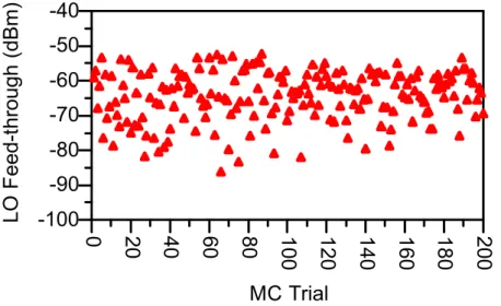
Here, the Monte-Carlo simulations of LO feedthrough use Table III which is supported in TSMC 0.18um technical documents for device mismatch reference. As Fig. 3.3 and Fig. 3.4, the switching stage (MS1-MS4) device mismatch induces small
LO feedthrough and the two transconductance stages (Mt+, Mt-) device mismatch
induces larger one. So, the main factor degrading LO feedthrough is the transconductance stages (Mt+, Mt-) device mismatch. So, the DC current offset of the
Table III TSMC 0.18um technical documents for device mismatch reference
1.8V NMOS 1.8V PMOS 3.3V NMOS 3.3V PMOS σVth0 (mV) 3.635*geo_fac 4.432* geo_fac 6.227* geo_fac 4.525* geo_fac σXL / L (%) 0.458* geo_fac 0.396* geo_fac 0.365* geo_fac 0.247* geo_fac σXW / W (%) 0.373* geo_fac 0.326* geo_fac 0.298* geo_fac 0.201* geo_fac σTox / Tox (%) 0.101* geo_fac 0.0873* geo_fac 0.0804* geo_fac 0.0543* geo_fac
Where geo_fac=1/sqrt(N*Leff*Weff) (1/um)
two transconductancestages needs to be compensated.
Besides DC current offset, there is another factor degrading LO feedthrough, the differential LO signals imbalance. The differential LO signals imbalance can be viewed as a common mode signal existing in differential LO signals. Since the source couple pair is with high common mode rejection ratio, the LO cancellation could be almost perfect. However, the differential LO signals imbalance could still enlarge LO feedthrough when the MS1-MS4 or the two transconductancestages (Mt+, Mt-) are with
device mismatch. If the DC current offset of the two transconductancestages can be compensated, the differential LO signals imbalance can be ignored.
20 40 60 80 100 120 140 160 180 0 200 -90 -80 -70 -60 -50 -100 -40 MC Trial LO F eed-t hrough (dBm )
Fig. 3.3 Monte-Carlo analysis of LO feedthrough due to switching stage device mismatch 20 40 60 80 100 120 140 160 180 0 200 -90 -80 -70 -60 -50 -40 -30 -20 -10 -100 0 MC Trial LO F eed-t hrough (dBm )
Fig. 3.4 Monte-Carlo analysis of LO feedthrough due to switching stage and transconductance stage device mismatch
3.1.2 I/Q Mixer Design for LO Feedthrough Suppression
Gilbert cell is used for I/Q mixer topology with resonant loads of LC tanks and current summation for combining I-channel and Q-channel signals as shown in Fig.3.7.The I/Q mixer is designed with IIP3 of 10dBm and conversion gain of -7dB at LO power of 6dBm. The total power consumption of I/Q mixer is 13.8mW.
The DC current offset resulting from device mismatch of the two transconductance stages needs to be suppressed to lower LO feedthrough. A compensating circuit with IDACs has applied to compensate DC current offset of the two transconductance stages in the I/Q mixer, as shown in Fig.3.7. The two switches of MIS+ and MIS- or MQS+ and MQS- decide which transconductance stage of MIt+ and
MIt- or MQt+ and MQt- has less current and needs to be compensated. Since the IDACs
have quantization error, the compensation of DC current offset is imperfect. The optimal resolution of the IDACs needs to be identified and ensures the quantization error of it doesn’t degrade LO feedthrough too much.
The I/Q mixer is designed with output signal of 0dBm, since it has good linearity. From Table II, LO feedthrough needs 45dB suppression relating to desired signal. Since the desired signal power of the I/Q mixer in this work is 0dBm, the LO feedthrough needs to be designed below -45dBm. By using the standard deviation of device mismatch in Table III for Monte-Carlo analysis, the maximum allowed DC current offset between the two transconductance stages can be identified. From the result shown in Fig.3.5, the DC current offset between the two transconductance stages needs to be set below 5uA to obtain LO feedthrough of -45dBm. On the other hand, the quantization error and the resolution of the IDAC have a maximum value of 5uA and 10uA. Besides, the maximum DC current offset of the two transconductance stages can be obtained by Monte-Carlo analysis of the two transconductance stages device mismatch. As the result of Fig.3.6 shown, the maximum DC current offset is 80uA. Two 4-bit IDACs are used to provide the compensation current with 0~150uA to cover the maximum DC current offset and each bit resolution is 10uA in the I/Q mixer.
imperfect LO cancellation, and LO feedthrough is generated. An inverse phase of LO feedthrough can be induced by using IDACs and then compensate it.
Since the DC current offset is with the order of 10-6 ampere, it’s hardly to sense the current difference between the two transconductance stages. In this work, a compensation algorithm is used to directly detect the power of LO feedthrough and find the optimal compensation current with minimum power of LO feedthrough. This algorithm is discussed in session 3.4.1.
20 40 60 80 100 120 140 160 180 0 200 -50 -40 -60 -30 MC Trial LO F eed-t hrough (dBm )
Fig. 3.5 Monte-Carlo analysis of LO feedthrough due to switching stage device mismatch with the DC current offset of the two transconductance stages 5uA
20 40 60 80 100 120 140 160 180 0 200 -50 0 50 -100 100 MC Trial D C C urrent Of fs et (uA)
Fig. 3.6 DC current offset of the two transconductance stages device mismatch by Monte-Carlo analysis
Fig. 3.7 Proposed I/
3.2 I/Q Imbalance Compensation Circuit Design for
Up-Conversion I/Q Mixer
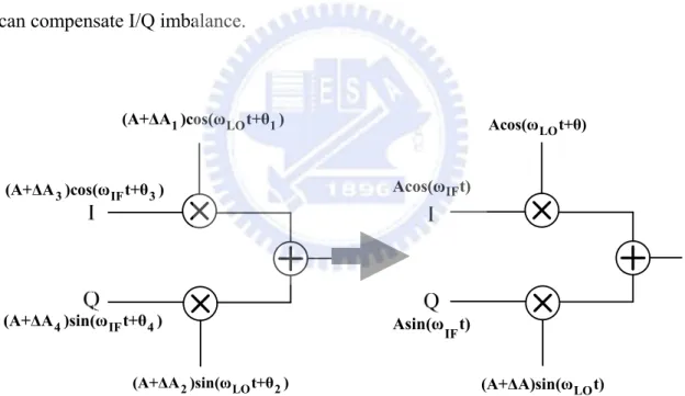
3.2.1 I/Q Imbalance Equivalent Model
In homodyne system, the up-converter is composed of I/Q mixer, I/Q LO, and summation circuit. Both imbalance I/Q baseband signals and imbalance I/Q LO signals bring magnitude and phase mismatches to the I/Q modulator. The mismatch model of I/Q modulator is shown as Fig.3.8. After some calculations, all the non-ideal effects due to both baseband and LO signals can be all refer to LO only, as indicated in Fig.3.8. So by adjusting the magnitude of LO Q-path and phase of LO I-path, we can compensate I/Q imbalance.
1 LO 1 (A+ΔA )cos(ω t+θ ) 2 LO 2 (A+ΔA )sin(ω t+θ ) 3 IF 3 (A+ΔA )cos(ω t+θ ) 4 IF 4 (A+ΔA )sin(ω t+θ ) LO Acos(ω t+θ) LO (A+ΔA)sin(ω t) IF Acos(ω t) IF Asin(ω t)
Fig. 3.8 I/Q imbalance equivalent model
3.2.2 I/Q Imbalance Compensation Mechanism
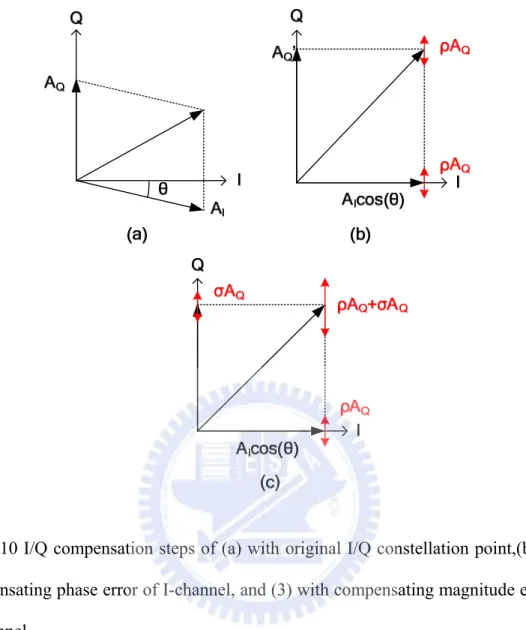
I/Q mismatch could be compensated by adding some vector on I or Q path. A simple I/Q constellation of QPSK is shown in Fig.3.9(a). In this work, both the magnitude and phase mismatch will be manipulated using magnitude compensation.
Fig. 3.9 (a) The constellation of QPSK and the error vector. (b) The error vector analysis in I/Q plane
For example, from Fig.3.9(b) the I-channel signal accrue with non-quadrature phase error relating to Q-channel. This phase error is mainly generated by <eQ> and could
be taken away by tacking on some Q-channel signal which is with equal magnitude of <eQ> and in reverse direction of <eQ>. An error vector <e1> can be referred to I-axis
and it can be thought as I channel signal induces magnitude error onto Q channel. If this mismatch needs to be removed, we can increase Q-channel magnitude by ||<eI>||.
Applying this mechanism, all magnitude and phase imbalance could be removed. I/Q imbalance compensation method is separated into three steps in this work. In Fig.3.10(a), first, the original I/Q constellation shows mismatch is appeared and the Q-path signal is set to be phase reference. Second, there is non-quadrature phase error in the I-path, so the I-path signal is added by some ratio of the Q-path signal to compensate its phase and this phase error can be removed as shown in Fig.3.10(b). During phase compensation, magnitude mismatch arises, so the final step is to adjust the Q-path magnitude equal to the I-path, shown in Fig.3.10(c). Through these three steps I/Q imbalance could be removed.
Fig. 3.10 I/Q compensation steps of (a) with original I/Q constellation point,(b) with compensating phase error of I-channel, and (3) with compensating magnitude error of Q-channel.
Since digital control is used, the resolution of each control bit needs to be defined. If each control has resolution of ∆ε, the compensation method has compensation error of ∆ε/2. From Fig.3.10(c), if magnitude and phase adjustments have compensating resolution of σAQ and ρAI, the compensation error from resolution of digital control is
(ρAI+σAQ)/2. The specification of EVM contributed by I/Q imbalance is set to be
1.58% in Table II. From EVM fundamental equation calculations, we can get:
(
)
/2 1.58% 2 cos Q I A A σ ρ θ + ≤ (3-1)If the maximum phase error θ is supposed to 15˚, the Eq.(3-1) above could be simplified as ( ) ( ) 4.32% + ≈ + ≤ Q I A A σ ρ σ ρ (3-2)
The σ and ρ are designed as 2% and 0.7% respectively for over-designed. EVM from σ and ρ chosen in this work can be 0.95% by Eq.(3-3). From Eq.(2-27), the unwanted sideband suppression can be calculated as -40.4dB relating to desired signal.
(
)
/2 2 cos + = Q I A EVM A σ ρ θ (3-3)3.2.3 LO I/Q Buffer Design
Since the I-path of LO needs to be added by the ratio of ρ to Q-path to achieve I/Q phase imbalance compensation for I-buffer, the current mode operation is used as shown in Fig.3.11. The voltages of LOI and LOQ are translated to currents by
transconductance stages and then summed at the output node. The load of ZL is put in
the output node to translate the current to voltage again. From foregoing analysis, the Gm2 needs to be with the resolution of ρGm1. The magnitude compensation for
Q-buffer also uses this scheme as shown in Fig.3.12. The ΔGm3 needs to be with the
resolution of σGm3.
The LO I/Q buffers in Fig. 3.13 is designed to achieve the schemes discussed above. In I-buffer three source couple pairs act two different characteristics in I- or Q-buffer in Fig. 3.13. The two source couple pairs of Mi1 and Mi4 or Mi2 and Mi3 are
with different bias current by IDACs of id1 to generate ∆gm between Mi1 and Mi3 or
Mi2 and Mi4 as the same as Gm2 in Fig. 3.11. The other one of Mi5 and Mi6 is offered
and Mq6 is with linear gm to IDACs of id2 as the same as Gm3 in Fig. 3.12. The I-path of
LO in Fig.3.13 is without any effect since the two source couple pairs of Mq1 and Mq4
or Mq2 and Mq3 are with identical bias current.
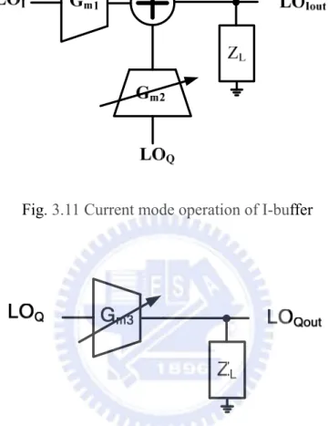
Fig. 3.11 Current mode operation of I-buffer
Fig. 3.12 Current mode operation of Q-buffer
The I/Q imbalance due to loading effect produced by I/Q buffers can be ignored since they are identical. In I-buffer, Q-path signal is combined with I signal to tune the phase of I-path. Complementary IDACs of ±id1 drive the two source couple pairs to
get small gm variation of Q signal in I buffer. Hence we can get Iout from Eq.(3-4).
(
1 3)
52 2
out Q mi mi I mi L
I =⎣⎡A ⋅ g −g + ⋅A g ⎦⎤⋅R (3-4)
, where gmi1 and gmi3 are gm of Mi1 and Mi3, respectively. The two 4-bit control
resolution of the IDACs needs to be set to make gmi1 and gmi3 as Eq.(3-5) shown
(
gmi1−gmi3)
/gmi5 =ρAQ/AI ≈2% (3-5)However, the resolution of IDACs roughly make the phase vary with 1˚ from Eq.(3-6) 1
sin (2%) 1.1− ≈ ° (3-6) Q buffer are implemented by exchanging the input signals of I buffer, as shown in Fig. 3.13. Since the I-path of Q buffer is without DC current variation and gmq1 and
gmq3 are always the same, the I-path contributing to Qout is equal to zero. And the
source couple pair of Mq5 and Mq6 is used to achieve variable magnitude function of
the Q-path signal by changing the IDAC of id2. The resolution of the IDAC controls
gm variation with
5/ 5 2 / (0) 0.7%
m mq Q Q
g g σA A
Δ = = (3-7)
Since the IDAC needs to be bidirectional to increase or decrease the Δgm5, the 10-bit
control signal is designed to control this bidirectional IDACs.
The gm of Mi1~Mi4 in response to ID1 is shown in Fig.3.14. There are three
biasing regions to choose. In the high slope region the ∆gm is large with high
sensitivity to ID. The power consumption can be saved for Mi1~Mi4 but not the case
for Mi5~Mi6. With the larger ∆gm the gmi,q5 and gmi,q6 should also be larger in response.
This leads to even larger power consumption. Meanwhile, the id1 needs to be small
enough to obtain the desired linear variation. The low slope region is also undesired with the high biasing current but insufficient compensation capability. Consequently, the medium slope region is a preferred choice.
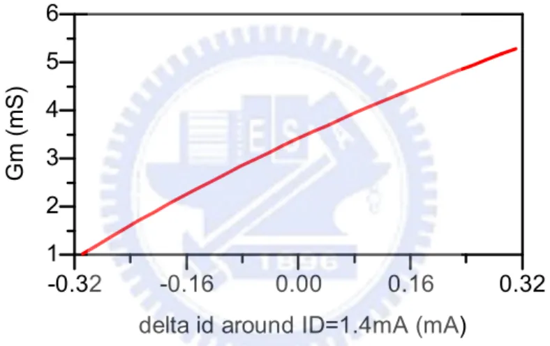
-0.32~0.32 mA is achieved by a source couple pair with tail current of 1.4mA, as shown in Fig.3.15. Fig.3.16 shows the linear response of ∆gm of (gmi1-gmi3) or
(gmi2-gmi4) to id1. Two 4-bit IDACs are used for both directional tuning, such that each
direction has 15 tuning steps. For the dynamic range of 0.32mA the current increases by 21uA for each step. The resolution of the IDACs is set as 21uA. The ∆gm versus
control bits are with slope of 0.28mS/bit. With ∆gm decided, the gmi5,6 is set as 14 mS
from Eq.(3.8) and Fig. 3.17.
5,6 / 2% 14
i m
gm = Δg = mS (3-8)
The value of ID1 has been designed accurate as above. Then the parasitic effects
in high frequency operation should be considered. In respect of this, the value of ID2
needs to be fine tuned without changing ID1 and id1. Fig.3.18 and Fig.3.19 shows the
simulation results for high frequency operation. The optimal ID2 setting is found at
1.8mA, fulfilling the requirement of Eq.(3-7).
Fig.3.19 shows the linear gm variation with ID2 as ID2 being around 1.8mA. Hence
the ID2 can be used for magnitude tuning in Q buffer. From Eq.(3-2-5) each ID2 tuning
step for magnitude tuning is set as 0.7%. With this setting simulation result shows the gmq5 variation to ID2 as 2.022mS/mA. Consequently, the id2 in Q buffer is set as 20uA.
The final I/Q buffer simulation results are shown in Fig.3.20 and Fig.3.21, for the phase tuning of I-buffer and the magnitude tuning of Q-buffer, respectively. Each step of phase tuning and magnitude tuning are 1° and the ratio of 0.07. In later section the LO I/Q buffer are combined with the I/Q mixer and the compensation algorithm are used to implement the I/Q imbalance compensation.
Fig. 3.13 I/Q buf
1 2 3 4 0 5 5 10 0 15 ID1 (mA) G m o f Mi 1 ~ Mi 4 (ms )
Fig. 3.14 The gm of Mi1~Mi4 in response to ID1
Fig. 3.15 Linear gm variation of Mi1~Mi4 along with id1
-0.16 0.00 0.16 -0.32 0.32 1 2 3 4 0 5
delta id around ID=1.4mA
(G mi 1 -G m i3 ) (mS )
Fig. 3.16 The linear response of ∆gm of (gmi1-gmi3) or (gmi2-gmi4) to id1
-0.16 0.00 0.16 -0.32 0.32 2 3 4 5 1 6
delta id around ID=1.4mA (mA)
Gm
(
m
Fig. 3.17 The gm of Mi5~Mi6 and Mq5~Mq6 in response to ID2 -0.16 0.00 0.16 -0.32 0.32 0.5 1.0 0.0 1.5
delta id around ID1=1.4mA
de lta G m ( m S )
Fig. 3.18 Frequency response to the relation of ∆gm of (gmi1-gmi3) or (gmi2-gmi4) to id1
2 4 6 8 0 10 2 4 6 8 10 0 12 ID2 (mA) Gm 5 ,6 ( m S )
Fig. 3.19 Frequency response to the gm of Mi5~Mi6 and Mq5~Mq6 in response to ID2
2 4 6 8 0 10 5 10 15 0 20 ID2 (mA) Gm i5 ,6 ( m S) 14mS
0.99 1.00 1.01 1.02 1.03 1.04 1.05 1.06 1.07 -16-14-12-10 -8 -6 -4 -2 0 2 4 6 8 10 12 14 16 -16 -14 -12 -10-8 -6 -4 -20 2 4 6 8 10 12 14 16
Phase Varying (degree)
Phase Control Bit
Magn
itude
Varying Ratio
Fig. 3.20 The phase and magnitude of I-buffer varying with control bits
-32-28-24-20-16-12 -8 -4 0 4 8 12 16 20 24 28 32 0.80 0.85 0.90 0.95 1.00 1.05 1.10 1.15 1.20 Ma g n itude V ar ying Ra ti o
Magnitude Control Bit
3.3 Algorithm for I/Q Imbalance and LO Feedthrough
Compensation
The compensation algorithm is with the order of LO feedthrough, I/Q phase imbalance, and I/Q magnitude imbalance. Since the I/Q phase imbalance causes magnitude of I-path varying simultaneously. It needs to put the I/Q phase imbalance compensation before I/Q magnitude imbalance compensation.
3.3.1 Algorithm for LO Feedthrough Compensation
In LO feedthrough compensation mode, an extra closed loop needs to be designed with pre-amplifier, power detector, sample-and-hold circuit, and comparator. Baseband signals are not to be fed the I/Q mixer. So LO signals at output node can directly be detected by PD. First, the initial LO feedthrough is detected by PD and sampled and held by S/H. Second, the IDAC of the I/Q mixer is changed with one bit of LSB (less significant bit), and LO feedthrough is detected by PD. Since the previous state of PD output is held in S/H, the comparator can be used for deciding which one is larger. With this method, the direct aspect of decreasing the bits of IDACs or increasing the bits of IDACs can be identified, and also which sides of MIt+
and MIt- or MQt+ and MQt- in Fig.3.7 needs to be compensated. The completed
algorithm is indicated in Fig.3.22. The algorithm would stop when the comparator switches the polarity. This means it has found the optimal compensating current for minimizing LO feedthrough in previous state and in the current state LO feedthrough is enlarged by undesired compensation current. So, this algorithm could find the minimum values of LO feedthrough under the condition of no baseband signals.
3.1.2, the post-simulation uses this algorithm to get a minimum LO feedthrough. First, the Q-mixer is compensated with the bit number of IDACs from initial 0 to 10 as Fig.3.23 shown. Second, the I-mixer is compensated with bit number of IDACs from initial 0 to 10 as Fig.3.24 shown. After compensation, a -60dBm power of LO feedthrough can be obtained.
-16 -12 -8 -4 0 4 8 12 16 -50 -45 -40 -35 LO Feedt hrough Power (dBm)
BCD of LO-feedthrough Suppression Control Bits (Q) Q Mixer
Fig. 3.23 The post simulation result of Q-mixer by using LO feedthrough compensation algorithm -16 -12 -8 -4 0 4 8 12 16 -65 -60 -55 -50 -45 -40 -35 LO Feedthroug h Power (dBm)
BCD of LO-feedthrough Suppression Control Bits (I) I Mixer
Fig. 3.24 The post simulation result of I-mixer by using LO feedthrough compensation algorithm
3.3.2 Algorithm for I/Q Phase Imbalance Compensation
The phase imbalance generally is hardly to be directly sensed since the signal is up to Giga hertz and I/Q signal has been combined at the output of I/Q mixer. If an
extra path is created to help sense the phase difference, the path might contribute gain imbalance or phase imbalance simultaneously. In this work two sets of baseband test signals are used without extra hardware in RF block to avoid another imbalance contribution. By feeding baseband signals of I-path and Q-path with two in-phase signals and two reverse-phase signals, the error message would appear in the form of magnitude as indicated in Eq.(3-9) and Eq.(3-10).
(
)
(
)
( , )
1 1
cos cos( ) cos sin
1/ 2 1 sin cos tan (1 sin ) / cos
1/ 2 1 sin cos tan (1 sin ) / cos
= − − = ⋅ + + ⋅ ⎡ ⎤ = ⋅ − ⋅ ⎣ − + − ⎦ ⎡ ⎤ + ⋅ − ⋅ ⎣ + + − ⎦ IQ A A IF LO IF LO LO IF LO IF RF t t t t t t ω ω θ ω ω θ ω ω θ θ θ ω ω θ θ (3-9)
(
)
(
)
( , ) 1 1cos cos( ) cos sin
1/ 2 1 sin cos tan (1 sin ) / cos
1/ 2 1 sin cos tan (1 sin ) / cos
= − − − = ⋅ + − ⋅ ⎡ ⎤ = ⋅ + ⋅ ⎣ − − + ⎦ ⎡ ⎤ + ⋅ + ⋅ ⎣ + − + ⎦ IQ A A IF LO IF LO LO IF LO IF RF t t t t t t ω ω θ ω ω θ ω ω θ θ θ ω ω θ θ (3-10)
The phase error appears as (1-sinθ) and (–(1+sinθ)) and affect their magnitude. S/H and comparator could be used for detecting the two different output signals and distinguishing which one is larger. First, the output power is detected by PD and held by S/H with in-phase baseband signals of (A, A). Second, the output power is detected by PD with reverse-phase baseband signals of (A, -A). Since the previous state of PD output is held in S/H, the comparator can be used for deciding which one is larger. If the case of in-phase baseband signals of (A, A) is with larger/ smaller power, the phase of I-path needs to be increased/ decreased by IDACs of LO I-buffer. When compensating the phase in the direct aspect, the power difference between these two vectors would be decreased. Repeat these steps until the comparator switches the polarity. This means it has found the optimal compensating current for minimizing phase imbalance in previous state and phase imbalance is enlarged by undesired
compensating current in the current state. However, another advantage of the method by using the test vectors is the information of phase error could indirectly be calculated by (3-11) and (3-12) when circuit measurement. The completed algorithm is shown in Fig.3.25. ( , ) ( , ) 1 sin | | 10 log( ) 1 sin − − − = Δ = + A A A A P dBm P dBm P θ θ (3-11) 10 1 10 1 10 sin 1 10 Δ − Δ − = + P P θ (3-12)
-16 -12 -8 -4 0 4 8 12 16 -5 -4 -3 -2 -1 0 1 2 Power Differ e n ce between
(A,A) and (A,-A) (dB)
BCD of Phase Control Bits
Fig. 3.26 The post simulation result of I/Q mixer by using I/Q phase imbalance compensation algorithm
The post-simulation result is shown in Fig.3.26. The initial power different due to phase imbalance is -1.7dB and the case of in-phase baseband signals of (A, A) is with smaller power. So, the bit number of the IDAC of LO I-buffer is decreased. With bit number of -10, the minimum phase difference can be obtained. From Eq.(3-12), the initial phase error can be obtained as 11°. Since each bit of phase compensation can adjust the phase with 1°, the compensating phase of the post-simulation is 10°. So, the Eq.(3-12) is pretty correct.
3.3.3 Algorithm for I/Q Gain Imbalance Compensation
In gain imbalance calibration, baseband test signals are needed. Since I/Q gain imbalance is wanted to detect, the baseband signals of I/Q path could be respectively fed with another path shutting down. Since I-path is used for magnitude reference, S/H and comparator can be used for distinguishing which path of I or Q is with larger
magnitude. First, the magnitude of I-path is detected by PD and sampled and held by S/H. Second, the magnitude of Q-path is detected by PD. Since the previous state of PD output is held in S/H, the comparator can be used for deciding which one is larger. Third, if the magnitude of Q-path is smaller or larger, the bit number of IDACs of LO Q-buffer is increased or decreased to get larger or smaller magnitude. Then, repeat these steps until the comparator switching the polarity. This means it has found the optimal compensating current for minimizing magnitude difference in previous state and in the current state magnitude difference is enlarged by undesired compensating current. The completed algorithm is shown in Fig.3.27.
The post-simulation result is shown in Fig.3.28. The initial magnitude different is 1dB and the Q-path is with smaller magnitude. So, the bit number of IDACs of LO Q-buffer is increased. With bit number of 11, the minimum magnitude difference can be obtained.
-32 -24 -16 -8 0 8 16 24 32 -4 -2 0 2 Power Diffe rence between I and Q Path (d B)
BCD of Magnitude Control Bits
Fig. 3.28 The post simulation result of I/Q mixer by using I/Q magnitude imbalance compensation algorithm
3.3.4 Post Simulation Result with Compensation Algorithm
Due to routing difference and mismatch, the LO feedthrough can be suppressed as 32.61dB and the unwanted sideband can be suppressed as 20dB relating to signal power as Figure.3.29 shown.
After finishing the compensation algorithm above, the LO feedthrough can be suppressed as 59dB and the unwanted sideband can be suppressed as 43.54dB relating to signal power as Figure.3.30 shown. The EVM could be calculated as 0.67% by Eq. (2-31).
2.57 2.58 2.59 2.60 2.61 2.62 2.63 2.64 2.56 2.65 -100 -80 -60 -40 -20 -120 0 Freq (GHz) O u tp u t Po w e r ( d B m )
Fig. 3.29 The simulated spectrum by post simulation without compensating
2.57 2.58 2.59 2.60 2.61 2.62 2.63 2.64 2.56 2.65 -100 -80 -60 -40 -20 -120 0 Freq (GHz) O u tp u t Po w e r ( d Bm )
3.4 Summary
Since double balanced mixers are with perfect LO cancellation, some factors of device mismatch, DC current offset, and imbalance LO can degrade LO cancellation and induce LO feedthrough. The main factor is the DC current offset due to the transconductance stages device mismatch and the DC offset from baseband signals. By using two sets of IDACs in the I/Q mixer, the DC current offset can be compensated. The LO feedthrough can be suppressed below -45dB relating to desired signal power after compensation.
A simple I/Q imbalance model has been translated in Fig.3.8. We can adjust the phase of LO I-path and the magnitude of LO Q-path to achieve I/Q matching. Since the digital control is used, the resolution of tuning phase and magnitude for I-buffer and Q-buffer needs to be proper defined. In this work, after choosing proper resolutions, the sideband signals can be suppressed below -40dB relating desired signal power.
The direct up-conversion I/Q mixer, LO buffers, and the two IDACs in the I/Q mixer form an open loop for compensation. An algorithm is needed to achieve a feedback loop by additional pre-amplifier, power detector, sample-and-hold, and comparator for auto-compensation. The algorithm is developed in this work without feedback loop implement, and is verified by co-work with post simulation.
TABLE IV Performance summary of simulation results Performance
Technology TSMC CMOS 0.18um
DC Supply Voltage 1.8 V
LO power 4 dBm
Voltage Conversion Gain -7 dB
P-1dB -6 dBm
IIP3 10 dBm
Error Magnitude Tunable Region 0.8~1.2 (per Step 0.07) Error Phase Tunable Region -15°~15°(per Step 1°)
Sideband Suppression >40dBc
LO Feedthrough Suppression >50dBc
CHAPTER 4 Circuit Implement and Measurement
4.1 Circuit Implement
The I/Q up-conversion mixer is fabricated with TSMC 0.18um technology. The die micrograph of the I/Q up-conversion mixer is shown in Fig 4.1. This circuit contains a polyphase filter, I/Q mixer, LO buffers, and 3-wire for feeding control signals. Besides, the ESD I/O pads are placed before the 3-wire inputs which are VDD, GND, Din, CLK, Clear, and Enable.
4.2 Circuit Measurement
The measurement setup is shown in Fig. 4.2. All the pads in the chip are connected to PCB by bond-wire. The input signals of 3-wire is fed by Labview and the printer port (parallel port) in PC. Since differential topology is used in this circuit, the signals of LO and IF need on-board baluns to be translated into differential signals. The RF outputs also need an on-board balun to be translated into single-end signals. Finally, the spectrum analyzer is used to measure the power of wanted signal, LO feedthrough, and unwanted sideband.
Chip on Board LO Balun IFQ Balun IFI Balun RF Balun Computer & Labview Printer Port3 Agilent Signal Generator 1 Agilent Signal Generator 2 Agilent Spectrum Analyzer To 3-Wire Agilent Signal Generator 3
Fig. 4.2 Measurement setup.
For the sake of placing few vias or contacts between the two metal layers or the diffusion and the metal 1 layer as Fig.4.3 shown, the resistance between them becomes too large, so that the 3-wire circuit is latched-up. When VDD of the 3-wire is fed with 1.8V, large DC current of 43mA occurs and the function of the 3-wire fails.
Hence the control signals can’t be fed the I/Q up-conversion mixer. However, the performance of I/Q mixer without any compensation could just be measured.
Fig. 4.3 Layout view of D-type flip flop cell
The measurement results of the conversion gain, unwanted sideband suppression, LO feedthrough suppression varying with input power level and LO frequency 2.4GHz to 2.7GHz are shown in Fig.4.4, Fig.4.5, and Fig.4.6. The P-1dB can be
identified from Fig.4.4, and is 5dBm. The conversion gain measured degrades much than the simulation results. After the on-board baluns characteristics have been measured by 4-port measurement and saved as touchstone file, they can be put together with circuit simulation. From simulation results, the conversion gain degraded by on-board baluns could be identified. In Fig. 4.7, the result of the circuit simulation with measured on-board baluns degrades the conversion gain with 15.5dB than the one with ideal baluns. We modify the measured conversion gain with adding the on-board baluns loss of 15.5dB and get Fig. 4.8 at 2.6GHz. After all, the conversion gain is higher than -11.15dB with LO frequency from 2.4GHz to 2.7GHz. The conversion gain versus LO Frequency is shown in Fig. 4.9. The resonant frequency of mixer output LC tank is shifted relating to original design with resonant frequency of 2.5GHz.
-15 -10 -5 0 5 10 -35 -30 -25 -20 -15 Co nv ersi o n G ai n ( d B) powerin (dBm) 2.4GHz_Measured 2.5GHz_Measured 2.6GHz_Measured 2.7GHz_Measured
Fig. 4.4 Conversion gain varying with input power level and LO frequency
-10 -5 0 5 10 15 10 15 20 25 SBS (dBm) IF Power in (dBm) 2.4G_SBS 2.5G_SBS 2.6G_SBS 2.7G_SBS
-10 -5 0 5 10 15 -20 -15 -10 -5 0 5 10 15 LO FTS (dB ) IF Power in (dBm) 2.4G_LOFTS 2.5G_LOFTS 2.6G_LOFTS 2.7G_LOFTS
Fig. 4.6 LO feedthrough suppression varying with input power level and LO frequency -15 -10 -5 0 5 10 -35 -30 -25 -20 -15 -10 -5 Co nv ersi o n G ai n ( d B) powerin (dBm) 2.6GHz_Post-Sim_with Measured On-Board Balun
2.6GHz_Post-Sim_with Ideal Balun
Fig. 4.7 On-board baluns loss check by simulation 15.5dB
-15 -10 -5 0 5 10 -25 -20 -15 -10 -5 0 Conv er si on Gai n (dB) IF Power (dBm) Meaured_2.6GHz with Calibrating On-Board Balun Loss
SS_2.6GHz_Post-Sim_ with Ideal Baluns
TT_2.6GHz_Post-Sim_ with Ideal Baluns
Fig. 4.8 Conversion gain varying with input power level and LO frequency after calibrating baluns loss
2.3 2.4 2.5 2.6 2.7 -14 -12 -10 -8 -6 -4 -2 0 Conv er sion G ain ( dB) LO Frequency (GHz)
The LO I/Q signals is generated by a two-stage polyphase filter, so we can verify the design by tuning the phase and magnitude of LO signals. An equivalent model can be used for verifying our design as Fig.4.10 shown. We can adjust the phase and the magnitude of baseband I/Q signal to verify our design.
1 LO 1 (A+ΔA )cos(ω t+θ ) 2 LO 2 (A+ΔA )sin(ω t+θ ) 3 IF 3 (A+ΔA )cos(ω t+θ ) 4 IF 4 (A+ΔA )sin(ω t+θ ) IF Acos(ω t+θ) IF (A+ΔA)sin(ω t) LO Acos(ω t) LO Asin(ω t)
Fig. 4.10 I/Q imbalance equivalent model II
Use another die for measurement. After adjust the phase between the baseband I/Q signals to compensate the phase imbalance, the sideband suppression can achieve 14.3dB and the LO feedthrough suppression can achieve 40dB as Fig.4.11 shown. The magnitude compensation works after the phase compensation. With the algorithm mentioned in session 3.5.3, the spectrum of only I-path or Q-path baseband signals fed is shown in Fig.4.12 and Fig 4.13. The power difference between I-path and Q-path is 3.4dB. After enlarging the power of I-path with 3.4dB, the sideband suppression can achieve 38.5dB as Fig. 4.14. From Eq.(2-31), the EVM is 1.77% and meet the specification. If the 3-wire is on working, we ensure that a pretty good performance could be measured.
Fig. 4.11 Spectrum measured after phase compensation
Fig. 4.13 Spectrum measured with baseband signal with Q-path turning on