國 立 交 通 大 學
電機與控制工程研究所
碩士論文
One-Push 方法於多角度三維 SOI 微結構組裝之
應用
Assembly of Three Dimensional
Microstructures with Multiple Angles by
One-Push Method on SOI Wafers
研究生 :吳昌修
指導教授:邱一 博士
One-Push 方法於多角度三維 SOI 微結構組裝之
應用
Assembly of Three Dimensional
Microstructures with Multiple Angles by
One-Push Method on SOI Wafers
研 究 生:吳昌修
Student: Chang Shiou Wu
指導教授:邱一
Advisor: Yi Chiu
國立交通大學 電機學院
電機與控制工程研究所
碩士論文
A Thesis
Submitted to Department of Electrical and Control Engineering
College of Electrical Engineering
National Chiao Tung University
In Partial Fulfillment of the Requirement
For the Degree of
Master
In
Electrical and Control Engineering
November 2008
Hsinchu, Taiwan, R.O.C.
中華民國九十七年十一月
中文摘要
中文摘要
中文摘要
中文摘要
近年來在半導體產業的發展之下,微機電製程技術有許多重大的發
展。在眾多領域中對於三維微結構的要求也與日俱增,尤其在光學方面的
應用對於三維微結構的角度定位要求相當嚴格。
我們最終目標為設計一微光學資訊儲存平台,因此需要精密的角度定
位微結構。為了符合光學鏡面平坦度需求,因此利用
SOI (Silicon On
Insulator)基版上的單晶矽製造微鏡面,避免其他材質在製程中因為應力而
產生翹曲。此外,我們亦將使用
SU-8 當結構層來製造出平面微結構,由
於
SU-8 有良好的機械特性和低溫製程,可使往後的電路整合更加容易。
本實驗室之前已提出利用單一下壓動作 (One-Push) 即可使微鏡面成
功的組裝在
90° 的設計,本論文將利用此 One-Push 方法,將多個垂直微
鏡面結構以一次下壓動作同時組裝起來,以實現批次組裝的概念,符合未
來在晶圓級組裝節省時間的需求。本論文並且提出
45° 鏡面組裝方式,以
便應用在光學資訊平台,同時也探討了利用
SU-8 光阻來當結構層對於角
度定位的影響。最後,本論文也應用垂直微結構來製造角反射器(corner
cube reflector)。
本論文已經成功的利用一排探針一次組裝三個微鏡面結構,比起分別
組裝的時間減少了
46%。同時也利用 90° 微鏡面的概念製造出角反射器,
並且利用光學方法量測光反射後的角度誤差為
1.19° ± 0.4°。對於原始
90°
結構的誤差問題提出造成誤差的原因以及改善方式,使得角度從
89.2 ±
0.3° 改善為 89.8 ± 0.3°。最後,本論文製造出 45° 三維微結構,平均角度
為
45.9 ± 0.2°,未來可以應用於其他角度的微結構。然而扭力樑的設計有
所不當,造成扭力樑回復力太大使結構產生變形,未來仍有改善空間。
Abstract
Recently, the Micro Electro Mechanical Systems (MEMS) technology has many important developments with the rapid progress in the semiconductor industry. Many applications demand three-dimensional (3-D) structures. Especially in optics, the angular accuracy of the 3-D microstructures is important.
In this thesis, silicon on insulator (SOI) wafers with almost zero stress are used to avoid stress-induced curvature for optical applications. SU8 has good mechanical property and low process temperature, making it suitable for another structural layer and integration with circuit.
In our previous study, micromirrors were assembled using a novel simple one-push operation. In this thesis, batch assembly of more than one 90° microstructures is demonstrated to reduce the assembly time on the wafer level in the future. An assembly method for 45° structures is proposed to be applied to the optical bench. The angular deviation due to the SU-8 structural layer is also discussed. Finally, the corner cube reflector is fabricated by two 90° out-of-plane microstructure.
Three mirrors are lifted up by an array of microprobes to demonstrate batch assembly in this thesis. The assembly time is reduced by 46%, compared to assembling three mirrors individually. A corner cube is fabricated by two 90° micromirrors. The deviation of the corner cube reflector is measured optically, which is 1.19° ± 0.4°. The angular deviation of 90° structure is studied with different flip-up angles of the side latches. The 90° structures are improved from 89.2 ± 0.3° to 89.8 ± 0.3°. The design of the 45° assembly method is verified. The devices are fabricated with an average angle of 45.9 ± 0.2°. The method can be applied to structures with any other angles. Problems encountered during the study, such as the robustness of torsional beams, are discussed for further work.
致謝
致謝
致謝
致謝
隨著論文的完成,碩士生涯也進入了尾聲,感謝許多人幫助我完成碩士的旅 程,我要感謝我的父母,讓我沒有後顧之憂的完成碩士生涯。接著要感謝的是我 的指導教授邱一老師,在我的學業旅途中給了我很多專業的指導以及建議,讓我 學習到很多關於研究與處事的方法,並且教導我用嚴謹的態度來面對研究的每一 個細節,讓我的實驗完成的更加順利。再來要感謝已經畢業的光電所李企桓學 長,不僅在學業上指導許多,也常常利用會議前時間分享人生豐富的經驗談,讓 我的研究生活不苦悶。已經畢業的煒智學長,感謝你在工作的繁忙之中還能常常 撥空幫我分析實驗的困難問題點,讓我的實驗問題迎刃而解。感謝電控所的侯冠 州學長與動機所的蕭勝議學長,教導我學業上專業的學識。在奈米中心做實驗苦悶的日子,最需要的就是實驗室的夥伴,實驗室的良 好氣氛可以讓我把煩悶一掃而空,感謝繁果學長、煒智學長、子麟、弘諳、昇儒 陪我度過在實驗室的日子,還有在做完組裝實驗一起互相加油打氣的邱俊誠老師 實驗室的夥伴們。大學時代也正在攻讀碩士的朋友們,謝謝你們可以在我無數個 做完實驗煩悶的夜晚跟我暢談,讓我累積的壓力得以紓解。
最後再一次感謝我的父母以及我的家人朋友們,感謝你們的鼓勵支持以及 幫助,並且期許我在研究所生涯中學到的無論是待人的方法或者是處事的態度, 對於我的人生有所幫助,進而在未來有所成就並且貢獻回饋予社會。
Table of Content
中文摘要 中文摘要 中文摘要 中文摘要………..………..….i Abstract……..……….………...…...…………..…...ii 誌謝 誌謝 誌謝 誌謝...………..…..………..…...iii
Table of Content...iv
List of Figures...vi
List of Tables...xi
Chapter 1 Introduction...1
1-1 Motivation...1
1-2 Literature survey ...3
1-2-1 Microfabricated hinges ...3
1-2-2 Three dimensional MEMS by powered assembly ...5
1-2-3 Three dimensional MEMS by self assembly ...9
1-2-4 Manual or robotic assembly...12
1-2-5 Conclusion ...17
1-3 Objective and organization of the thesis...18
Chapter 2 Principle and Design...19
2-1 One-push assembly process ...19
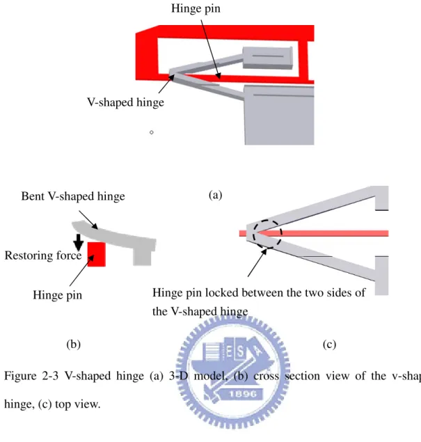
2-1-1 V-shaped hinge...21
2-1-2 Improvement and extension of previous work...21
2-2 Device design...22
2-2-1 Batch assembly ...22
2-2-2 V-shaped hinge...23
2-2-3 Side latch...24
2-2-4 Corner cube reflector ...25
2-2-5 45° mirror design ...26
2-2-6 135° mirror design ...30
2-3 Summary...31
Chapter 3 Fabrication Process...32
3-1 Process flow ...32
3-1-1 Device 1 ...33
3-1-2 Device 2 ...44
3-2-1 Structure patterning...47
3-2-2 Oxide etching...48
3-2-3 Vapor HF release...48
3-3 Summary...51
Chapter 4 Measurement and Results...52
4-1 Batch assembly ...52
4-1-1 Problems ...54
4-2 Reflective coating ...55
4-3 V-shaped hinge...57
4-3-1 Strength of the V-shaped hinge ...59
4-4 Angular accuracy of 90° mirrors...60
4-5 Corner cube reflector ...63
4-5-1 Optical measurement ...65
4-6 45° structures ...68
4-6-1 Device 1 ...68
4-6-2 Device 2 ...71
4-7 Summary...78
Chapter 5 Conclusion and Future work...79
5-1 Conclusion ...79
5-2 Future work...79
List of Figures ______
Figure 1-1 Examples of optical MEMS applications, (a) on-chip optical-disk pickup head system ,, (b) microlens scanner with integrated polymer microlens
[5], (c) optical cross-connect switches [6]. ...2
Figure 1-2 (a) Cross section view of fabrication processes, (b) SEM figure of a hinged structure [8]...4
Figure 1-3 (a) Cross section view of the improved hinge, (b) SEM figure [9]...5
Figure 1-4 (a) Cross section view of a SDA, (b) working principle of SDA [10]...6
Figure 1-5 (a) SEM of a free-rotating hinged micromirror lifted by an array of SDA, (b) structure is lifted by SDA [11]. ...6
Figure 1-6 Schematics of electrostatic force assembly by parallel plates, (a) the voltage is off, (b) the voltage is on...7
Figure 1-7 Sequence of assembly, (a) ultrasonic vibrations heat and charge the ...7
Figure 1-8 (a) Magnetic force assembly, (b) SEM of an assembled structure [14]. ...8
Figure 1-9 Sequence of magnetic force assembly [14]...9
Figure 1-10 Principle of the polyimide V-groove joint [16]...10
Figure 1-11 Large bending by connecting a series of V-grooves [16]...10
Figure 1-12 (a) Fabrication process for surface tension assembly, (b) self-assembled mirror by surface tension [17]...11
Figure 1-13 (a) Schematic of the structures, (b) assembled structure by combining bimorph beams with locking mechanism [19]...12
Figure 1-14 Conventional assembly process. ...13
Figure 1-15 (a) Microgripper is attached to substrate by tethers, (b) metal tip bonded to solder pad [21]. ...14 Figure 1-16 (a) Solder bonded metal tip is attached to the pad, (b) the micro-part is
Figure 1-17 SEM of (a) assembled out-of-plane structures, (b) microcoil [21]. ...15
Figure 1-18 Comparison between (a) conventional beam and (b) serpentine spring [22]...16
Figure 1-19 Assembly procedure (a) no actuation force, (b) the bottom of the device touches the substrate, (c)(d)(e) the conceptual force diagram when the probe moves in lateral direction, (f) finally the structure is at upright position [22]. ...16
Figure 1-20 (a) Optical microscope view of assembly process, (b) SEM image [22]. 17 Figure 2-1 (a) 3-D model, (b) layout design for one-push method [7]...20
Figure 2-2 Assembly process of one-push method [7]. ...20
Figure 2-3 V-shaped hinge (a) 3-D model, (b) cross section view of the v-shaped hinge, (c) top view...22
Figure 2-4 (a) Array of microprobes, (b) schematic of batch assembly...23
Figure 2-5 (a) Conventional hinge, (b) V-shaped hinge. ...23
Figure 2-6 Locking height of the side latches...24
Figure 2-7 Different locking angles of the side latches. ...25
Figure 2-8 (a) Illustration of a corner cube reflector, (b) 3D schematic. ...25
Figure 2-9 (a) Layout design of Device 1, (b) 3-D solid model. ...26
Figure 2-10 Assembly procedure of the device 1 with only one-push operation. ...27
Figure 2-11 (a) Layout design of device 2, (b) 3-D model. ...28
Figure 2-12 Assembly process of the device 2. ...29
Figure 2-13 Form and dimensions of cross sections...30
Figure 2-14 (a) Illustration of 135° structure, (b) 3D schematic. ...31
Figure 3-1 Fabrication process (Device 1)...33
Figure 3-2 Schematic of the vapor HF release setup. ...44
Figure 3-4 Fabrication process (Device 2)...46
Figure 3-5 (a) Illustration of AZ4620 photoresist as the etching mask, (b) before baking, (c) after baking. ...48
Figure 3-6 (a) Water stains on the chip after vapor HF etching, (b) after baking...50
Figure 3-7 Fabricated devices, (a) 90° device without side latch, (b) close-up view of the V-shaped hinge, (c) corner cube reflectors, (d) 45° device...51
Figure 4-1 Setup for batch assembly...53
Figure 4-2 Sequence of batch assembly of three mirrors, (a) probes are aligned to the push pads, (b) the middle mirror was pushed up first, (c) other mirrors were assembled subsequently, (d) mirrors were assembled at 90°...53
Figure 4-3 Sequence of a failed batch assembly, only two samples were pushed up..55
Figure 4-4 (a) Mirror before coating (b) mirror after coating...56
Figure 4-5 (a) Layout of the conventional hinge, (b) right side, (c) left side. ...57
Figure 4-6 (a) Layout of the V-shaped hinge, (b) SEM photograph of the V-shaped hinge, (c) zoom in of the V-shaped hinge. ...58
Figure 4-7 (a) SEM photograph of 90° mirror without side latch, (b) and (c) the same sample taken at two measurements...59
Figure 4-8 Step in the SU-8 photoresist, (a) layout design (b) cross section, (c) schematic, (d) SEM photograph of the SU-8 step [7]...61
Figure 4-9 Change the SU8-step in layout, (a) layout design, (b) cross section...61
Figure 4-10 Offset of the mirror plate...62
Figure 4-11 Side latches with different flip-up angles, (a) 10°, (b) 20°, (c) 40°. ...63
Figure 4-12 Measured angle of mirrors with different side latches angles...63
Figure 4-13 (a) Assembled corner cube reflector, (b) surfaces of the corner cube reflector. ...64
Figure 4-15 Illustration of the optical measurement...65
Figure 4-16 (a) Experimental setup, (b) highlight of the corner cube reflector...65
Figure 4-17 Optical path alignment, (a) laser beam alignment, (b) lens and beam splitter alignment. ...66
Figure 4-18 Reflected spots on the screen placed at (a) 10 mm, (b) 60 mm away from the beam splitter. ...67
Figure 4-19 Angular deviation of the corner cube reflector...67
Figure 4-20 Fabricated Device 1, (a) 45° structure, (b) support of 45° structure (b) 135° structure, (d) support of 135° structure. ...68
Figure 4-21 Mechanical steps in SU-8, (a) 45° device, (b) 135° device. ...69
Figure 4-22 Cross sectional view, (a) After SU-8 process. (b) problem of the assembly process...70
Figure 4-23 SEM of 135° devices, (a) restoring force beam was destroyed due to the step, (b) the step lock the structure out of rotational axis. ...70
Figure 4-24 Assembly process of a 45° mirror without SU-8, (a) before assembly, (b) the mirror was first aligned and pushed up by Probe 1...71
Figure 4-25 (a) An assembled 45° device, (b) side view of 45° device, (c) Highlight of the locking mechanism, (d) torsional beam and mechanical stop (continued). ...73
Figure 4-26 An assembled mirror at 45.8°...74
Figure 4-27 The bent supports, (a) side view, (b) perspective view. ...75
Figure 4-28 Bending of the supports after assembly, (a) 3-D profile. ...75
Figure 4-29 (a) Simulation of the support, (b) side view...76
Figure 4-30 (a) Simulation of a thicker support, (b) side view...76
Figure 4-31 Broken torsional beam. ...77
List of Tables _____
Table 3-1 Parameters of vapor HF release...43
Table 3-2 Modified parameters of vapor HF release ...49
Table 4-1 Different rotation angles of the corner cube reflector...67
Chapter 1
Introduction
1-1
Motivation
Micro Electro-Mechanical Systems (MEMS) is a technique to fabricate mechanical structures at microscales. Mechanical structures, actuators, sensors, and optical elements in MEMS can be implemented by bulk micromachining [1], surface micromachining [2], and the LIGA processes [3]. Bulk micromachining fabricates micro-components by anisotropic or isotropic etching of the substrate which usually is silicon. Surface micromachining is the planar process by deposition and etching of substrate and sacrificial layers to fabricate mechanical structures. High planar resolution is the advantage of surface micromachining which is the most widely used technique to fabricate microstructures. The LIGA process is suitable for manufacturing structures with high aspect ratio (i.e., structures that are much higher than broad).
In the past years, MEMS techniques have been applied to optical engineering, and biomedical engineering. In particular, three-dimensional (3-D) out-of-plane structures on the silicon wafers are important components in applications such as free-space optical bench [4]. Figure 1-1 shows the scanning electron micrographs (SEM) of an optical pickup head and other 3-D applications [4-6]. Furthermore, many sensors and actuators also have the demand for 3-D structures. Batch fabrication and assembly processes are important issues for MEMS technique with new 3-D applications. Many techniques for fabricating complex 3-D structure have been proposed in the past 20 years. One of the most important issues for the 3-D structures is angular positioning of out-of-plane structures, especially for optical applications. Based on this demand, a micro assembly process with good positioning accuracy is needed for fabricating an
optical bench. In our previous study [7], 90° out-of-plane structures were fabricated and assembled by the proposed one-push method. However, the angular accuracy still needs to be improved and an assembly method for arbitrary angles is also desired. Thus, solving the angular accuracy problem and developing the assembly method for arbitrary angles are the objectives of this thesis.
Figure 1-1 Examples of optical MEMS applications, (a) on-chip optical-disk pickup head system ,, (b) microlens scanner with integrated polymer microlens [5], (c) optical cross-connect switches [6].
(a)
Micro-Fresnel lens
Beam-splitter 45o reflector
1-2
Literature survey
Most 3-D components are fabricated by surface micromaching and then flipped up to form the 3-D microstructures. Micro hinges are a common solution to anchor the flip-up components. In the past years, many assembly methods for 3-D structures have been proposed. In addition to manual assembly, external forces powered by scratch drive actuators, magnetic force, electrostatic force, or ultrasonic agitation were also used to assemble 3-D structures. Pre-stressed bimorph beams and surface tension were also used for self-assembly. Recently, automatic assembly process was also demonstrated by standard or specially designed equipments. In this section, techniques for 3-D structure assembly are reviewed.
1-2-1 Microfabricated hinges
Surface micromachining is usually used to manufacture MEMS devices with the structure layer thickness less than 5µm. It was developed in the 80's for combining MEMS and planar integrated circuits (IC) technology on a common silicon wafer. In [8], the proposed micro hinge structures enabled the surface micromachined structures to rotate out of the plane. Two structural layers were used to fabricate the hinge. The poly-1 layer was used as structure layer and hinge pin, while the poly-2 layer was used to fabricate the hinge staple that could cover the hinge pin, as shown in Figure 1-2. This invention enabled micro-structures to rotate out of the plane and also opens an important door for future three-dimensional (3-D) applications.
Figure 1-2 (a) Cross section view of fabrication processes, (b) SEM figure of a hinged structure [8].
However, conventional microfabricated hinges have an important problem due to the play between the pin and the staple. Therefore the pin can not be precisely positioned. In order to solve this problem, an improved hinge was proposed [9], as shown in Figure 1-3. A cantilever beam was used to press and fix the hinge pin, which was made wider than the polysilicon layer thickness. The vertical hinge play was eliminated in this invention and the fabricated structure could not shift vertically anymore. However, the lateral play still existed and would cause shift in assembly process.
To eliminate the lateral play and improve the positioning accuracy, a solution was proposed in our previous study [7]. The V-shaped hinge locks the hinge pin in desired axis by the geometric design. The comparison between the V-shaped hinge and the conventional hinge will be presented in Chapter 4.
PSG PSG Silicon Poly-1 Poly-2 Plate Hinge pin (a) (b)
Figure 1-3 (a) Cross section view of the improved hinge, (b) SEM figure [9].
1-2-2 Three dimensional MEMS by powered assembly
Assembly powered external forces such as scratch drive actuators, magnetic force, electrostatic force, and ultrasonic agitation are reviewed in this section.
Scratch drive actuator assembly
The scratch drive actuator (SDA), as shown in Figure 1-4, was proposed in 1993 [10]. A scratch drive actuator is usually composed of a plate, a bushing, an insulator and a substrate electrode, as shown in Figure 1-4 (a). With an applied voltage, the plate is pulled down to the substrate by the electrostatic force. The bushing is tilted at this stage and moves a small distance. Once the voltage is removed, the plate and bushing return to their initial position. With this motion in cycles, the SDA can go forward to the desired position. Figure 1-4 (b) shows the working principle step by step. Figure 1-5 illustrates a micromirror assembled by using an array of SDA [11].
cantilever anchor
slider
pin (rotated 90o) slider
cantilever
(a) (b)
Figure 1-4 (a) Cross section view of a SDA, (b) working principle of SDA [10].
Figure 1-5 (a) SEM of a free-rotating hinged micromirror lifted by an array of SDA, (b) structure is lifted by SDA [11].
Electrostatic force assembly
Electrostatic force generated by parallel plates [12] or ultrasonic waves [13] can be used to assemble 3-D structures. The operation principle of generating electrostatic force by parallel plates is shown in Figure 1-6. When the voltage is applied, the electrostatic attraction force between the ground plane and the hinged plate enables the hinged plate to move out of the plane, as shown in Figure 1-6 (b). The advantage of electrostatic force assembly is easy control of voltage.
Push bar SDA Force Mirror Rotated hinge Plate Bushing Insulator Substrate (a) (b) (a) (b)
In addition to parallel plates, ultrasonic wave is another way to generate electrostatic force. Ultrasonic vibrations are generated with an attached piezoelectric actuator to vibrate polysilicon plates on silicon nitride or polysilicon surfaces [13]. The friction brings contact electrification charge on the substrate and the flap. The electrostatic repulsion force is generated to lift up the flap, as Figure 1-7 shows. The parts were first actuated in ambient pressure (Figure 1-7(a)). However, at atmospheric pressure the structures would not be lifted up due to the air drag on the flaps. As the pressure was low enough with the ultrasound still on, the hinged flaps were lifted up (Figure 1-7(b)).
(a) (b)
Figure 1-6 Schematics of electrostatic force assembly by parallel plates, (a) the voltage is off, (b) the voltage is on.
In air with ultrasound In vacuum with ultrasound (a) (b)
Figure 1-7 Sequence of assembly, (a) ultrasonic vibrations heat and charge the polysilicon parts, (b) electrostatic repulsion forces the plate up [13].
Surface charge raises the flap Flap is vibrating
Surface friction generates charges
PZT plate Silicon substrate
V Off V On
Ground plane
Substrate
Hinged plate Electrostatic
Magnetic force assembly
Magnetic forces can be applied to actuate assemble 3-D structures by passing current through them (Lorentz force) or by depositing magnetic material on them. As shown in Figure 1-8 (a), electroplated magnetic material such as Permalloy is integrated with the hinged flap [14]. When an external magnetic field is applied, the hinged flap will be lifted up and rotate around the rotational axis. The rotation angle is determined from the volume of the magnetic material and the applied external field. Figure 1-8 (b) shows an assembled structure by the magnetic force. By choosing different volume of Permollay electroplated on the flap, a precise sequence assembly can be achieved by changing the magnetic field strength [14, 15]. An example is shown in Figure 1-9. As Hext is increased gradually, the primary flap will be lifted up to 90° first due to the greater volume of Permolloy. With the increase of Hext, the secondary flap will be lifted up and lock the primary flap by the friction force.
(a) (b)
Figure 1-8 (a) Magnetic force assembly, (b) SEM of an assembled structure [14]. Hext
Hinge
Flap Magnetic material
Figure 1-9 Sequence of magnetic force assembly [14].
1-2-3 Three dimensional MEMS by self assembly
Aside from external applied forces, 3-D microstructures can be assembled by the intrinsic force of the fabricated structures. In other words, the fabricated structure can be assembled to 3-D structure itself. Self assembly by pre-stressed bimorph beams, surface tension, and thermal shrinkage of polyimide in V-grooves are reviewed in this section.
Self assembly by thermal shrinkage of polyimide in V-grooves
Thermal shrinkage of polyimide in V-grooves can be used for self assembly as illustrated in Figure 1-10 [16]. V-grooves are etched through a silicon membrane and filled with polyimide. The polyimide in V-grooves shrinks when it is cured. With a lager lateral length of polyimide at the top of the V-groove than at the bottom, the structure bends as a result of to different amount of shrinkage of polyimide. With a series of V-grooves, large bending can be achieved, as shown in Figure 1-11 [16].
Primary flap
Secondary flap
(a) (b) Figure 1-10 Principle of the polyimide V-groove joint [16].
Figure 1-11 Large bending by connecting a series of V-grooves [16].
Surface tension powered self assembly
In surface tension powered self assembly [17], meltable material is patterned on the hinge joint. The plate is flipped up by surface tension when the material is melted. The fabrication process and a fabricated structure are shown in Figure 1-12. The rotation angle of the assembled structures are determined by the geometric features of the meltable material [18].
(a) (b)
Figure 1-12 (a) Fabrication process for surface tension assembly, (b) self-assembled mirror by surface tension [17].
Stress-induced self assembly
Residual stress of thin film can be used as motive force to assemble 3-D microstructure, as Figure 1-13 shows [19]. The assembly mechanism is composed of stress-induced bimorph beams and locking components. The locking mechanism fabricated in different structure layers is engaged when the micromirror is raised.
Bimorph stress beams can be fabricated by using different materials. However, the stress relaxation is a critical problem. Reliability tests showed that the problem of stress relaxation could be reduced by replacing metal films by dielectric films [20].
photoresist Spin resist Pattern and Premelt resist Release Flap
Figure 1-13 (a) Schematic of the structures, (b) assembled structure by combining bimorph beams with locking mechanism [19].
1-2-4 Manual or robotic assembly
Microprobes are the first tool for manual assembly of fabricated micro parts. It is time consuming and has low yields. In recent years, specially designed robotic equipments are also developed for automatic assembly. These assembly techniques are reviewed in this section.
Conventional manual assembly
The conventional manual assembly of a flip-up mirror is illustrated in Figure 1-14. The structure is composed of a mirror plate, two mechanical locks, and a number of hinges. First a microprobe is used to lift up the micromirror to be perpendicular to the substrate. Then the mechanical side locks are picked up by another microprobe while the micromirror is held by the original microprobe. Finally the side locks are folded and locked onto the plate by the V-shaped opening. Precise manipulation of microprobes is needed during the assembly process in this conventional manual assembly. Stress beam Micromirror Locking mechanism Stress beam Tapered cut Hinged sidewall Dovetail Frame
Figure 1-14 Conventional assembly process.
Assembly by microgrippers
Compliant passive microgrippers were proposed to assemble out-of-plane 3-D microstructures [21]. The surface-micromachined microgripper is originally attached to the substrate by tethers, which are weak enough to be pulled apart from the substrate. Figure 1-15 shows the surface micromachined microgripper and the solder bonded microgripper. First, the solder is melt by the heated metal tip which is attached to a robotic arm. Then the metal tip with melt solder on it is aligned and pressed on the solder pad of the microgripper. After cooling, the pad is bonded to the metal tip. The tethers can be easily broken when the arm moves away from the substrate (Figure 1-16 (a)). Next, the microgripper is aligned to the micromachined microparts. The microgripper is inserted into the microparts (Figure 1-16 (b)). After inserting the microparts into the slots on the substrate, the microgripper is released and the assembly is complete (Figure 1-16 (c)). Figure 1-17 shows the SEM figures of the assembled devices.
Micromirror
Side locks
Microprobe
Figure 1-15 (a) Microgripper is attached to substrate by tethers, (b) metal tip bonded to solder pad [21].
Figure 1-16 (a) Solder bonded metal tip is attached to the pad, (b) the micro-part is grasped by the microgripper, (c) the micro-part is inserted in the slot [21].
(a) (b)
(c)
Figure 1-17 SEM of (a) assembled out-of-plane structures, (b) microcoil [21].
Hingeless 90° out-of-plane microstructures
Another novel technique for microassembly is the assembly of hingeless 90° out-of-plane microstructures with the use of automated probing system [22]. Staple hinges are replaced by compliant hinges created using springs or torsion beams, which can produce out-of-plane motion by redirecting lateral displacement into rotation. The structure can be pushed up by a single lateral push. While the conventional springs are complaint in all direction, the serpentine springs are designed to be more compliant in the out-of-plane direction than the in-plane direction, as shown in Figure 1-18. When a lateral force is applied on the actuation pad, the spring is twisted and a 90° out-of-plane motion can be produced. The assembly process is presented in Figure 1-19. The lateral actuation force (FA) and the restoring force of the springs (FS) provides an out-of-plane torque after the bottom of the device touches the substrate (Figure 1-19(b)). As the probe moves in lateral direction, the rotational torque (which is associated to FS) increases because of the deformation of the springs (Figure 1-19(c)(d)). When the plate reaches a particular angle, the spring will begin to
pull the plate until the structure finally reaches the upright position (Figure 1-19(e)(f)). Figure 1-20 (a) shows the manual assembly procedure. Figure 1-20 (b) is an assembled device.
Figure 1-18 Comparison between (a) conventional beam and (b) serpentine spring [22].
Figure 1-19 Assembly procedure (a) no actuation force, (b) the bottom of the device touches the substrate, (c)(d)(e) the conceptual force diagram when the probe moves in lateral direction, (f) finally the structure is at upright position [22].
Effective axis of rotation
Rotational compliance (out of plane) Point of actuation
Point of actuation Axis rotation
Compliant in all direction
(a) (b)
(c) (d) (e) (f)
Anchor Anchor
(a)
Figure 1-20 (a) Optical microscope view of assembly process, (b) SEM image [22].
1-2-5 Conclusion
Although there are a number of methods for 3-D microstructure assembly, the applications of these methods are limited. Assembly by SDA needs large chip area. Assembly by magnetic or electrostatic force needs materials which are not compatible with IC processes or demands a large electrical field. Parameters of thermal shrinkage of polyimide or surface tension forces are difficult to control. Bimorph stress beams have the problem of stress relaxation. Manual assembly by micromanipulators is time consuming. However, once the steps of manual assembly are simplified enough and automatic equipments can be used, systematic assembly can be achieved.
(a) (b)
(i) (ii)
1-3
Objective and organization of the thesis
In our previous [7], a novel assembly method with one-push operation was proposed to lift up 3-D microstructures. SU-8 was used to fabricate locking mechanism. A novel hinge design was also introduced to improve the positioning accuracy.
Batch assembly in wafer level will be demonstrated in this thesis. The accuracy problem that was found in [7] will be solved. A corner cube reflector is demonstrated based on this method. Furthermore, 45° positioning method needed for optical benches will be introduced. Therefore, the objectives of this thesis are to:
1. demonstrate batch assembly;
2. verify the hinge positioning accuracy; 3. solve the angular accuracy problem;
4. apply the method to a corner cube reflector;
5. demonstrate the assembly method for arbitrary angles.
The basic principles and simulation of the proposed microstructures and assembly method are presented in Chapter 2. The fabrication processes and process issues are discussed in Chapter 3. The experiment and measurement results of the fabricated and assembled devices are showed in Chapter 4. Conclusion and future work are presented in Chapter 5.
Chapter 2
Principle and Design
The major difficulty in the manual assembly of out-of-plane structures is the precise control of microprobes. First, the microprobe must be inserted into the gaps between the released structure and the substrate. Then the microprobe is maneuvered in different directions with precise position control to lift up the microstructure. In our previous study [7], the operation of the probe is simplified to a single push in the proposed one-push method. The advantage of the proposed method is the large probe positioning tolerance in both vertical and lateral directions.
The proposed method was verified in a SOI/SU-8 process developed in our laboratory [23]. The major advantage of the SOI wafer is the better surface smoothness of the single-crystal-silicon (SCS) device layer compared to the surface micromachined polysilicon layer. This is especially important in optical demands. The SU-8 photoresist is used as the second structural layer. The low temperature process is more compatible with circuits than the polysilicon process. Furthermore, the Young’s modulus of SU-8 is smaller than silicon [24, 25]. Therefore SU-8 is suitable to fabricate springs or restoring force components.
2-1
One-push assembly process
The concept of the proposed one-push operation is shown in Figure 2-1. In Figure 2-1 (a), the substrate is the 400-µm-thick handle layer of the SOI wafer. The micromirror is defined in the 5-µm-thick device layer, whereas the locking mechanisms are fabricated using SU-8 photoresist. The through-wafer hole provides the operation space for the probes during the assembly procedure. The assembly process is shown in Figure 2-2. When a probe pushes the pad down through the
through-wafer hole, the mirror is flipped up and contacts the bottom of the side latches made of the SU-8 photoresist (Figure 2-2 (a)). The out-of-plane force from the mirror plate will simultaneously drive the flexible side latches to rotate out of the plane (Figure 2-2 (b)). When the mirror plate rotates close to 90°, it will slide into the V-shaped slot of the flexible side latches (Figure 2-2(c)). The V-shaped slot and the downward restoring force of the side-latch spring will firmly lock the mirror plate in place after the probe moves away (Figure 2-2 (d)). The manual assembly process is reduced to a single push motion.
Figure 2-1 (a) 3-D model, (b) layout design for one-push method [7].
Figure 2-2 Assembly process of one-push method [7]. Mirror plate
V-shaped hinges Side latches (locking mechanism)
Through-wafer hole Push pad
(a) (b)
(a) (b)
Side latch is lifted up by the mirror Microprobe
Figure 2-2 Assembly process of one-push method [7] (continued).
2-1-1 V-shaped hinge
3-D mirrors are usually fixed to the substrate by staple hinges. For conventional hinges, play space in the staple is needed for the hinge pins to rotate. However, the play can cause an offset of the pin position during assembly that will affect the final angular accuracy. In our previous study [7], a novel V-shaped hinge with less hinge play was proposed, as shown in Figure 2-3. The restoring force of the V-shaped beams eliminates the vertical play and fixes the hinge pin on the substrate. Furthermore, the hinge pin is locked by the geometry of the V-shaped hinge when the mirror is in the upright position, as shown in Figure 2-3(c). Therefore, the offset of the hinge pins due to the transverse play during assembly can be reduced.
2-1-2 Improvement and extension of previous work
In our previous demonstration [7], the average angle of the assembled 90° micromirrors was 89.2±0.3º. The cause and solution of this problem are investigated in this thesis. In this thesis, the batch assembly of more than one device will be demonstrated to reduce the assembly time on the wafer level. Finally, V-shaped hinges are used to fix the position of the flip-up structures without conventional hinges or side latches.
(c) (d)
Standing mirror V-shaped slot
Figure 2-3 V-shaped hinge (a) 3-D model, (b) cross section view of the v-shaped hinge, (c) top view.
2-2
Device design
Batch assembly is realized by three mirrors and an array of microprobes. Several side latches for 90° structures are designed to investigate the offsets on the angular accuracy. A corner cube reflector is designed as another application of the one push assembly method. Mechanisms for 45° and 135° device assembly are proposed and designed.
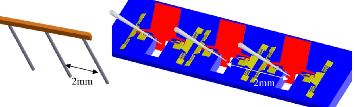
2-2-1 Batch assembly
The schematic of batch assembly is shown in Figure 2-4. An array of microprobes (a)
V-shaped hinge
Hinge pin
(b) (c)
Restoring force
Bent V-shaped hinge
Hinge pin Hinge pin locked between the two sides of
are connected to a micropositioner to push an array of the micromirrors simultaneously. The distance of the microprobes is the same as the distance of the push pads, which is 2 mm. The sizes of the mirror plate and the push pad are (760 µm)2 and (250 µm)2, respectively.
Figure 2-4 (a) Array of microprobes, (b) schematic of batch assembly.
2-2-2 V-shaped hinge
Axis positioning accuracy is compared between a V-shaped hinge and a conventional hinge, as shown in Figure 2-5. The V-shaped hinge in Figure 2-5 (b) is the same as in [7]. The axis offsets of the two designs will be measured and discussed in Chapter 4. The width of the hinge pin of the V-shaped hinge is 15 µm and the deposited oxide is 3 µm thick. A mirror without side latch is also designed to test the robustness of the V-shaped hinge.
Figure 2-5 (a) Conventional hinge, (b) V-shaped hinge.
2mm 2mm
(a) (b)
2-2-3 Side latch
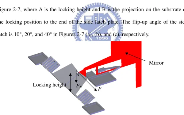
Side latches are used to lock the side plates of the mirror plates. The locking height affects the robustness of the assembled structure. For lower locking height, the same offset at locking point should result in greater angular deviation. However, the friction force between the silicon and the SU-8 photoresist affects the locking position. As Equation 2-1 shows, F is the friction force,
µ
is the coefficient of friction, and FNis the normal force exerted on the surfaces. A larger flip-up angle of the side latch will result in a large FN due to the increased restoring force from the spring (Figure 2-6).
N
F =
µ
⋅F (2-1)The side latch spring is designed to be rigid in the out-of-plane direction in order to lock the mirror plate. The geometric design of three locking angles is shown in Figure 2-7, where A is the locking height and B is the projection on the substrate of the locking position to the end of the side latch plate. The flip-up angle of the side latch is 10°, 20°, and 40° in Figures 2-7 (a), (b), and (c), respectively.
Figure 2-6 Locking height of the side latches.
Mirror
F FN
(a) A=38 µm, B=216.5 µm 1 38 o tan 10 216.5 θ − = = (b) A=56µm, B=154µm 1 56 o tan 20 154 θ − = = (c) A=113µm, B=135µm 1113 o tan 40 135 θ − = =
Figure 2-7 Different locking angles of the side latches.
2-2-4 Corner cube reflector
The corner cube reflector is composed of two 90° mirrors, as shown in Figure 2-8. The three reflecting surfaces are the front side of Mirror 1, back side of Mirror 2, and the surface of substrate underneath Mirror 2, as shown in Figure 2-8 (b). The reflecting zone is (760 µm)3.
Figure 2-8 (a) Illustration of a corner cube reflector, (b) 3D schematic.
A B A B A B Mirror 1 Mirror 2 760µm 760µm Through-wafer hole (a) (b) Mirror 1
Out of plane rotation
Push pad
2-2-5 45° mirror design
In this section, two 45° structures are proposed. The difference between the two devices is that Device 1 utilizes SU-8 as the supporting structures and restoring force beams for the 45° SCS device, whereas Device 2 only utilizes the SCS layer on the SOI wafer to fabricate the structures.
2-2-5-1 Device 1
As shown in Figure 2-9, the 45° mirror consists of a mirror plate, V-shaped hinges, restoring force beams, and side supports. The mirror structure is in the SCS layer of the SOI wafer and the side supports are made of SU-8 photoresist. The rectangular SU-8 is attached to the side supports instead of the mirror plate.
(a) (b) Figure 2-9 (a) Layout design of Device 1, (b) 3-D solid model.
The assembly procedure of device 1 is shown in Figure 2-10. First the microprobe is aligned to the push pad (Figure 2-10 (a)). Once the mirror rotates out of the plane when the probe pushes the pad, the mirror plate contacts the SU-8 layer. Then the
Mirror plate
Restoring force beam
V-shaped hinge Side supports
Through-wafer hole Locking mechanism Rectangular SU-8
rectangular SU-8 attached on the side supports are pushed upward due to the upward force from the main mirror structure (Figure 2-10 (b)). As the side supports are pulled to 90°, it is locked at 90° by the side latches (Figure 2-10 (c)). Once the probe is removed, the mirror plate will lie back on the side supports due to the restoring force beams and fixed by the designed latches (Figure 2-10 (d)).
Figure 2-10 Assembly procedure of the device 1 with only one-push operation.
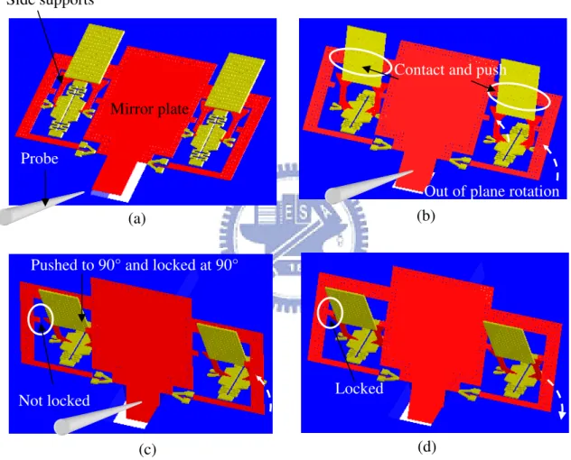
2-2-5-2 Device 2
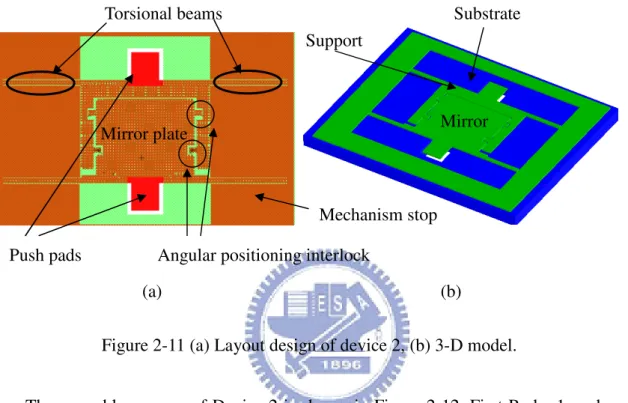
In consideration of the complex structures in Device 1, Device 2 is designed without SU-8, but with only the SCS layer. However, two microprobes are needs in the push operation for this design. In Figure 2-11, the mirror and the support are in the
(a) (b)
(c) (d)
Contact and push
Side supports
Mirror plate
Pushed to 90° and locked at 90°
Not locked Locked Probe
device layer of the SOI wafer, whereas the substrate provides the space for pushing. The layout and 3-D solid model are shown in Figure 2-10. Compared to Device 1, this design has a simplified structure. The mirror plate is (760 µm)2. The length of the support beam is 800 µm and the width is 120 µm.
(a) (b)
Figure 2-11 (a) Layout design of device 2, (b) 3-D model.
The assembly process of Device 2 is shown in Figure 2-12. First Probe 1 pushes the support to over 65° (Figure 2-12 (a)). Then Probe 2 pushes the mirror plate to 45°~55° with Probe 1 held in position (Figure 2-12 (b)). Subsequently Probe 1 is removed and the torque from the torsinal beams drives the support to lie on the mirror plate (Figure 2-12 (c)). After Probe 2 is removed, the downward force of the mirror plate also drives the mirror plate to lie on the support. Finally, the support and the mirror plate are interlocked (Figure 2-12 (d)).
Torsional beams
The torsional beams are used to provide restoring force. The design of the torsional beams is similar to [26]. For a 45° mirror, the twist angle of the torsional
Mirror plate Torsional beams
Push pads
Mechanism stop Support
Angular positioning interlock
Substrate
beams is 45°. However, during the assembly process the support is needed to be twisted to over 80°. Thus the twist angle of 80° is adopted in this design. The torsional beam design is based on the torsion formula of a beam with a rectangular cross section [27], L KG θ = Γ , (2-2) 4 3 4 16 [ 3.36 (1 )] 3 12 b b K ab a a = − − , (2-3) 2 3 4 max 3 3 [1 0.6095 0.8865( ) 1.8023( ) 0.9100( ) ], for a b 8 b b b b ab a a a a τ = Γ + + − + ≥ , (2-4)
where θ is the angle of twist, Γ is twisting moment, L is beam length, K is a constant depending on the geometry of beam, G is shear modulus, τmax is the maximum shear stress at the midpoint of the longer side compared between a and b, a and b is half of the longer and shorter sides of the cross section of the beam, respectively (Figure 2-13).
Figure 2-12 Assembly process of the device 2.
(a) (b)
(c) (d)
Probe 1
Probe 2
Figure 2-13 Form and dimensions of cross sections.
The device layer of the SOI wafer is 5 µm and therefore a is 2.5µm. The width of the beam is 45 µm and therefore b is 22.5 µm. The shear modulus of single-crystal silicon is 79.9 GPa [28] and the yield strength of single-crystal silicon is 7 GPa [26]. The maximum shear stress (τmax) in this structure when θ=80° must be smaller than the yield strength and τmax = 5 GPa is used in the design. By substituting these values into Equations 2-2, 2-3, and 2-4, K and Γ are 1.74×10⁻²¹ m4 and 1.74×10⁻⁶ N.m, respectively. From the Equation 2-2, L is equal to 112 µm.
2-2-6 135° mirror design
The 135° mirror is constructed by a mirror plate, four restoring force beams, and two 90° supports, as shown in Figure 2-14. The fabrication process of the 135° structure is the same as Device 1 in the 45° design. Two push operations are needed in the assembly process. The 90° supports, which are similar to the 90° mirrors in [7], are first pushed up. Then the mirror plate is pushed to 135° and fixed on the two 90° supports by the downward force from the restoring force beams, as shown in Figure 2-14 (b).
2b 2a L
(a) (b)
Figure 2-14 (a) Illustration of 135° structure, (b) 3D schematic.
2-3
Summary
Three mirrors and an array of microprobes are designed to demonstrate the batch assembly. Different locking angles of the side latches are used to test the positioning angular accuracy. Two 90° mirrors are used to construct a corner cube reflector. The 45° and 135° structures and their locking mechanisms are designed for its feasibility. In Chapter 3, the fabrication is discussed.
Mirror
Support (90° mirror) Anchor
SU-8 restoring force beam
Hinge
Chapter 3
Fabrication Process
In this chapter, a surface micromachining-like fabrication process is described. The SU-8 photoresist is used with silicon-on-insulator (SOI) wafers to simplify the process flow. The SOI wafer is chosen with its flat surface characteristic of single crystal silicon. Using SOI wafers can also reduce the complexity of the process. SU-8 photoresist is used as a structure layer. Compared to the use of polysilicon as the structure layer, SU-8 photoresist can reduce the process complexity. Another advantage of using SU-8 is that the process temperature is low, which is more compatible with IC processes. However, the Young’s modulus of SU-8 is about 4 GPa, while that of polysilicon is about 160 GPa. Therefore the deformation of SU-8 is larger than polysilicon under the same stress. Therefore, SU-8 structures should be well designed for angular positioning, as discussed in Chapter 2. The process of integration of SOI wafer with SU-8 photoresist is described in the following. The fabrication parameters are listed and some issues are discussed.
3-1
Process flow
As described in Chapter 2, SU-8 photoresist is used as a structure layer for angular positioning in Device 1. Therefore, the fabrication process includes both SOI wafers and SU-8 photoresist. In contract to Device 1, the device layer of the SOI wafer is used for angular positioning in Device 2. Consequently, the fabrication process is simpler in Device 2 without using SU-8 photoresist.
SOI Substrate
Single crystal silicon layer
Buried oxide
SOI Substrate SOI Substrate Buried oxide
3-1-1 Device 1
The fabrication process of Device 1 is shown in Figure 3-1. The device was fabricated in the Nano Facility Center at National Chiao Tung University. The SOI wafers have a device layer of 5 µm, buried oxide layer of 2 µm, and handle layer of 400 µm.
(a) RCA cleaning (Step A)
(b) Front side patterning (Step B, Step C)
(c) Backside oxide deposition (Step D)
Figure 3-1 Fabrication process (Device 1).
SOI Substrate Buried oxide SOI Substrate SOI Substrate SOI Substrate Buried oxide
(d) Anchor definition (Step E, Step F)
(e) Oxide deposition, anchor patterning (Step G, Step H, Step I)
(f) Backside oxide definition (Step J, Step K)
(g) SU-8 coating (Step L)
Figure 3-1 Fabrication process (Device 1) (continued). PECVD Oxide
Buried oxide PECVD Oxide
Buried oxide PECVD Oxide AZ4620 photoresist
PECVD Oxide SU-8 photoresist
Buried oxide
(h) Backside ICP etching (Step N)
(i) Oxide release (Step O)
(j) Push (Step P)
Figure 3-1 Fabrication process (Device 1) (continued).
Step A: RCA cleaning
A standard RCA clean process was first performed on the bare SOI wafer. The process will remove the organic contaminants, the native oxide layer, and the ionic
PECVD Oxide SU-8 photoresist
SOI Substrate SU-8 photoresist
contaminants. Detailed parameters are shown below. In consideration of the buried oxide in the SOI wafer, the chemical oxide removal process is reduced to 30 seconds. Between each step is de-ionized water rinse.
Step B: Photolithography – Device layer definition (Mask1)
The FH6400 positive photoreisit is coated on the SOI wafer as the etching mask for defining the device layer by inductively coupled plasma (ICP). Mask 1 defines the main structure on the 5-µm-thick device layer. Detailed parameters are listed as below
Step Description Parameters
0 Photoresist FH6400
1 HMDS coating Vapor prime oven
Coating (spread cycle) 1000 rpm 10 sec
2
Coating (spin cycle) 2000 rpm 35 sec
3 Soft bake 90° C hotplate 150 sec
4 Exposure Karl Suss MJB-3 mask aligner (3.2 mW/cm
2) for 90 sec
5 Development Developer FHD-5 for 55 sec
6 Rinse D.I. water 1 min
7 Hard bake 120° C hotplate 30 min
Step C: Inductively coupled plasma silicon etching
Inductively coupled plasma (ICP) is used to etch the 5-µm-thick silicon device
Step Parameters
0 D. I. water Rinse (5 min)
1 H2SO4 : H2O2 = 3 : 1 (10~15 min, 75° C ~85 ° C)
2 HF : H2O = 1 :100 (30 sec, room temperature)
3 NH4OH : H2O2 : H2O = 1 : 4 : 20 (10~15 min, 75° C ~85 ° C) 4 HCL : H2O2 : H2O = 1 : 1 : 6 (10~15 min 75° C ~85 ° C)
layer with the mask defined in Step B. This process is performed by the ICP etching service of ITRC (Instrument Technology Research Center) and NTU (National Taiwan University). The parameters of the ICP etching at NTU (STS MESC multiplex ICP) are listed below.
Description Etch phase parameters Passivation phase parameters
Time per cycle 11.5 seconds 7.0 seconds
SF6 flow rate 130 sccm 0 sccm
C4F8 flow rate 0 sccm 85 sccm
O2 flow rate 13 sccm 0 sccm
Coil RF power 600 W 600 W
Platen RF power 11.5 W 0 W
Process pressure APC position = 81.2 % Base pressure = 0.3 mtorr Helium backside
cooling
Helium backside pressure = 10 torr Maximum helium leak up rate = 20 mtorr/min
Etch rate 0.6-0.7 µm per cycle depending on pattern
Step D: Backside silicon oxide deposition
Silicon oxide is deposited by a BR-2000LL plasma enhanced chemical vapor deposition (PECVD) system on the backside of the handle layer. The deposited oxide layer with a thickness of 4.5 µm will be used as a hard mask for 400 µm ICP etching process. The thickness of the oxide layer is determined according to the 1:100 selectivity between the oxide and the silicon in the ICP process.
Description Parameters
SiH4 flow rate 5 sccm
N2O flow rate 90 sccm
Process pressure 400 mTorr
Process temperature 350° C
RF power 11 W
Step E: Photolithography – Anchor definition (Mask 2)
The anchor pattern is defined with Mask 2 in AZ4620 positive photoresist. The 2- µm-thick buried oxide layer of the SOI wafer is then etched by RIE. The selectivity between buried oxide and the AZ4620 photoresist is about 1:2 in the RIE process. Therefore, 5-µm-thick photoresist is coated in this step.
Step Description Parameters
0 Photoresist AZ4620
1 HMDS coating Vapor prime oven
Coating (spread cycle) 1000 rpm 10 sec
2
Coating (spin cycle) 2500 rpm 30 sec
3 Soft bake 90° C hotplate 25 min
4 Exposure Karl Suss MJB-3 mask aligner (3.2 mW/cm
2) for 350 sec
5 Development Developer AZ-300 for 4 min 35 sec
6 Rinse D.I. water 1 min
7 Hard bake 120° C hotplate 60 min
Step F: Polysilicon reactive ion etching (Poly-Si RIE) – Buried oxide etching
The buried oxide layer exposed in Step E is etched by RIE (SAMCO RIE-10N). The 2-µm-thick oxide in the anchor areas is removed in this step to ensure the contact and adhesion between the SU-8 and the silicon.
Description Parameters
SF6 flow rate 30 sccm
CHF3 flow rate 10 sccm
Helium backside cooling about 15 sccm
Process pressure 50 mtorr
RF power 100 W
Step G: Front side silicon oxide deposition
The sacrificial oxide layer between the SU-8 and the silicon device layer of the SOI wafer is deposited on the front side in this step by PECVD. The buried oxide and the silicon oxide deposited in this step provide the hinge pin rotation space after releasing. The deposition thickness is 3 µm.
Description Parameters
SiH4 flow rate 5 sccm
N2O flow rate 90 sccm
Process pressure 400 mTorr
Process temperature 350° C
RF power 11 W
Deposition time Two 23-minuate deposition for 1.5 µm each
Step H: Photolithography – Anchor definition (Mask 3)
Similar to Step E, anchor is defined again in this step. The oxide deposited in the previous step will be etched in the next step with the pattern defined in this step. Since the selectivity between PECVD oxide and AZ4620 photoresist is about 1:1.7 in the RIE process, a 7-µm-thick photoresist of AZ4620 is coated on the wafer.
Step Description Parameters
0 Photoresist AZ4620
1 HMDS coating Vapor prime oven
Coating (spread cycle) 1000 rpm 10 sec
2
Coating (spin cycle) 2000 rpm 30 sec
3 Soft bake 90° C hotplate 28 min
4 Exposure Karl Suss MJB-3 mask aligner (3.2 mW/cm
2) for 350 sec
5 Development Developer AZ-300 for 4 min 35 sec
6 Rinse D.I. water 1 min
Step I: High density plasma reactive ion etching (HDP-RIE) – PECVD oxide etching This step defines the contact between the silicon device layer and the SU-8 layer. About 3-µm-thick oxide deposited by PECVD is etched. To prevent etching of the silicon device layer, HDP-RIE is used for its good selectivity between the silicon and oxide in this step. Thus the 5-µm-thick silicon will not be etched, as marked in Figure 3-1 (e). The prolonged etching time can ensure the complete removal of the oxide on the silicon device layer and silicon substrate.
Description Parameters
Ar flow rate 40 sccm
CHF3 flow rate 40 sccm
Helium backside cooling Open
Process pressure 10 mtorr
ICP RF power 750W
Bias RF power 120 W
Etch rate 1 µm per 500 sec
Step J: Photolithography on backside silicon oxide (Mask 4)
The wafer through hole is defined in this step as the space for pushing. The oxide layer is deposited in Step D. This step patterns the oxide by AZ4620 photoresist. The patterned oxide will be used as the hard mask for etching the 400 µm silicon on the backside of the SOI wafer. An EV620 double side aligner at National Tsing Hua University (NCTU) is used for the photolithography process. About 8 µm photoresist is coated in this step.
Step Description Parameters
0 Photoresist AZ4620
1 HMDS coating Vapor prime oven
Coating (spin cycle) 2000 rpm 40 sec
3 Soft bake 90° C hotplate 27 min
4 Exposure EV620 mask aligner (10 mW/cm2) for 12 sec
5 Development Developer for 1 min 15 sec
6 Rinse D.I. water 1 min
7 Hard bake 120° C hotplate 60 min
Step K: Polysilicon reactive ion etching (Poly-Si RIE) – Backside oxide etching The patterned 4.5 µm oxide is etched in this step. Over etching is also needed to ensure complete removal of the oxide on the silicon. The selectivity between the PECVD oxide and the AZ4620 photoresist is 1:1.8.
Description Parameters
SF6 flow rate 30 sccm
CHF3 flow rate 10 sccm
Helium backside cooling about 15 sccm
Process pressure 50 mtorr
RF power 100 W
Etch rate 18 min for 2 µm PECVD oxide
Step L: SU-8 photolithography (Mask 5) – SU-8 structure layer definition
The 13-µm-thick SU-8 negative photoresist is deposited as a structure layer by Mask 5 in this step. This step is important for angular accuracy of the device. However the aligner used to fabricate the devices has a alignment accuracy of 2 µm, so the accuracy for the final device may be limited.
Step Description Parameters
0 Photoresist SU-8 2010
1 Native oxide remove BOE 10 sec (etching rate: 1000 Å/min)
2 Pre-bake 150° C hotplate 20min
Coating (spin cycle) 3000 rpm 30 sec
4 Pre-exposure bake
25° C to 65° C hotplate, 65° C for 1 min 65° C to 95° C hotplate, 95° C for 2 min
95° C to 25° C, rate: 1° C/min
5 Exposure K-310P-100S mask aligner (35 mW/cm
2) for 4 sec
6 Post-exposure bake
25° C to 65° C hotplate, 65° C for 1 min 65° C to 95° C hotplate, 95° C for 2 min
95° C to 25° C (Rate: 1° C/min)
7 Development SU-8 Developer for 3 min
8 Rinse IPA 1 min
9 Hard bake 200° C hotplate for 30 min
Step M: Wafer dicing
The wafer is then diced into individual device chips. Since the subsequent ICP etching depth is nearly the depth of the whole wafer, only chips are used to reduce the risk of breaking the whole wafer in the ICP chamber.
Step N: Backside inductively coupled plasma deep silicon etching
The diced chips are bonded to a carrier wafer with thermal grease before the ICP etching. Thermal grease was used to cover all sides of the chip to prevent the front side of the chip from being etched by the plasma leaking through the uncovered gap between the chip and the carrier wafer. Oxide is deposited on the carrier wafer as the shield during ICP process. The 400-µm-thick silicon substrate is then etched. The diced device bonded to the carrier wafer will change the helium cooling conditions and affect the vertical profile of the etched side wall. However, the etched through hole is only used for the next assembly process, so its vertical profile is not critical. Hence identical etching parameters as in Step C are used in this step. The process is done by the ICP etching service of ITRI and NTU.
Step O: Device release
The final step of the fabrication process is to etch the oxide layer to suspend the structure. This step is very important since the large mirror plate can easily stick to the substrate in conventional releasing process with HF solution. Vapor HF releasing is generally acknowledged as the method to solve the problem of stiction without using aqueous HF etching and DI water rinsing [29].
The parameters of the vapor HF releasing are shown in Table 3-1, and the schematic of the apparatus is shown in Figure 3-2. The apparatus consists of a light bulb, two polymer (such as polypropylene) cups, of which the inside one is hollow in the bottom, one polymer net, and one polymer cover. The components can be obtained with low cost. Before starting this step, the temperature is measured on the polymer net by a thermometer for 5 minutes, as shown in Figure 3-3. Since vapor HF etching has a rapid etching rate between 35° C and 40° C, hence the most important experimental parameter is the temperature on the chip. However, the temperature on the chip increases with the time during etching, so the initial temperature of etching is set at 35° C by adjusting the distance between the bulb and the chip in the setup (Figure 3-3).
Step P: Assembly
Finally, the released device is pushed by a microprobe. Table 3-1 Parameters of vapor HF release
Description Parameters
Light bulb 60 W
chip to HF vapor 1 cm
light bulb to ground 10 cm
Distance
chip to light bulb 5 cm
Figure 3-2 Schematic of the vapor HF release setup.
Figure 3-3 Temperature measurement before vapor HF release
3-1-2 Device 2
The fabrication process of Device 2 is simpler because the SU-8 photoresist is not used compared to Device 1. The process parameters are the same as for Device 1. The illustration is shown in Figure 3-4. Since SU-8 is not used in Device 2, anchor definition and SU-8 coating processes are not needed (Step E, F, G, H, I, L in Device 1). Light bulb Vapor HF Cover Aqueous HF Silicon chip Net Thermometer
Step A: RCA cleaning (Step A in Device 1)
Step B: Photolithography – Device layer definition (Mask1) (Step B in Device 1)
Step C: Inductively coupled plasma silicon etching – Silicon of device layer etching (Step C in Device 1)
Step D: Backside silicon oxide deposition (Step D in Device 1)
Step E: Photolithography process on backside silicon oxide (Mask 2) (Step J in Device 1)
Step F: Polysilicon reactive ion etching (Poly-Si RIE) – Backside oxide etching (Step K in Device 1)
Step G: Wafer dicing
(Step M in Device 1)
Step H: Backside inductively coupled plasma deep silicon etching (Step N in Device 1)
Step I: Device release (Step O in Device 1) Step J: Assembly
Buried oxide
(a) Structure layer patterning and backside oxide deposition (Step A, Step B, Step C StepD)
(b) Backside oxide definition (Step E, Step F)
(c) Backside ICP etching and oxide release (Step H, Step I)
Figure 3-4 Fabrication process (Device 2). SOI Substrate
Buried oxide PECVD Oxide
SOI Substrate
(d) Microprobe assembly (Step J)
Figure 3-4 Fabrication process (Device 2) (continued).
3-2
Fabrication issues and solutions
Adhesion and stiction problems were encountered in our previous study [7]. Adhesion problems between SU-8 and silicon were solved by immersing the wafer in the buffered oxide etchant (BOE) for 5 seconds before SU-8 coating to remove the native oxide. However, vapor HF releasing still resulted in stiction. These fabrication problems and their solutions are presented in this section.
3-2-1 Structure patterning
The ICP process provides a vertical etching for the structure layer. However, Poly-RIE can also be used to etch the 5-µm-thick silicon. A test was performed by using poly-RIE. Because the FH6400 photoresist was not thick enough as the etching mask for Poly-RIE, AZ4620 photoresist was used. In order to etch the 5-µm-thick silicon device layer, 5-µm-thick AZ4620 photoresist was needed with the etching selectivity of 1:1. Nevertheless, the shape of the AZ4620 photoresist would change after the long baking, as illustrated in Figure 3-5. As the structure layer, the vertical
Mirror Locking latch
side wall is very important for it will affect the angular accuracy after the structure is lifted up. The test showed that ICP is still a better solution for the structure patterning.
Figure 3-5 (a) Illustration of AZ4620 photoresist as the etching mask, (b) before baking, (c) after baking.
3-2-2 Oxide etching
In step I, the oxide was first etched by Poly-RIE in Device 1. However, it was difficult to control the etching parameters to obtain uniform etching across the entire wafer by Poly-RIE. The residual oxide will result in problems with SU-8 adhesion. Therefore, Poly-RIE was replaced by HDP-RIE, which has a better selectivity between oxide and silicon. Over etching was used to ensure complete removal of the oxide without etching the silicon device layer too much. In other words, process control could be improved by using HDP-RIE.
3-2-3 Vapor HF release
The most important step of the fabrication process is the release of the structure. Vapor HF is a common solution to reduce possibility of stiction. The most important parameter in this step is the temperature of the chip. Due to the variation of the ambient condition in the laboratory, the measurement of the temperature before the
Hard bake for 1hr Wafer Photoresist Poly-RIE etching (b) (c) (a)
![Figure 1-7 Sequence of assembly, (a) ultrasonic vibrations heat and charge the polysilicon parts, (b) electrostatic repulsion forces the plate up [13]](https://thumb-ap.123doks.com/thumbv2/9libinfo/7708515.145798/20.892.214.712.812.1050/figure-sequence-assembly-ultrasonic-vibrations-polysilicon-electrostatic-repulsion.webp)
![Figure 1-8 (a) Magnetic force assembly, (b) SEM of an assembled structure [14]. Hext](https://thumb-ap.123doks.com/thumbv2/9libinfo/7708515.145798/21.892.134.748.558.951/figure-magnetic-force-assembly-sem-assembled-structure-hext.webp)
![Figure 1-9 Sequence of magnetic force assembly [14].](https://thumb-ap.123doks.com/thumbv2/9libinfo/7708515.145798/22.892.154.728.157.335/figure-sequence-magnetic-force-assembly.webp)
![Figure 1-18 Comparison between (a) conventional beam and (b) serpentine spring [22]](https://thumb-ap.123doks.com/thumbv2/9libinfo/7708515.145798/29.892.143.781.281.682/figure-comparison-conventional-beam-b-serpentine-spring.webp)
![Figure 2-2 Assembly process of one-push method [7]. Mirror plate](https://thumb-ap.123doks.com/thumbv2/9libinfo/7708515.145798/33.892.153.776.479.793/figure-assembly-process-push-method-mirror-plate.webp)