1994 IEEE TRANSACTIONS ON MAGNETICS, VOL. 34, NO. 4, JULY 1998
The Creation
of
Nanometer Magnetic Domain Structure In Artificially Pinning
ole
of
Magneto-optical Recording Material
Te-ho Wti
Dept of Humanities and Sciences, Nat'l Yunlin Univ. of Science and Tech., Touliu, Taiwan 640, R.0.C J. C. Wu
Dept. of Physics, Nat'l Changhua Univ. of Education, Changhua, Taiwan 500, R.0.C Bing-Mau Chen and Han-Ping D. Shieh
Inst. of Electro-optic Eng., Nat'l Chiao-tung Univ., Hsinchu, Taiwan 300, R.0.C
Abstract - A novel method for pinning the magnetic domain in artificially pinning hole has been developed for magneto-optical (MO) thin film material Dy,(FeCo)l.,. The artificially pinning holes were fabricated using electron-beam lithography. Hole arrays with square, star, and circle shapes had been made in this study. However, the nanometer scale magnetic domains could be formed inside the hole arrays if the pinning hole geometry was not well defined, and the pinning domain may induce media noise. Magneto-optical, nanometer domain, patterned substrate, pinned domain
I.
INTRODUCTIONStudies of domain characteristics such as shape, size, stability, jaggedness, and wall width are important in magneto-optical (MO) recording technology for the optimization of the media. Observations have indicated that some of the media noise arise from domain irregularity, the rough magnetization transition regions, and a nonuniform distribution of magnetization within recorded domains [ 1,2]. As a result, a written domain with fixed shape and free from jaggedness could help reduce the media noise. One way to achieve this goal is by patterning of the disk substrates as was originally proposed in[3,4]. However, when we investigated the confined magnetic domains on patterned substrate[4], we found that nanometer scale of smaller magnetic domains could be formed inside a confined domain if the pinning hole geometry is not well defined. It, then, may induce the nonuniform domain distribution inside the pinning hole and result in increasing media noise. In this article, we will discuss the relationships between the pinning hole geometry and the domain structure.
11.
EXPERIMENTAL METHODSA Preparation ofpre-formattedpinning sites.
We made the pre-formatted pinning sites using electron- beam lithography. An electron resist, polymethyl methacrylate (PMMA), was spun onto a SiN-coated Si-wafer and was
Manuscript received Oct 10, 1997
Te-ha Wu, 886-5-534-2601 ext 3166, fax 886-5-531-2052, wuth@flame yuntech edu tw, http Ilmo yuntech edu tw
This work was supported by the National Science Council, the Republic of China, under Contract No NSC 87-21 12-M-224-001
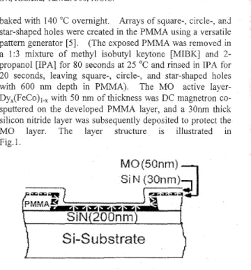
baked with 140 "C overnight Arrays of square-, circle-, and star-shaped holes were created in the PMMA using a versatile pattern generator [SI. (The exposed PMMA was removed in a 1:3 mixture of methyl isobutyl keytone [MIBK] and 2-
propanol [IPA] for 80 seconds at 2.5 OC and rinsed in IPA for 20 seconds, leaving square-, circle-, and star-shaped holes with 600 nm depth in PMMA). The MO active layer- Dy,(FeCo)l., with 50 nm of thickness was DC magnetron co- sputtered on the developed PMMA layer, and a 30nm thick silicon nitride layer was subsequently deposited to protect the MO layer. The layer structure is illustrated in Fig. 1.
S i-S
Ubstrate
Figure 1: The layer structure of a pre-formatted pinning site. The arrows illustrate the MO material magnetization directions.
B. The measurement methods
The sample's morphology and magnetic domain structure were observed by employing an atomic force microscope (AFM) and magnetic force microscope (MFM). A Digital Instruments Nanoscope IIIa SPM, equipped with phase extender [6] was used in this study. The magnetic tip with a CoCr-coated Si tip magnetized along the tip axis was used to scan the magnetic domain structures in the tapping-lift mode [7].
111.
RESULTS AND DISCUSSIONSIn a previous paper[4] we had shown that the magnetic domains had been found to be pinned inside the artificial hole arrays and acquired the geometric shapes of the holes. In this article, we show that nanometer domain structure within circle-, square-, and star-shaped holes could be formed if the pinning hole geometry is not well defined. The measurements we show here is mainly for sample Dy,, 4(Fe80C020)73 6 . , with
I995
perpendicular magnetic anisotropy magnetization 75 emu/cm3 and coercivity of 2.7 kOe.
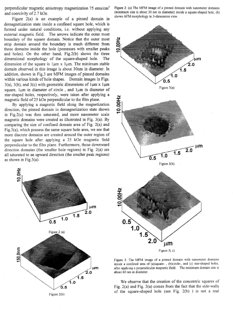
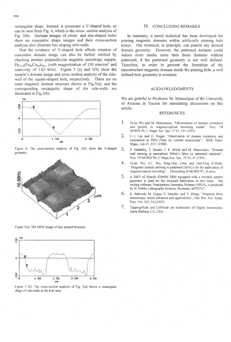
Figure 2(a) is an example of a pinned domain in demagnetization state inside a confined square hole, which is formed under natural conditions, i.e. without applying any external magnetic field. The arrows indicate the outer most boundary of the square domain. Notice that the outer most strip domain around the boundary is much different fiom those domains inside the hole (possesses with smaller peaks and holes). On the other hand, Fig.2(b) shows the three dimensional morphology of the square-shaped hole. The dimension of the square is l p m x lpm. The minimum stable domain observed in this image is about 30nm in diameter. In addition, shown in Fig.3 are MFM images of pinned domains within various kinds of hole shapes. Domain images in Figs. 3(a), 3(b), and 3(c) with geometric dimensions of lpm x
1pm
square, lpm in diameter of circle , and lpm in diameter of star-shaped holes, respectively, were taken after applying a magnetic field of 25 kOe perpendicular to the film plane.
By applying a magnetic field along the magnetization direction, the pinned domain in demagnetization state shown in Fig.2(a) was then saturated, and more nanometer scale magnetic domains were created as illustrated in Fig. 3(a). By comparing the size of confined domain area of Fig. 2(a) and Fig.3(a), which possess the same square hole area, we see that more discrete domains are created around the outer region of the square hole after applying a 25 kOe magnetic field perpendicular to the film plane. Furthermore, those downward direction domains (the smaller hole regions) in Fig. 2(a) are all saturated to an upward direction (the smaller peak regions) as shown in Fig.3(a).
Figure 2 (a)
v-"
Figure 2(b)
Figure 2 (a) The MFM image of a pinned domain with nanometer domains (minimum size is about 30 nm in diameter) inside a square-shaped hole, (b) shows AFM morphology in 3-dimension view
N I 0
8
F Figure 3(a) N::
9
0 F Figure 3(b) Figure 3( c)Figure 3 The MFM image of a pinned domain wlth nanometer domains inside a confined area of (a)square- , (b)circle-, and (c) star-shaped holes, after applying a perpendicular magnetic field The minimum domain size IS
about 60 nm in diameter
We observe that the creation of the concentric squares of Fig. 2(a) and Fig. 3(a) comes from th'e fact that the side-walls of the square-shaped hole (see Fig. 2(b) ) is not a real
I996
rectangular shape. Instead, it possesses a V-shaped hole, as can be seen from Fig. 4, which is the cross- section analysis of Fig. 2(b). Domain images of circle- and star-shaped holes show no concentric shape images and their cross-section analyses also illustrate less sloping side-walls.
That the evidence of V-shaped hole affects creation of concentric domain image can also be firther verified by checking another perpendicular magnetic anisotropy sample, Dyzl 4(FesOCo20)78 6 . (with magnetization of 150 emuicm3 and
coercivity of 1.62 kOe). Figure 5 (a) and 5(b) show the sample’s domain image and cross section analysis of the side- wall of the square-shaped hole, respectively. There are no inner magnetic domain structure shown in Fig.S(a), and the corresponding rectangular shape of the side-walls are illustrated in Fig.S(b).
0 l . 0 0 2 . 0 0
V M
Figure 4 The cross-section analysis of Fig 2(b) show the V-shaped geometry
Figure 5(a): The MFM image of four pinned domains.
0
0 0
4
I O 1.00 2 . 0 0 3.00 4.1 0
IV.
CONCLUDING REMARKSIn summary, a novel technical has been developed for pinning magnetic domains within artificially pinning hole arrays. Our technical, in principle, can pattern any desired domain geometry. However, the patterned domains could induce more media noise then those domains without patterned, if the patterned geometry is not well defined. Therefore, in order to prevent the formation of the nanostructure magnetic domain inside the pinning hole, a well defined hole geometry is essential.
ACKNOWLEDGMENTS
We are grateful to Professor M. Mansuripur of the University of Arizona in Tucson for stimulating discussions on this article. REFERENCES
1.
2.
3.
4.
5 .
6.
7 .
Te-ho Wu and M Mansuripur, “Observations of domain nucleation
and growth in magneto-optical recording media” Proc Of MORIS’92, J Magn SOC Jpn 17 S1, 131 (1993)
C -J Lin and D Rugar, “Observation of domain expansion and contraction in TbFe Films by Lorentz microscope”, IEEE Trans Magn , vol-25,2311 (1988)
S Gadetsky, T Suzuki, J K Erwin and M Mansuripur, “Domain wall pinning in amorphous TbFeCo films on patterned substrate”, Proc OfMORIS’94, J Magn SOC J p n , 19 S1,91 (1995)
Te-ho Wu, J C Wu, Bing-Mau Chen and Han-Ping D Shieh, “Magnetic domain pinning in patterned DyFeCo for the application of
magneto-optical recording”,
A 30kV of Hitachi S2460N SEM equipped with a versatile pattern generator is used for the structure fabrication in this study The writing software, Nanopattern Generator Systems (NPGS), is produced by JC Nabity Lithography Systems, Bozeman, MT59717
K Babcock, M Dugas, S Manalis, and V Eliiigs, “Magnetic force microscopy recent advances and applications”, Mat Res SOC Syinp Proc Vol 355,311(1995)
TappingMode and LiftMode are trademarks of Digital Instruments, Santa Barbara, CA, USA
Proceeding of MORIS’97, in press
Figure 5 (b) The cross-section analysis of Fig 5(a) shows a rectangular shape of side-walls in the hole area