應用於WiMAX系統之電子系統層級設計與分析
72
0
0
全文
(2) 應用於 WiMAX 系統之電子系統層級設計與分析 ESL Design and Analysis in WiMAX Baseband Transmitter 研 究 生:呂聖國. Student:Sheng-Kuo Lu. 指導教授:陳紹基 博士. Advisor:Dr. Sau-Gee Chen Dr. Lan-Da Van. 范倫達 博士. 國 立 交 通 大 學 電機學院 IC 設計產業研發碩士班 碩 士 論 文. A Thesis Submitted to College of Electrical and Computer Engineering National Chiao Tung University in partial Fulfillment of the Requirements for the Degree of Master in Industrial Technology R & D Master Program on IC Design July 2007 Hsinchu, Taiwan, Republic of China. 中華民國 九 十 六 年 七 月.
(3) 應用於 WiMAX 系統之電子系統層級設計與分析. 學生:呂聖國. 指導教授:陳紹基 博士 范倫達 博士 國立交通大學. 電機學院 IC 設計產業研發碩士班. 摘. 要. 在本論文中,以 IEEE 802.16e 之基頻傳送端為例,利用 CoWare Platform Architect 建立 ARM-Based 系統晶片虛擬驗證平台進行電子系統層級設計之實作 與分析。依據既定之演算法所撰寫之程式碼在虛擬平台上進行軟體開發、除錯、 最佳化及軟硬體整合設計,以規格要求推估出系統效能之限制範圍來評估系統效 能並逐步進行軟硬體切割產生以下所列的四種不同的軟硬體組態。一、僅使用軟 體執行,二、自軟體部分切割數個功能並使用個別對應的硬體來進行加速,三、 僅使用硬體並將個別的硬體整合為一,四、使用軟體執行 Modulation 並搭配包含 其餘功能的單一硬體加速器。最後再從模擬過程中取得不同的系統組態下的分析 結果,以此進行討論並提出建議,為實作時選擇系統組態之參考。. I.
(4) ESL Design and Analysis in WiMAX Baseband Transmitter. Student:Sheng-Kuo Lu. Advisor:Dr. Sau-Gee Chen Dr. Lan-Da Van. Industrial Technology R & D Master Program of Electrical and Computer Engineering College National Chiao Tung University. ABSTRACT In this thesis, we use electronic system-level (ESL) design methodology to explore IEEE 802.16e baseband transmitter. We use CoWare Platform Architect to implement an ARM-based SoC (system on a chip) virtual platform and use this platform for analysis with the study case. According to the reference SW (software) code and given algorithms, we port it to the virtual platform for SW development, debugging, optimization, and HW (hardware)/SW co-design. Before software porting, we derive the specification’s requirement as the performance boundary and then evaluate performance via function profiling at four different HW/SW configurations as follows. Case 1: SW only, case 2: individual HWs, case 3: one combined HW only, and case 4: modulation in SW and others in a HW accelerator. At last, we discuss the result from simulation and advance the optimized configuration suggestion before commencing implementations. II.
(5) 誌. 謝. 首先感謝指導教授 陳紹基以及范倫達兩位老師在這兩年多以來的悉心指導 與建議,並提供我各方面的協助,使我可以確立並完成我的論文研究。此外,亦 要感謝國家晶片設計中心的周景揚主任及黃俊銘組長在我的研究過程中所提出的 種種建議,讓我找到方向、抓住目標。在此先對四位師長致上由衷的感激。 其次是感謝黃家齊教授與古孟霖學長無私地提供協助,以及曲健全學長、莊 彥澤學長和學弟致良的幫忙,讓我的研究得以順利地進行下去。也要謝謝 MMLab 與 VIPLab 兩間實驗室的夥伴們,以及 IC 設計產業專班的同學們,感謝你們在我 的研究生生活中所帶來的溫馨與歡笑。 最後要感謝家人和親友們的關心、支持與鼓勵,尤其是親愛的爸爸媽媽,你 們讓我可以無後顧之憂的完成學業。還有在靈界的阿公阿嬤,感謝你們給我的信 心與力量,尤其是阿嬤,很遺憾沒來得及讓您見到這篇論文的完成,謹將其中屬 於我倆祖孫的回憶獻給您。. III.
(6) Contents 中文摘要 ................................................................................................................. Ⅰ ABSTRACT ........................................................................................................... Ⅱ ACKNOWLEDGEMENT .................................................................................... Ⅲ CONTENTS ........................................................................................................... Ⅳ LIST OF TABLES ................................................................................................. Ⅵ LIST OF FIGURES .............................................................................................. Ⅷ. Chapter 1. Introduction ........................................................................................ 1. 1.1 Motivation ..................................................................................................... 2 1.2 Thesis Organization....................................................................................... 3. Chapter 2. Fundemental Concepts ...................................................................... 4. 2.1 SystemC Transaction Level Modeling .......................................................... 4 2.2 CoWare Platform Architect ........................................................................... 6 2.3 IEEE 802.16e Baseband Transmitter ............................................................ 8. Chapter 3. Virtual Platform ................................................................................11. 3.1 Platform Built-up .........................................................................................11 3.1.1 Memory Model .................................................................................. 12 3.1.2 Hardware Model Template ................................................................. 15 3.2 Software Optimization and System Profiling ............................................. 19 3.3 HW/SW Partition Configurations ............................................................... 23 3.3.1 Software Only .................................................................................... 23 IV.
(7) 3.3.2 Individual Hardware Accelarators ..................................................... 25 3.3.3 Combined Hardware .......................................................................... 27. Chapter 4. Result and Analysis .......................................................................... 30. 4.1 Profiling Result ........................................................................................... 30 4.2 Performance Analysis and Discussion ........................................................ 45. Chapter 5. Conclusion and Future Work.......................................................... 58. References .............................................................................................................. 60. Autobiography ....................................................................................................... 61. V.
(8) List of Tables Table 2.1: Execution time boundary in different FFT sizes .............................. 10 Table 4.1: Function profiling result in Case 1..................................................... 32 Table 4.2: Memory accesses of functions in Case 1 (cache disabled) ............... 32 Table 4.3: Memory accesses of functions in Case 1 (4k cache) ......................... 33 Table 4.4: Memory accesses of functions in Case 1 (32k cache) ....................... 33 Table 4.5: Total memory accesses in Case 1 ........................................................ 34 Table 4.6: Bus transaction information in Case 1 .............................................. 35 Table 4.7: Function profiling result in Case 2..................................................... 36 Table 4.8: Memory accesses of functions in Case 2 (cache disabled) ............... 36 Table 4.9: Memory accesses of functions in Case 2 (4k cache) ......................... 37 Table 4.10: Memory accesses of functions in Case 2 (32k cache) ..................... 37 Table 4.11: Total memory and HW models accesses in Case 2 ......................... 38 Table 4.12: Bus transaction information in Case 2 ............................................ 39 Table 4.13: Function profiling result in Case 3................................................... 39 Table 4.14: Memory accesses of function in Case 3 ........................................... 40 Table 4.15: Total memory and HW model accesses in Case 3 ........................... 40 Table 4.16: Bus transaction information in Case 3 ............................................ 41 Table 4.17: Function profiling result in Case 4................................................... 42 VI.
(9) Table 4.18: Memory accesses of functions in Case 4 .......................................... 42 Table 4.19: Total memory and HW model accesses in Case 4 ........................... 43 Table 4.20: Bus transaction information in Case 4 ............................................ 44 Table 4.21: Left over cycles for HW accelerator in Case 3 and Case 4 ............ 56. VII.
(10) List of Figures Figure 1.1: An ESL design methodology ............................................................... 2 Figure 2.1: TLM based ESL design flowchart...................................................... 5 Figure 2.2: The ESL tools classification ................................................................ 6 Figure 2.3: Brief flowchart of referenced SW ...................................................... 9 Figure 2.4: Functional block and iteration flow of TX ........................................ 9 Figure 3.1: Block diagram of referenced platform ............................................ 12 Figure 3.2: Block diagram of memory model ..................................................... 13 Figure 3.3: Part of memory_AHB_TLM.h ......................................................... 13 Figure 3.4: Part of memory_AHB_TLM.cpp ..................................................... 14 Figure 3.5: Block diagram of HW model template ............................................ 15 Figure 3.6: HW accelerator TLM model template (header file) ....................... 16 Figure 3.7: HW accelerator TLM model template (function code part 1) ....... 17 Figure 3.8: HW accelerator TLM model template (function code part 2) ....... 17 Figure 3.9: HW accelerator TLM model template (function code part 3) ....... 18 Figure 3.10: Block diagram of platform with channel model ........................... 20 Figure 3.11: Communicate SW with HW accelerator........................................ 21 Figure 3.12: Data type reinterpretation in TLM model .................................... 21 Figure 3.13: Block diagram of platform in Case 1 ............................................. 23 VIII.
(11) Figure 3.14: Function block and program flow in Case 1 ................................. 24 Figure 3.15: Program validation flow ................................................................. 24 Figure 3.16: Block diagram of platform in Case 2 ............................................. 25 Figure 3.17: Function block and program flow in Case 2 ................................. 26 Figure 3.18: Block diagram of platform in Case 3 & Case 4 ............................ 27 Figure 3.19: Function block and program flow in Case 3 ................................. 28 Figure 3.20: Function block and program flow in Case 4 ................................. 29 Figure 4.1: Cache efficiency for function execution time in Case 1 .................. 45 Figure 4.2: Cache efficiency for total memory accesses in Case 1 .................... 46 Figure 4.3: Cache efficiency for bus transactions in Case 1 .............................. 47 Figure 4.4: Function profiling pie chart for Case 1 ........................................... 48 Figure 4.5: Function profiling pie chart for Case 2 ........................................... 49 Figure 4.6: Instructions and time reduction by HW acceleration .................... 50 Figure 4.7: Memory accesses reduction by HW acceleration ........................... 51 Figure 4.8: Execution time comparison between Case 1 and Case 2................ 52 Figure 4.9: Execution time comparison among Case 2, Case 3, and Case 4 .... 53 Figure 4.10: Cache efficiency for execution time in Case 3 and Case 4 ........... 54 Figure 4.11: Cache efficiency for bus transactions in Case 3 ............................ 55 Figure 4.12: Cache efficiency for bus transactions in Case 4 ............................ 55. IX.
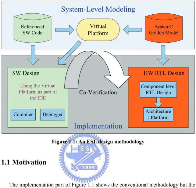
(12) Chapter 1 Introduction. Answering to the increasingly short time-to-market requirement and the growing complexity of electronic devices, and the coming of platform-based design methodologies, SystemC is developed to help address these demands. It had been briefly discussed in the foreword of [1] by Stanley J. Krolikoski, the chairman of the Open SystemC Initiative (OSCI), in March 2002. The shortened time-to-market and growing complexity are also the key challenges in the System on a Chip (SoC) era. Electronic System Level (ESL) design is a front-end process for SoC design, and is a methodology to transform a verified C design to a SoC specification for realization. Figure 1.1 illustrates an ESL design methodology. In the software (SW) design part, it uses a virtual platform as part of the integrated design/development and debug environment (IDE); and in the hardware (HW) register transfer level (RTL) design part, the SystemC golden model used for virtual platform can be reused in the component-level RTL design for functional co-verification. By the same token, the virtual platform which is used for SW early development can be reused to co-verify with real platform after implementation. In the next section, we’ll use this figure to describe our motivation and the goal in this thesis.. 1.
(13) System-Level Modeling Virtual Platform. Referenced SW Code. SystemC Golden Model. . SW Design. HW RTL Design. Using the Virtual Platform as part of the IDE Compiler. Co-Verification. Component level RTL Design. Architecture / Platform. Debugger. Implementation Figure 1.1: An ESL design methodology. 1.1 Motivation The implementation part of Figure 1.1 shows the conventional methodology but the SW development and debug starts with the real platform/architecture; that is, we cannot start SW design before the real platform is ready. The adoption of virtual platform supports early SW development and it can help to overcome the short time-to-market problem. Besides, early exploration of architectures and performance analysis are also the key concern. Gathering enough information and accuracy at high abstraction levels within short time can help getting better architectures before real implementation. For this reason, better model efficiency and reusability than before are important to support higher simulation speed and low complexity. Some beyond 3G wireless broadband networks have been announced. For examples, the mobile WiMAX IEEE 802.16e-2005 technology standard supports advanced 2.
(14) wireless broadband services for computing, portable multimedia, interactive and other consumer electronic devices [2]. For designing WiMAX system [3] in portable devices, we focus on the System-Level Modeling part of ESL design methodology and taking IEEE 802.16e baseband transmitter as our study case to conduct architectural and performance analysis in SW profiling and HW/SW partition configurations on virtual platform in this thesis.. 1.2 Thesis Organization The rest of this thesis is organized as follows. Chapter 2 introduces the fundamental concepts of the virtual platform environment that we use, including the introduction to SystemC Transaction Level Modeling (TLM), CoWare Platform Architect ESL tool, and the study case – IEEE 802.16e Baseband Transmitter. Chapter 3 gives the detail of the built virtual platform and the application software, with all the skills we use, and then describe several simulation configurations in figures. In chapter 4 we’ll discuss the simulation results of our analysis and make suggestion. Finally, the conclusion and the future work are made in chapter 5.. 3.
(15) Chapter 2 Fundamental Concepts. In this chapter, the fundamental concepts will be given, including the introduction to SystemC TLM, CoWare Platform Architect, and the referenced SW code – IEEE 802.16e baseband transmitter.. 2.1 SystemC Transaction Level Modeling Transaction Level Modeling (TLM) is a higher abstraction level than Register Transfer Level (RTL), and uses to reduce the SoC design complexity by higher hardware abstraction level and help system designers to design larger systems. Some classifications of transaction level models are introduced by Lukai Cai and Daniel Gajski [4]. There are several programming languages can be used at transaction level, such as C/C++, System Verilog, and so on; but using SystemC is more convenient for programmers who are familiar with C/C++ because SystemC is based on the C++ programming language. Since the referenced SW code was written in C++ programming language and the CoWare Platform Architect ESL tool supports SystemC IP and SystemC Modeling Library, thus we use SystemC programming language at transaction level. SystemC is both a system level and hardware description language, it can model designs at RTL or at algorithmic level. At the beginning of the design development, the. 4.
(16) needed hardware simulation model at system level should have full functionality, so are as RTL or gate level circuit. It must define the corrected circuit behavior according to the specification, but it doesn’t need to consider how to design the real circuit. For this reason, design a TLM component should be easier than design a RTL component with the same functionalities, and the needed simulation time should be shorter, too. Figure 2.1 is an example of TLM-based ESL design flow, the four major used cases for TLM and the particular ESL design task supported by each of them is introduced by Tim Kogel and Matthew Braun in [5]. In our study case, the Functional View (FV) corresponds to the referenced SW code for IEEE 802.16e baseband TX; the Architect View (AV) corresponds to the platform environment; the Programmers View (PV) corresponds to the application SW development on the platform; and the Verification View (VV) corresponds to the HW and SW implementation, which is not our concern at present time. In other words, the main work in this thesis is among AV and PV used cases.. Figure 2.1: TLM based ESL design flowchart [5] 5.
(17) Using function calls for communication is the defined foundation of TLM by the OSCI TLM working group [6]. It can minimize the number of events and the amount of information that have to be processed during simulation. In a virtual platform, we have three main types of components. They are instruction-set simulator (ISS), bus model, and peripheral models such as memories and HW accelerators. Bus model for platform simulation have different simulation speed/accuracy trade-off in PV, AV, and VV used cases. Because we need some timing information to estimate the performance for architectural exploration, an AV bus model should be suitable for our study case. The ISS and bus model can be directly come from well developed ESL tools, but the application specified peripheral models should be created by ourself. We use SystemC TLM to model them, with Platform Architect Interface (CoWare TLM API) rather than with a wrapper to avoid wrapping delay problem.. 2.2 CoWare Platform Architect [7]. MetaBin. MBin FP (Simulink). Bin. Bin F (Matlab). Bin P (Quartus II). MBin FM (DK). MBin PM (…) Bin M (VTOC) MBin FPM (System Studio). Figure 2.2: The ESL tools classification 6.
(18) Figure 2.2 simply shows the ESL tools classification in [8] with three bins, and the meta-bins consist of two or more bins. F stands for functionality, and P and M represent platform environment and mapping, respectively. Functionality indicates functional representations of a design completely independent of implementation architectures. Platform concerns the modules used to implement the functional description. Mapping refers to instances of the design in which the functionality has been assigned to a set of correctly interconnected modules. With this classification, CoWare ConvergenSC (the predecessor of Platform Architect) is in metabin PM, which means it combines architectural services and mapping. Coware Platform Architect can do SystemC platform capture and reconfiguration by Platform Creator graphical user-interface (GUI) which supplies rapid assembly and reconfiguration of hierarchical SoC Platforms. It also supports architecture analysis for Platform-driven ESL Design. The details can be read in its datasheet [9]. In our study case, we use this ESL tool and it’s supported libraries to build a virtual platform. The Platform Creator GUI supports for drag-and-drop assembly of SystemC transaction level platforms. We can see it as an architecture modeler, which manage to create and modify SystemC Transaction Level Architecture. The design procedure is as follows: place blocks and nodes, complete connections, create the memory map, set parameters for each block, export system, and then we can build and run simulation on the exported system – a virtual platform. The used ISS is ARM926EJS processor support package (PSP), the used bus model is AMBA bus library (BL), and the default TLM level bus simulation model follows AMBA 2.0 specification [10] and helps designs for reusability [11]. We use ARM Symbolic Debugger (ASD) as the simulation user interface, load an ARM executable image into the virtual platform and run system simulation with ISS, bus simulator, and OSCI simulation kernel. The system profiling integrate HW/SW profiling with CoWare 7.
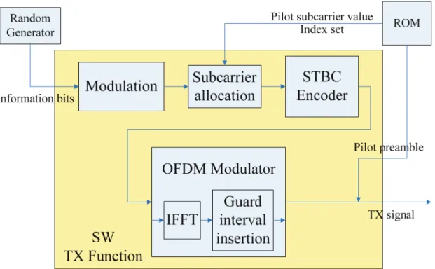
(19) profiling utilities; besides, we simply add some variables in TLM models to easily gather the information we want.. 2.3 IEEE 802.16e Baseband Transmitter Our study case is porting an IEEE 802.16e baseband referenced SW code in C++ programming language to the built virtual platform with several different HW/SW configurations. In this section, we will introduce both of them. WiMAX is the abbreviation of Worldwide Interoperability for Microwave Access, a name for those Wireless Metropolitan Area Network (WMAN) communication devices which follow the IEEE 802.16 wireless communication standard [12]. IEEE 802.16 can be divided into two parts, i.e., fixed WMAN and mobile WMAN. The IEEE 802.16e is the standard for mobile WMAN, based on IEEE 802.16-2004 plus mobility consideration. Because of the mobility, WiMAX 16e system is suitable for portable devices, and can be used in vehicles. Our referenced SW code is composed of three parts, namely, the transmitter (TX), the channel model, and the receiver (RX). It simulate the IEEE 802.16e baseband transmission, by randomly creating information bits throughout the TX part to produce the transmit signals, and then putting the transmit signals on the multi path channel model in different velocities (V) and signal to noise ratios (SNR) to simulate the received signals. After the received signals are demodulated by the RX part, the decided bits will be compared with the information bits to get the average bit error rate (BER). Figure 2.3 shows the briefly flowchart of the referenced SW code. It is useful in algorithmic level, for programmers to verify their algorithms and to evaluate their performances, but that’s not our concern.. 8.
(20) Figure 2.3: Brief flowchart of referenced SW. We are working on architecture exploration to gather architectural and performance analyses for finding suitable system configuration to run the prescribed algorithms on portable devices. Thus the first thing we should do is to trace the referenced SW code, and calculate the execution time boundary according to the specification. Therefore, we cut out the channel model part and the RX part from the referenced SW code, keep only the TX part and modify it to a single iteration for later analysis. The functional block and iteration flow diagram is shown in Figure 2.4.. Figure 2.4: Functional block and iteration flow of TX 9.
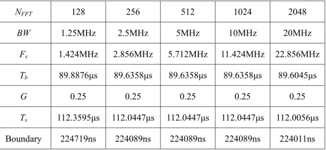
(21) It transmits a frame during the iteration, and the number of Orthogonal Frequency Division Multiplexing (OFDM) symbols in each frame is two. Thus the execution time boundary is equal to two OFDM symbol times. Equation (2.1) represents the OFDM symbol time, where the useful symbol time Tb is from equations (2.2) and (2.3), and the length of Guard Interval (GI) and the OFDM symbol length in the referenced SW code are 64 and 320, respectively. As such, the GI ratio is G =. 1 . Table 2.1 lists the 4. bandwidth (BW) in different Fast Fourier Transform (FFT) sizes, and the corresponding OFDM symbol time. In our performance analysis, we must make sure that the whole TX function can be completed within the time boundary. OFDM symbol time Ts = (1 + G ) Tb Useful symbol time Tb =. (2.1). N FFT Fs. (2.2). 8 7. Sampling frequency Fs = floor ( × BW ×. 1 ) × 8000 8000. (2.3). Table 2.1: Execution time boundary in different FFT sizes NFFT. 128. 256. 512. 1024. 2048. BW. 1.25MHz. 2.5MHz. 5MHz. 10MHz. 20MHz. Fs. 1.424MHz. 2.856MHz. 5.712MHz. 11.424MHz. 22.856MHz. Tb. 89.8876μs. 89.6358μs. 89.6358μs. 89.6358μs. 89.6045μs. G. 0.25. 0.25. 0.25. 0.25. 0.25. Ts. 112.3595μs. 112.0447μs. 112.0447μs. 112.0447μs. 112.0056μs. Boundary. 224719ns. 224089ns. 224089ns. 224089ns. 224011ns. 10.
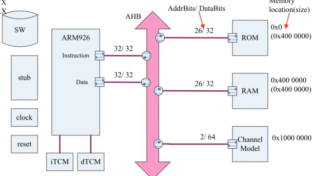
(22) Chapter 3 Virtual Platform. After the introduction in the previous chapters, we can see the virtual platform as a SW model of a HW SoC platform. And we also know what a virtual platform can do, and what its characteristics are. We are trying to confirm them in experimental study case, do HW platform architecture exploration and optimization, do SW development, debugging, optimization, do HW/SW co-design, and additionally to feel the high simulation speed, the flexibility, and the usability for users who are not experts in HW designs. In the following of this chapter, we’ll describe the virtual platform we used in detail and the analysis flow of the study case step by step, and then give several different HW/SW partition configurations. Besides, all the skills that we used to improve the system performance will be also discussed in this chapter.. 3.1 Platform Built-up Figure 3.1 shows the block diagram of our virtual platform in the beginning. We use CoWare Platform Architect and its supported IP libraries (ARM926EJS_AHB_PSP, AMBA BL, Auxiliary, Peripherals) to build it [13]. The design procedure includes place block and nodes, complete connections, create the memory map, set parameters, export system as a virtual platform, and then we can use it to build and run simulations.. 11.
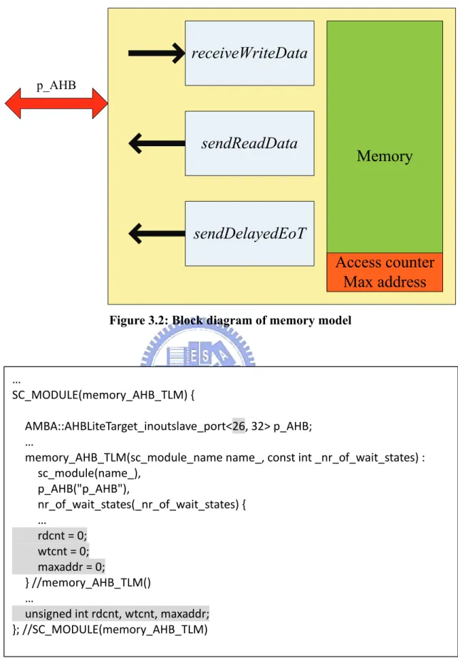
(23) AHB SW. 20/ 32. ARM926 Instruction. stub. Data. Memory location(size). AddrBits/ DataBits. ROM. 0x0 (0x100000). RAM. 0x400 0000 (0x100000). 32/ 32 32/ 32 20/ 32. APB. clock reset. 1/ 8 iTCM. Display. 0xc000 0000 (0x1). dTCM. Figure 3.1: Block diagram of referenced platform For later analysis in HW/SW partition, we put some effort in building our own library [14] (with SystemC TLM models,) and use it to build our virtual platform in different system configurations. The user defined block library includes memory TLM models and HW accelerated TLM models. In the next two subsections we’ll introduce those TLM models in detail.. 3.1.1 Memory Model In order to gather some memory statistics such as read/write access counts and the minimum needed memory space, we modified the SystemC memory TLM model in the Peripheral block library from the CoWare Training Class. Figure 3.2 illustrates the memory model and Figure 3.3 and 3.4 are part of the memory module’s source code, where the reverse texts point out what we modified, which refer to the Access counter & Max address block in Figure 3.2.. 12.
(24) receiveWriteData p_AHB. sendReadData. Memory. sendDelayedEoT Access counter Max address Figure 3.2: Block diagram of memory model. … SC_MODULE(memory_AHB_TLM) { AMBA::AHBLiteTarget_inoutslave_port<26, 32> p_AHB; … memory_AHB_TLM(sc_module_name name_, const int _nr_of_wait_states) : sc_module(name_), p_AHB("p_AHB"), nr_of_wait_states(_nr_of_wait_states) { … rdcnt = 0; wtcnt = 0; maxaddr = 0; } //memory_AHB_TLM() … unsigned int rdcnt, wtcnt, maxaddr; }; //SC_MODULE(memory_AHB_TLM) Figure 3.3: Part of memory_AHB_TLM.h. 13.
(25) … void memory_AHB_TLM::receiveWriteData() { … if ((address + accessSize/8) > maxaddr) maxaddr = address + accessSize/8; wtcnt++; … } //memory_AHB_TLM::receiveWriteData() void memory_AHB_TLM::sendReadData() { … if (address == 0x3fffff8) { p_AHB.ReadDataTrf‐>setReadData(wtcnt); } else if (address == 0x3fffffc) { p_AHB.ReadDataTrf‐>setReadData(rdcnt); } else if (address == 0x3fffff4) { p_AHB.ReadDataTrf‐>setReadData(maxaddr); } else { … if ((address < 0x3ffffe0) && ((address + accessSize/8) > maxaddr)) maxaddr = address + accessSize/8; rdcnt++; } … } //memory_AHB_TLM::sendReadData() Figure 3.4: Part of memory_AHB_TLM.cpp To obtain the statistics we are interested in, first we simply introduce two counters, rdcnt for read access counts and wtcnt for write access counts. The counter rdcnt counts up 1 for every sendReadData() function call, while wtcnt counts up 1 for every receiveWriteData() function call. For the second purpose, we set the address width for port p_AHB to 26 to fill the memory map with 64Mb memory space, then use a register maxaddr to record the maximum address which had been accessed during the simulation process, to evaluate the needed memory space in system. Considering different addressing modes, the maximum address of a memory access would be the sum of the variable address and the variable accessSize/8. The three values can be gotten by reading the last 12 bytes of the memory model. Finally, the variable nr_of_wait_states of this memory TLM model is used in the send end of transaction 14.
(26) function for determines the delay latency of the memory accesses when using CoWare TLM API.. 3.1.2 Model Template In addition to modify memory TLM models, we also created a template for modeling HW accelerators which is illustrated in Figure 3.5. There are two main purposes of our TLM model template. One of the purposes is similar to that in the memory model, which use counters rdcnt and wtcnt to record read and write access counts of a HW accelerator TLM model. Although this information can be received by tracing SW code or recording with SW, however, it’s more convenient and better for analysis without additional useless memory accesses by recording with TLM model. The other purpose is making the sendReadData() function a multi-cycle access function, and adding the system clock to its sensitive list to ensure the data reading from the model is correct and simulate the HW delay issue if needed. Figure 3.6 is the header file of the HW accelerator TLM model template, followed by the function code of the model template in Figure 3.7, Figure 3.8, and Figure 3.9.. receiveWriteData. tri_w. p_AHB. sendReadData. ready. tri_r. Delay Process. Figure 3.5: Block diagram of HW model template 15. other functions.
(27) SC_MODULE(HW_AHB_TLM) { AMBA::AHBLiteTarget_inoutslave_port<1, 32> p_AHB; sc_in<bool> clk_p; sc_in<bool> rst_n; SC_HAS_PROCESS(HW_AHB_TLM); sc_signal<bool> ready, flag, tri_r, tri_w; unsigned int rdcnt, wtcnt, clkcount; void receiveWriteData(); void sendEoT(); void sendReadData(); void checkReady(); void cl_flag(); HW_AHB_TLM(sc_module_name name_) : sc_module(name_), p_AHB("p_AHB"), clk_p("clk_p"), rst_n("rst_n") { SC_METHOD(receiveWriteData); sensitive << p_AHB.getReceiveWriteDataTrfEventFinder(); dont_initialize(); SC_THREAD(sendReadData); sensitive_pos << clk_p; sensitive << ready; dont_initialize(); SC_METHOD(sendEoT); sensitive << p_AHB.getSendEotTrfEventFinder(); dont_initialize(); SC_METHOD(checkReady); sensitive_pos << clk_p; sensitive_neg << rst_n; sensitive << flag; dont_initialize(); SC_METHOD(cl_flag); sensitive << tri_w << tri_r; dont_initialize(); } //HW_AHB_TLM() ~HW_AHB_TLM() { } //~HW_AHB_TLM() }; //SC_MODULE(HW_AHB_TLM) Figure 3.6: HW accelerator TLM model template (header file) 16.
(28) #define DELAY_HW 0 void HW_AHB_TLM::checkReady() { if (!rst_n.read()) { clkcount = 0; ready = 0; } else if (clk_p.read()) { if (flag.read()) { if (clkcount >= DELAY_HW) { ready = 1; clkcount = 0; } else { ready = 0; clkcount++; } } else { ready = 0; clkcount = 0; } } } void HW_AHB_TLM::cl_flag() { if (tri_r.read() != tri_w.read()) flag = 1; else flag = 0; } Figure 3.7: HW accelerator TLM model template (function code part 1) #define Addr_name 0 … void HW_AHB_TLM::receiveWriteData() { p_AHB.getWriteDataTrf(); unsigned int address = p_AHB.WriteDataTrf‐>getAddrTrf()‐>getAddress(); switch (address) { case Addr_name: … if (tri_w.read()) tri_w = 0; else tri_w = 1; break; … default: cout << "Access Error!" << endl; } wtcnt++; if (p_AHB.getEotTrf()) p_AHB.sendEotTrf(); } //HW_AHB_TLM::receiveWriteData() Figure 3.8: HW accelerator TLM model template (function code part 2) 17.
(29) void HW_AHB_TLM::sendReadData() { while (1) { if (p_AHB.getReadDataTrf()) { unsigned int address = p_AHB.ReadDataTrf‐>getAddrTrf()‐>getAddress(); unsigned long long datatemp; switch (address) { case Addr_name: while (!ready.read()) wait(); … if (tri_r.read()) tri_r = 0; else tri_r = 1; p_AHB.ReadDataTrf‐>setReadData(datatemp); break; … default: cout << "Access Error!" << endl; p_AHB.ReadDataTrf‐>setReadData(0); } rdcnt++; p_AHB.sendReadDataTrf(); } if (p_AHB.getEotTrf()) p_AHB.sendEotTrf(); wait(); } //while(1) } //HW_AHB_TLM::sendReadData() void HW_AHB_TLM::sendEoT () { // p_AHB.getEotTrf(); // p_AHB.sendEotTrf(); } //HW_AHB_TLM::sendEoT() Figure 3.9: HW accelerator TLM model template (function code part 3). We add clock clk_p and reset rst_n to the TLM model template as input signals. The cl_flag() function models a combinational logic with an exclusive-or gate to raise the signal flag while the signal tri_w is not equal to the signal tri_r. The value of tri_w will be inverted when the model finish receiving input data and starting its behavior, and tri_r will be inverted when the model finish sending output data and preparing for the next inputs. The checkReady() function models a sequential logic, while the value of signal flag is true, it starts counting up the counter value clkcount, and will raise the. 18.
(30) signal ready when the value of clkcount is larger than or equal to the defined delay cycle of the model; otherwise, the ready signal remains low. The sendReadData() function uses SC_THREAD process to allow multi-cycle accesses, a read transaction cannot get data until the ready signal is raised up. Thus the end of transactions is handled by sendReadData() and receiveWriteData() functions, and the sendEoT() function will do nothing. Finally, the usage of counters rdcnt and wtcnt is the same as in the memory model we described in the previous subsection, and in the meantime we finish creating a template of HW accelerator TLM modes. It means, almost all HW TLM models in our virtual platform are created from this template and using its properties.. 3.2 Software Optimization and System Profiling After building a virtual platform, we still need to build application software for running simulation. In this section, we’ll describe the adopted SW optimization methods step by step during the system profiling and performance analysis. Besides, the HW/SW interface will be introduced in the beginning of using HW accelerators. We want to know where the system bottleneck is, then deal with it. The referenced SW function profiling is the first step, and it can give us the information such as number of function calls and the function execution time. SW profiling results depend on many factors, from SW to HW, compiler to microprocessor and other components. In order to make a comprehensive survey of profiling, we integrate it with system performance analysis. That is, the SW profiling is completed on porting application SW to the used virtual platform, by applying CoWare profiling utilities. According to the profiling result, we can optimize the functions of the application SW in execution time by reducing function calls, instructions of function, and etc. 19.
(31) TX RX. AHB SW. 26/ 32. ARM926 Instruction. stub. Data. Memory location(size). AddrBits/ DataBits. ROM. 0x0 (0x400 0000). RAM. 0x400 0000 (0x400 0000). 32/ 32 32/ 32 26/ 32. clock 2/ 64. reset iTCM. Channel Model. 0x1000 0000. dTCM. Figure 3.10: Block diagram of platform with channel model. Figure 3.10 is the block diagram of our platform after the first step. In this platform, ROM and RAM are modeled by the modified memory TLM model, APB and the Display models are removed, and Channel Model is added on AHB. Display model is not necessary here. We can use the supported semihosting by ARM926 PSP to display values for debugging. Channel Model replaces the corresponding part of referenced SW code because of the large amounts of floating-point arithmetic. During our exploration, we don’t need to consider the precision or the algorithm at this time, but we need to make sure the program result is correct while increasing performance by making any kind of change. Thus the Channel Model uses 64bit data bits and its I/O mapped to AHB address 0x10000000, so that we don’t need to change data type in SW code. Figure 3.11 is an example SW function code of communicating with the Channel Model HW accelerator, and Figure 3.12 represents the data type reinterpretation in the HW accelerator TLM model.. 20.
(32) void Channel(Complex tx_data, Complex rx_data) { #define reg1 (*((volatile double *)0x10000000)) //for Real part #define reg2 (*((volatile double *)0x10000008)) //for Imaginary part // Send tx_data to Channel Model reg1 = tx_data.Real(); reg2 = tx_data.Imaginary(); // Receive rx_data from Channel Model rx_data.Set(reg1, reg2); } Figure 3.11: Communicate SW with HW accelerator. unsigned int access; unsigned long long tempin; double datain, dataout; void HW_AHB_TLM::receiveWriteData() { … access++; if (access < 2) { tempin = p_AHB.WriteDataTrf‐>getWriteData(); } else { access = 0; tempin |= p_AHB.WriteDataTrf‐>getWriteData() << 32; datain = reinterpret_cast<double &>(tempin); } … } //HW_AHB_TLM::receiveWriteData() void HW_AHB_TLM::sendReadData() { unsigned long long datatemp; … datatemp = reinterpret_cast<unsigned long long &>(dataout); access++; if (access == 2) { access = 0; p_AHB.ReadDataTrf‐>setReadData(datatemp >> 32); } else { p_AHB.ReadDataTrf‐>setReadData(datatemp); } … } //HW_AHB_TLM::sendReadData() Figure 3.12: Data type reinterpretation in TLM model 21.
(33) Since the HW TLM model has the same behavior as the original SW functions, we can simply copy them from SW to HW TLM model with a little change on I/O. In this case, the adoption of the Channel Model HW accelerator TLM model decreases the simulation time by about 30k seconds, from over 96% of total execution time to under 0.4%, and reduce 98.4% of ROM accesses and 94.6% of RAM accesses. Although the HW TLM model doesn’t consider timing and is not cycle-accurate, the improvement of simulation speed and the advantages of using it is obvious, and it is also can be used in the simulation of a HW/SW co-design for the users who may even don’t know how to design a HW. But in the second step, we keep only the TX part from the referenced SW code as our application SW, and of course, the Channel Model HW was removed. It is because we want to focus on TX first and avoid other parts to affect the performance analysis. In this step, we avoid semihosting by writing the values of pilot subcarriers value, index set, and pilot preamble from text file to SW code as constant variables. We also use several variables to record the frequently used value as a table for reducing math library function calls. Besides, rewrite SW code by reducing heavy arithmetic with bitwise and/or logical operations and loop unrolling are the other effective optimization techniques. After the second step, in the performance analysis we found almost the execution time in every function is much more than the time constraint. Therefore, we use the same method as channel model in the first step to create several HW accelerator TLM models in the third and later steps. Several HW/SW partition configurations are created for architectural exploration and system performance analysis. One can show the flexibility of the virtual platform by simply and quickly creating a virtual platform with different configurations. Those HW/SW partition configurations are described in detail in the next section. 22.
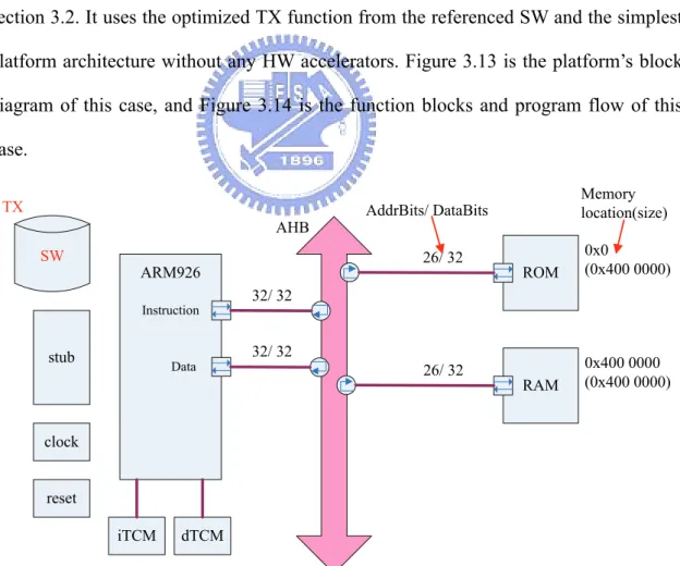
(34) 3.3 HW/SW Partition Configurations In this section, three main classes of HW/SW partition configurations will be described in different subsections separately: no HW, individual HWs, and one combined HW. Each subsection may have more than one simulation cases, and we’ll illustrate the platform and the program flow with each simulation case for clear and easy explanation.. 3.3.1 Software Only The simulation case of this subsection is the one introduced in the second step of section 3.2. It uses the optimized TX function from the referenced SW and the simplest platform architecture without any HW accelerators. Figure 3.13 is the platform’s block diagram of this case, and Figure 3.14 is the function blocks and program flow of this case. TX AHB SW. 26/ 32. ARM926 Instruction. stub. Data. Memory location(size). AddrBits/ DataBits. ROM. 0x0 (0x400 0000). RAM. 0x400 0000 (0x400 0000). 32/ 32 32/ 32 26/ 32. clock reset iTCM. dTCM. Figure 3.13: Block diagram of platform in Case 1. 23.
(35) Figure 3.14: Function block and program flow in Case 1 Since there is no HW accelerators used in this simulation case, we take this case as the referenced case and use is as the program validation for the other configurations. Figure 3.15 shows the program validation flow, where the SW golden function TX1 comes from this case, and the partitioned function TX2 come from the other configurations.. Random number generator. TX1 (SW golden function). TX signal_1. Comparator Information bits. TX2 (Partitioned function). TX signal_2. Figure 3.15: Program validation flow 24. Match ?.
(36) Before system profiling with any simulation case, we run this validation flow to make sure that the modification is functionally correct for those changes which are modified in whether SW C++ program or HW SystemC TLM models. After validation passes, we can be assured that the modification for a new configuration is correct, therefore we can remove the SW golden functions and run simulation again with analyses such as bus information and function profiling.. 3.3.2 Individual Hardware Accelerators The individual HW accelerators subsection explains platform architectures which include one or more individual HW accelerators. After step 3 in section 3.2, we add a HW accelerator which is corresponding to the new bottleneck function to improve system performance step by step. Figure 3.16 and Figure 3.17 illustrate the block diagram of the platform and program flow with function blocks in simulation Case 2 which represents the configuration after step 5. TX AHB SW. 26/ 32. ARM926 Instruction. stub. Data. ROM. 0x0 (0x400 0000). RAM. 0x400 0000 (0x400 0000). 32/ 32 32/ 32. 26/ 32. 1/ 64 clock 2/ 64 reset. 2/ 64 iTCM. Memory location(size). AddrBits/ DataBits. dTCM. Modulator 0x800 0800 STBC 0x800 0400 Encoder FFT 0x800 0000 IFFT. Figure 3.16: Block diagram of platform in Case 2. 25.
(37) Random Generator. HW. Information bits. Modulation. Pilot subcarrier value Index set. Subcarrier allocation. HW STBC Encoder. Pilot preamble. OFDM Modulator Guard interval insertion. IFFT SW Part. TX signal. HW Figure 3.17: Function block and program flow in Case 2. We keep only this simulation case for the next chapter in this subsection against the third type of configuration in the next subsection. Actually, this floating-point version application SW consumes double numbers of the bus transactions in HW acceleration because of the use of the 64-bit IEEE 754 double precision floating-point data type. We have three methods to solve this problem. The first method is adapting the application SW to a fixed-point version. However, this is not suitable for our aim to do early exploration. The second method is simulating with 64-bit bus, and we need to modify the memory models and the used ISS should support 64 bits, too. The third method is what we used for our study case. We adjust the HW/SW configuration to ignore or clear the influences of 64-bit float-point data. In other words, we simplified the bus transactions between HW/SW interfaces by using only one combined HW accelerator. Therefore, we can easily make a conversion of transaction counts from 64-bit to 32-bit if needed. Further discussion of this will give in the next section. 26.
(38) 3.3.3 Combined Hardware In this subsection, the using of combined HW means we only have one HW accelerator TLM model on our platform of the configuration type. Thus we only have one block diagram of virtual platform with this configuration, which is shown in Figure 3.18. The combined HW accelerator includes several HW function blocks and their interconnections, so we can reduce the bus transactions between each HW function block and the SW. Although it may increase the area cost and complexity of the corresponding HW, it can simplify the problem from the viewpoint of platform architecture. Using different SW program structures and their corresponding HW accelerators may create many different new configurations, so that we can have many different configurations in the type classified in this subsection. Any fine tune may lead to a different configuration and analysis result with some different assumptions. We’ll discuss two concluded configurations in this subsection, named the simulation Case 3 and Case 4.. Figure 3.18: Block diagram of platform in Case 3 & Case 4. 27.
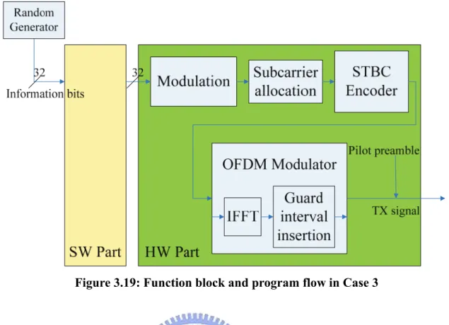
(39) Figure 3.19: Function block and program flow in Case 3. Figure 3.19 illustrates the program flow of simulation Case 3. Obviously, we don’t see any function block inside the SW part in this case. That is, we simulate a configuration that all function blocks in the baseband TX are run within the HW. In this case, the SW part mainly handles the parameter setting for each HW function block. Besides, it will be used in validation. But still, we can see an assumption here. We assume the input information bits are in 32-bit data format and they are sent to HW accelerator directly. We may need a data buffer if the input information bits are not 32-bit data, or decrease the transaction data width to increase bus transaction counts, which can be regarded as other configurations based on this simulation case. Another concluded configuration is illustrated in Figure 3.20, which is our simulation Case 4. In this case, the Modulation function block is moved from the HW part to the SW part. This configuration should be more suitable for representing HW/SW co-design on our virtual platform.. 28.
(40) Random Generator 32 Information bits. U n p a c k. 2. M o d u l a t i o n. 64. Subcarrier allocation. STBC Encoder. OFDM Modulator IFFT. SW Part. Guard interval insertion. Pilot preamble. TX signal. HW Part. Figure 3.20: Function block and program flow in Case 4. In this simulation case, we use the same assumption on the input information bits as in Case 3. In order to support the three different modulation modes, i.e., QPSK, 16QAM, and 64QAM, we need an unpacking process to handle the input information bits. In this simulation case, Figure 3.18 shows the 16QAM modulation, and the real part value and the imaginary part value are modulated in turns, so that the unpacking process unpacks input data to 2 bits. Besides, we can see the modulated output in this case is in 64-bit double precision floating-point data format. By the same token, we could create many different configurations based on this case to discuss it. One method is encoded the modulated output to 4-bit no matter what modulation mode has been used, and then we can send the 4-bit encoded data to the HW part or buffered the encoded data to utilize the 32bit bus width. Or we could use fixed-point data format which is lower than 32bit to represent the modulated output without additional codec.. 29.
(41) Chapter 4 Result and Analysis. In this chapter, we list the profiling result of the simulation in each simulation case that we defined in the previous chapter, and then use them to do performance analysis. In section 4.1, we’ll list the profiling result in each case and roughly explain how to gather them. In section 4.2, our performance analysis will be shown by comparing with two or more configurations, followed by some discussion.. 4.1 Profiling Result For each simulation case, we first modify the application SW C++ program to make an ARM executable image file with CoWare ARM926T Bootcode and scatter load. Second, we modify HW SystemC TLM models (if needed) to create a virtual platform using Platform Creator. Finally, we build and run simulation with ARM Symbolic Debugger (ASD), load an executable image file, enable analysis function from CoWare profiling utilities, and then wait for result [15]. In addition to the analysis reported by CoWare profiling utilities, we also gather some information by ourselves which had been introduced in chapter 3. But the information is displayed on ASD directly and will affect the performance analysis from CoWare profiling utilities. Thus we make two kinds of executable images for each simulation case, one is adding our profiling code in the functions to print out the. 30.
(42) simulation information without analysis function; the other is without adding the code but just the analysis function from CoWare profiling utilities. Our simulation flow for each case is listed below: first, combined SW golden functions with our modified functions to make sure the modification is functionally correct; second, remove SW golden functions and add our own profiling code to run again; third, remove our own profiling code and run simulation with the enabled analysis function form CoWare profiling utilities. We simulate three supported modulation modes separately for each simulation case and combine the results together. The profiling results include function execution time, memory accesses, bus transactions, etc…. Cache size is one kind of factors that we are interested in. We can adjust both instruction and data cache sizes on the ARM926 PSP by Parameter Editor in Platform Creator. The unit of the size is in kilobytes. Since setting cache size to zero is illegal, we must make another executable image file to disable cache module for the case of without cache. For each simulation case, we have three different results with different cache sizes, which are zero cache, 4k bytes for both instruction and data cache, and 32k bytes for both instruction and data cache. Table 4.1 is the function profiling result for simulation Case 1. We list five main functions in the column of function name, where the indent actions at the beginning of each function name shows the relationship between those functions. The function TX contains the other four functions, and the function OFDM Modulator contains the function IFFT. In other words, the three functions Modulation, STBC Encoder, and OFDM Modulator are called within the function TX, and the function IFFT is called within the function OFDM Modulator. The column of Total execution time in nanosecond is separated into three columns corresponding to three different cache sizes, and the total instruction count for each function is listed, too. 31.
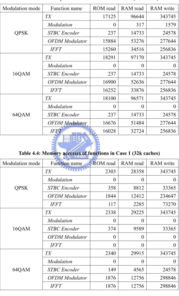
(43) Table 4.1: Function profiling result in Case 1 Modulation mode. Function name TX. Total execution time (Cache size) 0k. OFDM Modulator IFFT TX. 60016. 58552. 5376. 3474940. 1084860. 985424. 59417. 79216600 40976100 40527900. 3099137. 74916100 39559600 39269800. 3013449. 91459200 44870500 44198600. 3364008. Modulation. 272984. 85808. 82688. 8484. 3474940. 1084860. 987000. 59417. 79580700 41054300 40606800. 3129506. 75280300 39637100 39348700. 3043818. 91501400 44996400 44293800. 3376156. STBC Encoder OFDM Modulator IFFT TX Modulation. 64QAM. 318400. 110976. 106120. 6912. 3474940. 1084730. 988480. 59417. 79502700 41103800 40626300. 3140154. 75202300 39687300 39368100. 3054466. STBC Encoder OFDM Modulator IFFT. 3328995. 242736. STBC Encoder. 16QAM. 32k. 91013600 44740300 44067700. Modulation QPSK. 4k. Instruction counts. Table 4.2: Memory accesses of functions in Case 1 (cache disabled) Modulation mode. Function name TX Modulation. QPSK. STBC Encoder OFDM Modulator IFFT TX Modulation. 16QAM. STBC Encoder OFDM Modulator IFFT TX Modulation. 64QAM. STBC Encoder OFDM Modulator IFFT 32. ROM read. RAM read. RAM write. 5926775. 382603. 343745. 28056. 3456. 1920. 164303. 18948. 24579. 5347218. 332080. 277648. 5176510. 315892. 256836. 5928111. 383371. 343745. 30514. 4224. 1920. 164303. 18948. 24579. 5346928. 332080. 277648. 5176220. 315892. 256836. 5949586. 384139. 343745. 43256. 4992. 1920. 164303. 18948. 24579. 5352628. 332080. 277648. 5181920. 315892. 256836.
(44) Table 4.3: Memory accesses of functions in Case 1 (4k caches) Modulation mode. Function name TX Modulation. QPSK. STBC Encoder OFDM Modulator IFFT TX Modulation. 16QAM. STBC Encoder OFDM Modulator IFFT TX Modulation. 64QAM. STBC Encoder OFDM Modulator IFFT. ROM read. RAM read. RAM write. 17125. 96644. 343745. 0. 317. 1579. 237. 14733. 24578. 15884. 53276. 277644. 15260. 34516. 256836. 18291. 97170. 343745. 0. 0. 0. 237. 14733. 24578. 16900. 52636. 277644. 16252. 33876. 256836. 18100. 96571. 343745. 0. 0. 0. 237. 14733. 24578. 16676. 51484. 277644. 16028. 32724. 256836. Table 4.4: Memory accesses of functions in Case 1 (32k caches) Modulation mode. Function name TX Modulation. QPSK. STBC Encoder OFDM Modulator IFFT TX Modulation. 16QAM. STBC Encoder OFDM Modulator IFFT TX Modulation. 64QAM. STBC Encoder OFDM Modulator IFFT. 33. ROM read. RAM read. RAM write. 2303. 28358. 343745. 0. 0. 0. 358. 8812. 33365. 1844. 12412. 234647. 117. 2285. 73270. 2338. 29225. 343745. 0. 0. 0. 374. 9589. 33365. 0. 0. 0. 0. 0. 0. 2340. 29915. 343745. 0. 0. 0. 149. 4565. 24578. 1876. 12756. 298846. 1876. 12756. 298846.
(45) Table 4.2 is the memory access count for each function with disabled caches in simulation Case 1, and Table 4.3 and Table 4.4 show the same information in the same simulation case but running with 4k and 32k for both instruction and data caches. These tables are similar to Table 4.1 but the listed values are changed to ROM read access counts, RAM read access counts, and RAM write access counts. These access counts were gathered by additional profiling variables which accumulate the difference in total memory access counts from the counters in the memory model between the begin position and the end position during each function call. Table 4.5 shows total memory read/write access counts in simulation Case 1 with different cache sizes. This information is gathered by running the other executable images without additional profiling variables and code in previous three tables. Table 4.5: Total memory accesses in Case 1 Modulation mode. QPSK. 16QAM. 64QAM. Read 6607357 6897407 7179063 ROM access counts Write. 0. 0. 0. Total 6607357 6897407 7179063. Cache disabled. Read. 405351. 419175. 432999. RAM access counts Write. 389362. 401678. 413994. Total. 794713. 820853. 846993. Read. 43094. 43747. 43332. ROM access counts Write. 0. 0. 0. Total. 43094. 43747. 43332. Read. 91814. 93966. 95254. RAM access counts Write. 389075. 401391. 413707. Total. 480889. 495357. 508961. Read. 26598. 26715. 26676. ROM access counts Write. 0. 0. 0. Total. 26598. 26715. 26676. Read. 28670. 29422. 30174. RAM access counts Write. 389075. 401391. 413707. Total. 417745. 430813. 443881. I-cache: 4k D-cache: 4k. I-cache: 32k D-cache: 32k. 34.
(46) Table 4.6 is the bus transaction information in simulation Case 1 gathered by CoWare profiling utilities. Table 4.6: Bus transaction information in Case 1 Modulation mode. Information Type Transaction Counts Transaction Throughputs (kB/s). QPSK. Bus Utilization (%) Master Wait Total (%). Master. Transaction Throughputs (kB/s) 16QAM. Bus Utilization (%) Master Wait Total (%). Transaction Throughputs (kB/s) 64QAM. Bus Utilization (%) Master Wait Total (%). 4k. 32k. 6609320. 36936. 24912. DAHB. 912442. 489451. 421683. IAHB. 258975. 2958.45. 2024.27. DAHB. 35658.1. 39191.8. 34252.8. IAHB. 53.038. 0.605891. 0.41457. DAHB. 7.3221. 8.028886. 7.01739. IAHB. 1.58846. 0.0116303. 0.00737214. DAHB. 15.626. 3.11136. 3.08761. 0.172145. 0.0312299. 0.0309498. IAHB. 6891390. 38109. 25053. DAHB. 946646. 503391. 434735. IAHB. 258158. 2900.02. 1932.16. DAHB. 35350.5. 38296. 33516.7. IAHB. 52.8708. 0.593925. 0.395706. DAHB. 7.26267. 7.84529. 6.86653. IAHB. 1.5213. 0.0115796. 0.0069181. DAHB. 15.4394. 3.03037. 3.01443. 0.169607. 0.0304195. 0.0302134. IAHB. 7165550. 37606. 24982. DAHB. 980599. 517299. 447843. IAHB. 258087. 2723.58. 1834.01. DAHB. 35190.8. 37454.4. 32866.9. IAHB. 52.8562. 0.55779. 0.375605. DAHB. 7.23332. 7.67282. 6.73333. IAHB. 1.51992. 0.00998225. 0.00661541. DAHB. 15.3297. 2.9779. 2.95016. 0.168497. 0.0298788. 0.0295677. AVG. Waiting Masters Transaction Counts. 0k. IAHB. AVG. Waiting Masters Transaction Counts. Cache size. AVG. Waiting Masters. The following tables show the simulation results for other simulation cases.. 35.
(47) Table 4.7: Function profiling result in Case 2 Modulation mode. Function name. Total execution time (Cache size) 0k. 4k. 32k. 15316600. 5629390. 5351670. 305841. 202832. 166072. 166072. 3840. STBC Encoder. 1126790. 592280. 582760. 20490. OFDM Modulator. 5908480. 2239900. 2066220. 116444. 1608190. 828416. 808200. 30760. 15365800. 5655700. 5377680. 307377. 202832. 166024. 166024. 3840. STBC Encoder. 1126790. 592328. 582792. 20490. OFDM Modulator. 5908480. 2240100. 2066730. 116444. 1608190. 828224. 808208. 30760. 15425800. 5682720. 5406250. 310449. 202832. 166024. 166024. 3840. STBC Encoder. 1126790. 592328. 582688. 20490. OFDM Modulator. 5908480. 2240090. 2067290. 116444. 1608190. 828224. 808232. 30760. TX Modulation QPSK. IFFT TX Modulation 16QAM. IFFT TX Modulation 64QAM. Instruction counts. IFFT. Table 4.8: Memory accesses of functions in Case 2 (cache disabled) Modulation mode. Function name. ROM read. RAM read. RAM write. 739811. 54439. 72565. Modulation. 21889. 1920. 1920. STBC Encoder. 60930. 3075. 5123. 271008. 21324. 25928. 100364. 5132. 5132. 743392. 55207. 72565. Modulation. 23041. 2688. 1920. STBC Encoder. 60930. 3075. 5123. 271008. 21324. 25928. 100364. 5132. 5132. 747559. 55975. 72565. Modulation. 28033. 3456. 1920. STBC Encoder. 60930. 3075. 5123. 271008. 21324. 25928. 100364. 5132. 5132. TX QPSK. OFDM Modulator IFFT TX 16QAM. OFDM Modulator IFFT TX 64QAM. OFDM Modulator IFFT 36.
(48) Table 4.9: Memory accesses of functions in Case 2 (4k caches) Modulation mode. Function name. ROM read. RAM read. RAM write. 1086. 52524. 72565. Modulation. 87. 685. 3883. STBC Encoder. 77. 2029. 5122. 324. 21916. 25924. 148. 3412. 5128. 966. 53316. 72565. Modulation. 87. 701. 1939. STBC Encoder. 77. 2029. 5122. 260. 21916. 25924. 84. 3380. 5128. 992. 54118. 72565. 121. 2279. 4363. 77. 2029. 5122. 260. 21916. 25924. 84. 3380. 5128. TX QPSK. OFDM Modulator IFFT TX 16QAM. OFDM Modulator IFFT TX Modulation 64QAM. STBC Encoder OFDM Modulator IFFT. Table 4.10: Memory accesses of functions in Case 2 (32k caches) Modulation mode. Function name. ROM read. RAM read. RAM write. 662. 24908. 72565. Modulation. 0. 0. 0. STBC Encoder. 0. 0. 0. OFDM Modulator. 0. 0. 0. 0. 0. 0. 651. 25713. 72565. Modulation. 0. 0. 0. STBC Encoder. 0. 0. 0. 545. 14831. 46525. 0. 0. 0. 662. 26436. 72565. Modulation. 0. 0. 0. STBC Encoder. 0. 0. 0. OFDM Modulator. 0. 0. 0. 0. 0. 0. TX QPSK. IFFT TX 16QAM. OFDM Modulator IFFT TX 64QAM. IFFT. 37.
(49) Table 4.11: Total memory and HW models accesses in Case 2 Modulation mode. QPSK. 16QAM. 64QAM. Read 1416541 1691722 1968445 ROM access counts Write. 0. 0. 0. Total 1416541 1691722 1968445. Cache disabled. Read. 77182. 91006. 104830. RAM access counts Write. 118175. 130491. 142817. Total. 195357. 221497. 247647. Read. 26416. 26185. 26571. ROM access counts Write. 0. 0. 0. Total. 26416. 26185. 26571. Read. 52918. 53686. 54462. RAM access counts Write. 117898. 130214. 142530. Total. 170816. 183900. 196992. Read. 24912. 24665. 25059. ROM access counts Write. 0. 0. 0. Total. 24912. 24665. 25059. Read. 25342. 26110. 26894. RAM access counts Write. 117898. 130214. 142530. Total. 143240. 156324. 169424. Read. 1536. 1536. 1536. Write. 768. 768. 768. Total. 2304. 2304. 2304. Read. 4096. 4096. 4096. Write. 1024. 1024. 1024. Total. 5120. 5120. 5120. Read. 4096. 4096. 4096. Write. 2052. 2052. 2052. Total. 6148. 6148. 6148. I-cache: 4k D-cache: 4k. I-cache: 32k D-cache: 32k. Modulation HW access counts. STBC Encoder HW access counts. IFFT HW access counts. There is a little difference between Table 4.11 and Table 4.5, because Case 2 of Table 4.11 uses three individual HW accelerators whose access counts are also listed.. 38.
(50) Table 4.12: Bus transaction information in Case 2 Modulation mode. Information Type Transaction Counts Transaction Throughputs (kB/s). QPSK. Bus Utilization (%) Master Wait Total (%). Master. Transaction Throughputs (kB/s) 16QAM. Bus Utilization (%) Master Wait Total (%). Transaction Throughputs (kB/s) 64QAM. Bus Utilization (%) Master Wait Total (%). 4k. 32k. 1498210. 23802. 23562. DAHB. 250097. 192404. 163484. IAHB. 243941. 9638.86. 9852.26. DAHB. 40584.1. 77857.7. 68299.3. IAHB. 49.9592. 1.97404. 2.01774. DAHB. 8.33972. 15.9572. 14. IAHB. 1.3294. 0.0352477. 0.0329697. DAHB. 17.447. 5.73128. 5.86466. 0.187764. 0.0576653. 0.0589763. IAHB. 1765700. 23691. 23315. DAHB. 283917. 205496. 176568. IAHB. 244796. 7643.2. 7710.54. DAHB. 39165.5. 66250.7. 58345.5. IAHB. 50.1342. 1.56533. 1.57912. DAHB. 8.06135. 13.5777. 11.9589. IAHB. 1.19672. 0.028213. 0.0271596. DAHB. 16.6372. 4.93952. 5.0181. 0.178339. 0.0496774. 0.0504526. IAHB. 2034920. 24077. 23677. DAHB. 317763. 218604. 189700. IAHB. 245490. 6440.26. 6467.13. DAHB. 38093.6. 58435. 51775.3. IAHB. 50.2763. 1.31897. 1.32447. DAHB. 7.85089. 11.9754. 10.6116. IAHB. 1.10768. 0.0232272. 0.0221519. DAHB. 16.0548. 4.39389. 4.44984. 0.171625. 0.0441711. 0.0447199. AVG. Waiting Masters Transaction Counts. 0k. IAHB. AVG. Waiting Masters Transaction Counts. Cache size. AVG. Waiting Masters. Table 4.13: Function profiling result in Case 3 Modulation Function Total execution time (Cache size) Instruction mode name counts 0k 4k 32k QPSK. TX. 5176. 3992. 3992. 123. 16QAM. TX. 10168. 8144. 7856. 243. 64QAM. TX. 15160. 12008. 11720. 363. 39.
(51) Table 4.14: Memory accesses of functions in Case 3 Modulation mode Cache size Function name. QPSK. 16QAM. 64QAM. ROM. RAM. read. read write. 0k. TX. 213. 26. 3. 4k. TX. 0. 0. 0. 32k. TX. 0. 0. 0. 0k. TX. 405. 50. 3. 4k. TX. 0. 0. 0. 32k. TX. 0. 0. 0. 0k. TX. 597. 74. 3. 4k. TX. 0. 0. 0. 32k. TX. 0. 0. 0. Table 4.15: Total memory and HW model accesses in Case 3 Modulation mode. QPSK Read 283810. 559794. 839382. 0. 0. 0. Total 283810. 559794. 839382. ROM access counts Write Cache disabled. 16QAM 64QAM. Read. 15133. 28981. 42829. RAM access counts Write. 13829. 26169. 38509. Total. 28962. 55150. 81338. Read. 4798. 4911. 5124. ROM access counts Write. 0. 0. 0. Total. 4798. 4911. 5124. Read. 1000. 2064. 1800. RAM access counts Write. 13552. 25892. 38232. Total. 14552. 27956. 40032. Read. 4790. 4911. 5124. ROM access counts Write. 0. 0. 0. Total. 4790. 4911. 5124. Read. 992. 1352. 1736. RAM access counts Write. 13552. 25892. 38232. Total. 14544. 27244. 39968. Read. 0. 0. 0. Write. 24. 48. 72. Total. 24. 48. 72. I-cache: 4k D-cache: 4k. I-cache: 32k D-cache: 32k. TX HW access counts. 40.
(52) Table 4.16: Bus transaction information in Case 3 Modulation mode. Information Type Transaction Counts Transaction Throughputs (kB/s). QPSK. Bus Utilization (%) Master Wait Total (%). Master. Transaction Throughputs (kB/s) 16QAM. Bus Utilization (%) Master Wait Total (%). Transaction Throughputs (kB/s) 64QAM. Bus Utilization (%) Master Wait Total (%). 4k. 32k. 300599. 5771. 5731. DAHB. 38973. 15789. 15755. IAHB. 248057. 8296.62. 8244.11. DAHB. 31485.1. 22524.2. 22491.1. IAHB. 50.8023. 1.69915. 1.68839. DAHB. 6.58656. 4.64873. 4.64154. IAHB. 0.491968. 0.0209044. 0.0203279. DAHB. 13.0944. 2.50588. 2.50387. 0.135683. 0.0252679. 0.0252419. IAHB. 568312. 5908. 5828. DAHB. 72865. 29201. 28481. IAHB. 249642. 4547.9. 4493.76. DAHB. 31394.6. 22385. 21867. IAHB. 51.1267. 0.93141. 0.920323. DAHB. 6.5551. 4.60361. 4.49755. IAHB. 0.559385. 0.0110357. 0.0108961. DAHB. 12.6499. 2.2445. 2.23385. 0.132093. 0.0225553. 0.0224475. IAHB. 840627. 6105. 6033. DAHB. 106757. 41333. 41253. IAHB. 249641. 3109.74. 3073.59. DAHB. 31118.3. 20992.1. 20954.9. IAHB. 51.1265. 0.636874. 0.62947. DAHB. 6.4929. 4.31186. 4.30425. IAHB. 0.539773. 0.00865847. 0.00834703. DAHB. 12.6321. 2.05208. 2.05107. 0.131719. 0.0206074. 0.0205942. AVG. Waiting Masters Transaction Counts. 0k. IAHB. AVG. Waiting Masters Transaction Counts. Cache size. AVG. Waiting Masters. We combined all TX function blocks to one HW accelerator for simulation Case 3, so that only TX function remains in the application SW program.. 41.
(53) Table 4.17: Function profiling result in Case 4 Modulation mode QPSK 16QAM 64QAM. Total execution time (Cache size) Instruction counts 0k 4k 32k. Function name TX Modulation TX Modulation TX Modulation. 392512. 175496. 175400. 8501. 242152. 71400. 71360. 5376. 379472. 176224. 176120. 8889. 226616. 70928. 70888. 5716. 477608. 217360. 216808. 10157. 323712. 112368. 111952. 6912. Table 4.18: Memory accesses of functions in Case 4 Modulation mode Cache size Function name 0k QPSK. 4k 32k 0k. 16QAM. 4k 32k 0k. 64QAM. 4k 32k. TX Modulation TX Modulation TX Modulation TX Modulation TX Modulation TX Modulation TX Modulation TX Modulation TX Modulation. ROM read. RAM read. write. 24560 1568. 7. 24507 1562. 3. 0. 0. 0. 0. 0. 0. 0. 0. 0. 0. 0. 0. 22318 1592. 7. 22265 1586. 3. 0. 0. 0. 0. 0. 0. 0. 0. 0. 0. 0. 0. 34677 1616. 7. 34623 1610. 3. 0. 0. 0. 0. 0. 0. 0. 0. 0. 0. 0. 0. Table 4.17 and Table 4.18 have one more function than Table 4.13 and Table 4.14, because simulation Case 4 retains the function Modulation from application SW code.. 42.
(54) Table 4.19: Total memory and HW model accesses in Case 4 Modulation mode. QPSK Read 314888. 589902. 885465. 0. 0. 0. Total 314888. 589902. 885465. ROM access counts Write Cache disabled. 16QAM 64QAM. Read. 16956. 30804. 44653. RAM access counts Write. 14212. 26552. 38893. Total. 31168. 57356. 83546. Read. 14737. 14818. 15167. ROM access counts Write. 0. 0. 0. Total. 14737. 14818. 15167. Read. 1332. 2356. 2156. RAM access counts Write. 13945. 26285. 38626. Total. 15277. 28641. 40782. Read. 14737. 14818. 15159. ROM access counts Write. 0. 0. 0. Total. 14737. 14818. 15159. Read. 1316. 1700. 2124. RAM access counts Write. 13945. 26285. 38626. Total. 15261. 27985. 40750. Read. 0. 0. 0. Write. 1536. 1536. 1536. Total. 1536. 1536. 1536. I-cache: 4k D-cache: 4k. I-cache: 32k D-cache: 32k. TX HW access counts. The twenty tables in this section show the profiling result of simulations for the four simulation cases that we had defined in chapter 3, and three supported modulation modes run with three different configurations in cache size of ISS for each case. All of the results in these tables are simulated in a 125MHz system clock frequency; that means the system clock period is 8 ns. All TLM models for HW accelerators are seen as ideal HW without delay although we had defined delay parameter and ready signal in model template, and the bus transaction duration is also 8 ns.. 43.
(55) Table 4.20: Bus transaction information in Case 4 Modulation mode. Information Type Transaction Counts Transaction Throughputs (kB/s). QPSK. Bus Utilization (%) Master Wait Total (%). Master. Transaction Throughputs (kB/s) 16QAM. Bus Utilization (%) Master Wait Total (%). Transaction Throughputs (kB/s) 64QAM. Bus Utilization (%) Master Wait Total (%). 4k. 32k. 330283. 15784. 15536. DAHB. 43585. 18152. 18136. IAHB. 246996. 20644.5. 20331.4. DAHB. 31969.4. 23559.2. 23551.3. IAHB. 50.585. 4.22799. 4.16386. DAHB. 6.6753. 4.86229. 4.8607. IAHB. 0.609714. 0.0195542. 0.0179569. DAHB. 13.6969. 2.84366. 2.84363. 0.143066. 0.0286321. 0.0286158. IAHB. 597722. 15729. 15656. DAHB. 77453. 31532. 30860. IAHB. 247778. 11467.2. 11430.9. DAHB. 31522.1. 22886.6. 22429.9. IAHB. 50.7451. 2.34848. 2.3412. DAHB. 6.57555. 4.70801. 4.61451. IAHB. 0.600564. 0.0116461. 0.0113643. DAHB. 13.1682. 2.40387. 2.39458. 0.137687. 0.0241552. 0.0240595. IAHB. 885043. 15990. 15926. DAHB. 111323. 43697. 43633. IAHB. 250197. 7815.68. 7786.46. DAHB. 30908.6. 21290.3. 21264.6. IAHB. 51.2404. 1.60065. 1.59467. DAHB. 6.44514. 4.37421. 4.36896. IAHB. 0.551284. 0.00830857. 0.00821064. DAHB. 12.9417. 2.17805. 2.17792. 0.13493. 0.0218636. 0.0218613. AVG. Waiting Masters Transaction Counts. 0k. IAHB. AVG. Waiting Masters Transaction Counts. Cache size. AVG. Waiting Masters. 44.
數據
+7

相關文件
The starting point for Distance (Travel Distance) for multi-execution of the motion instruction is the command current position when Active (Controlling) changes to TRUE after the
On the other hand Chandra and Taniguchi (2001) constructed the optimal estimating function esti- mator (G estimator) for ARCH model based on Godambes optimal estimating function
(In Section 7.5 we will be able to use Newton's Law of Cooling to find an equation for T as a function of time.) By measuring the slope of the tangent, estimate the rate of change
In particular, we present a linear-time algorithm for the k-tuple total domination problem for graphs in which each block is a clique, a cycle or a complete bipartite graph,
• To introduce the use of the LPF as a tool for planning the school English Language curriculum; and
Understanding and inferring information, ideas, feelings and opinions in a range of texts with some degree of complexity, using and integrating a small range of reading
利用 determinant 我 們可以判斷一個 square matrix 是否為 invertible, 也可幫助我們找到一個 invertible matrix 的 inverse, 甚至將聯立方成組的解寫下.
Then, we tested the influence of θ for the rate of convergence of Algorithm 4.1, by using this algorithm with α = 15 and four different θ to solve a test ex- ample generated as
Numerical results are reported for some convex second-order cone programs (SOCPs) by solving the unconstrained minimization reformulation of the KKT optimality conditions,
