國 立 交 通 大 學
光電工程學系碩士班
碩士論文
次世代基板成長高效率氮化鎵系列發光二極體之研究
Research of High performance Nitride based Blue Light Emitting
Diode Growth on Next Generation Templates
研 究 生 :劉哲宇
指導教授 :紀國鐘 教授
i
次世代基板成長高效率氮化鎵系列發光二極體之研究
Research of High performance Nitride based Blue Light Emitting Diode Growth on Next Generation Templates 研究生:劉哲宇 Student:Che-Yu Liu 指導教授:紀國鐘 教授 Advisor:Gou-Chung Chi 國 立 交 通 大 學 光 電 工 程 學 系 碩 士 班 碩 士 論 文 A Thesis
Submitted to Institute of Electro-Optical Engineering College of Electrical Engineering
National Chiao Tung University in Partial Fulfillment of the Requirements
for the Degree of Master
In
Electro-Optical Engineering July 2012
Tainan, Taiwan, Republic of China
ii
次世代基板成長高效率氮化鎵系列發光二極體之研究
研究生 : 劉哲宇 指導教授 : 紀國鐘教授 國立交通大學光電工程學系碩士班
摘要
在本研究中,我們利用 metal-organic chemical vapor deposition (MOCVD) 將氮化 鎵系列之發光二極體成功的成長在火山口狀圖形化藍寶石基板以及內嵌中空空氣孔洞 及二氧化矽之氮化鎵奈米柱基板。
在火山口狀圖形化藍寶石基板上成長的發光二極體 (CPSS-LEDs) 研究中,從穿 隧電子顯微鏡 (Transmission electron microscopy, TEM) 拍攝的圖片中我們可以明顯的 指出缺陷(dislocation)有著彎曲倒像在圖形化基板側壁的趨勢。 而從上視的陰極光偵 測系統所擷取之圖可以發現 CPSS-LEDs 有著較均勻的發光圖形。除此之外,從掃描 式電子顯微鏡所 (Scanning electron microscopy, SEM)拍之截面圖可以發現在圖形化基 板之上有著甜甜圈形狀的空氣孔洞。此空氣孔洞有藉由光散射效應進而增加光萃取效 率之可能性,這是由於空氣本身和氮化鎵磊晶層有著極大的折射率差異,導致光從氮 化鎵欲進入空氣時有著極小的全反射角,進而使的光能夠反射而使萃取效率提升。 再 來我們對光強度、電流對電壓作圖來研究其電學特性可以發現成長在半球型圖形化基 板 (Hemisphere patterned sapphire substrate, HPSS) 和成長在火山狀圖形化基板 (CPSS) 之發光二極體相對於成長於一般藍寶石基板之發光二極體 (C-LEDs)在二十毫安培操
iii 作電流下,光強度有著百分之二十以及百分之三十二之提升。名為 Tracepro 的光學 模擬軟體在我們想要進一步了解光萃取效率提升的目標下被使用。從光學模擬的結果 中,在主動區設定 10 毫瓦強度之發光源之下,成長於三種基板上之發光二極體分別在 遠場之積分球上收到 3.57 毫瓦、5.41 毫瓦以及 5.69 毫瓦之光強度。此結果也和我們的 實驗結果趨勢吻合。 在我們成功成長發光二極體結構於 CPSS 上的基礎上,我們開始考慮將發光二極 體成長於奈米等級的結構之上。為了將發光二極體的效率提高已達到更好的應用目的, 我們想藉由奈米等級的結構進一步的降低缺陷密度以及提高光萃取效率來達成我們的 目的。最後,我們選擇了氮化鎵奈米柱的基板來達到我們的需求。 在發光二極體成長於氮化鎵奈米柱基板的研究中,我們可以從掃描式電子顯微鏡 (SEM) 中明顯的觀察到微米級的空氣孔洞和奈米級的二氧化矽在奈米柱之間和在奈 米柱及再成長之氮化鎵磊晶層之間。空氣孔洞及二氧化矽和氮化鎵磊晶層的折射率差 可以有效的提高光萃取效率。而從穿隧式電子顯微鏡 (TEM) 所截取的圖中可以發現, 藉由 nanoscale epitaxial lateral overgrowth (NELOG) 效應使得線缺陷彎曲而隱沒在空 氣孔洞以及二氧化矽中。進一步地,我們利用室低溫的變強度光學量測 (PDPL) 來定 義內部量子效率來驗證磊晶品質的提升。 最後,藉著 Finite-difference time domain
(FDTD) 模擬來進一步的驗證光萃取的效率。從光學量測和光學模擬的結果中,我們 得知內部量子效率和光萃取效率分別有了 15 % 和 44 %的提升。
iv
Research of High Performance Nitride based Blue Light Emitting Diode
Growth on Next Generation Templates
Student: Che-yu Liu Advisor: Dr. Gou-Chung Chi
Institute of Electro-Optical Engineering
National Chiao Tung University
Abstract
In this research, the high performance GaN-based light-emitting diodes
(LEDs) growth on crown-shaped pattern sapphire substrates (CPSS) and GaN
nanorods template with embedded microscale air voids and SiO
2nanomask by
metal–organic chemical vapor deposition (MOCVD) were demonstrated.
From transmission electron microscopy (TEM) image, we can clearly
observed the dislocation bending. And the plan-view cathodoluminescence
(CL) image shows the light uniformity of CPSS-LEDs. Besides, by
cross-sectional scanning electron microscopy (SEM), donut-shaped air voids
on the top of the crown PSS have been observed. These air voids is consider to
enhance the light scattering effect and further enhance the light extraction due
to the huge difference reflective index between air voids and GaN epilayer.
From the power-current-voltage (L-I-V) characteristic, we can figure out the
light output power enhancement of hemisphere patterned sapphire substrate
v
is about 20 % and 32.1 % under 20 mA, respectively. For the purpose to prove
light extraction enhancement, the Tracepro simulation have been used.
According to the simulation result, we find out the output power of three
sample are 3.57 mW, 5.41 mW and 5.69 mW where we give the total emission
power is 10 mW. This result is well agree with our L-I measurement.
Based on the research of CPSS-LEDs, we start to considering the nano
structure inside the epitaxial layer. For the wish to push the efficiency of
nitride-based LEDs reach the application needed, we expect the nano structure
can reduce more dislocation and enhanced higher light extraction due to
density of patterned. Finally, the GaN nanorods template have been
demonstrate to satisfy our purpose.
Microscale air voids and SiO
2nanomask were clearly observed at the
interface between GaN nanorods (NRs) and the overgrown GaN layer by
scanning electron microscopy (SEM). The difference reflective index between
air voids (SiO
2) and GaN can increase the light extraction efficiency due to
additional total reflection. The transmission electron microscopy (TEM)
images show the threading dislocations were suppressed by nanoscale epitaxial
lateral overgrowth (NELOG). To quantify the internal quantum efficiency
vi
temperature and low temperature has been used. And the finite-difference time
domain (FDTD) simulation was also be used to calculate the light extraction
efficiency. From the PL measurement and FDTD simulation, we estimate the
vii
致謝
兩年的碩士班生涯轉瞬即逝,腦中卻有萬千的回憶,似乎在花下另一個兩年也回 憶不完。這本碩士論文所包含的不只有著新時代的知識也包含著滿滿的回憶以及滿滿 的感謝。在這裡,我要感謝老師、學長姐、學弟妹以及同學們的幫助來讓我度過碩士 班的生涯。 感謝紀國鐘老師在生活中的關心以及對於人生方向及目標上的提點,讓我能夠在 遇到問題的時候不只著墨於如何解決問題達成成果,而是將實驗上的挫敗視為成功的 契機。 感謝郭浩中老師在領導團隊上面的用心,在老師組織實驗室各組分工的妥善安排 下讓實驗進行得更加順利,而實驗室所舉辦的聚餐及出遊更是讓實驗室的感情更加融 洽,讓我們在研究外也學習到和人相處的方式。 感謝鏡學、Joseph、David、小見、李博、藍博等學長姐在研究上的指導和規劃, 讓我在實驗時總能迅速的達到目標。也讓我在碩士班的兩年之中,總是能有研究的題 材和實驗可以分析。除此之外,在日常生活中讓我們在剛升上碩士班時能迅速的了解 實驗室運作以及在平常時和我們一起吃飯、打球的日子也成為了我碩士班的難忘回憶 之一。 感謝老漢、13、BUSH、康雨婷、萬海、郭炫廷、MO WANG、施懷翔這些碩二同學在 我碩士班生涯的兩年期間,陪伴著我和我一起在實驗室度過實驗煩悶的夜晚,也讓我 在打球、快炒店、好樂迪等等地方留下快樂的回憶。感謝學弟妹,在實驗上的幫助讓 我能夠順利的完成論文中的實驗以進行分析,有了你們讓我的碩士班過得更加的愉 快。 最後,我要感謝我的父母,總是能讓我無後顧之憂的讀書而不用為了生活而苦惱, 而「家」也總是在我實驗遇到挫折時成為避風的港灣。 有了這麼多人的幫助,我才有幸能在碩士班的期間完成這本論文,縱使言語已經 無法表達心中的感謝,我還是要向大家說一聲: 謝謝大家!!viii
CONTENTS
摘要 ... ii Abstract ... iv 致謝 ... vii CONTENTS ... viii List of Figures ... xList of Tables ... xiii
Chapter 1 Introduction ... 1
1.1 Characteristics of Nitride-based Light-emitting diode ... 1
1.2 Development of Nitride-based Light-emitting diode ... 3
1.3 Motivation ... 5
Chapter 2 Properties of Light Emitting Diodes ... 8
2.1 Internal Quantum Efficiency (IQE) ... 8
2.2 External Quantum Efficiency (EQE) and Light Extraction Efficiency (LEE) ... 12
Chapter 3 Experiment Instrument and Simulation Tools ... 14
3.1Metal-organic Chemical Vapor deposition system ... 14
3.2 Photoluminescence system ... 16
3.3 TracePro Light Tracing Simulation ... 19
3.4 Finite-Difference Time Domain (FDTD) Simulation ... 20
Chapter 4 Crown-shaped Patterned Sapphire Substrate (CPSS) ... 21
4.1 Fabrication of PSS and LED Devices ... 21
4.2 Crystal Quality of GaN Epitaxial Layer ... 25
4.3 Optical Characteristic of CPSS LEDs ... 27
4.4 Electrical Characteristic of CPSS-LEDs ... 30
4.5 TracePro Simulation Results of Crown-shaped PSS LED ... 32
ix
5.1 Fabrication of Gallium Nitride Nanorods Template ... 37
5.2 Crystal Quality of Bulk GaN Epitaxial Layer ... 44
5.3 Observation of Dislocation in GaN epitaxial layer ... 47
5.5 Electronic Characteristic of Nanorods LED devices ... 56
5.6 Light Extraction Enhancement simulate by FDTD simulation ... 59
Chapter 6 Conclusions ... 63
x
List of Figures
Figure 1.1.1 Band gap at room temperature ... 2
Figure 3.1.1 MOCVD Growth Mechanisms ... 15
Figure 3.2.1 The setup detail of Ti:sapphire laser PL system. ... 18
Figure 3.2.2 The setup detail of He-Cd laser PL system. ... 18
Figure 4.1.1 The fabrication flow of CPSS ... 23
Fig 4.1.2 SEM images for (a) tilted image of CPSS, (b) cross section of HPSS,(c) cross-sectional of CPSS-LEDs. (b) The magnified view of air avoids on top of the crown shape. ... 24
Figure 4.1.3 LED structure growth on CPSS and the LED device with n-contact and p-contact. ... 24
Figure 4.2.2 Efficiency versus dislocation density of different material... 26
Figure 4.3.1 Power-dependent PL measurement at 15 K and 300 K of CPSS-LEDs, HPSS-LEDs and C-LEDs ... 29
xi
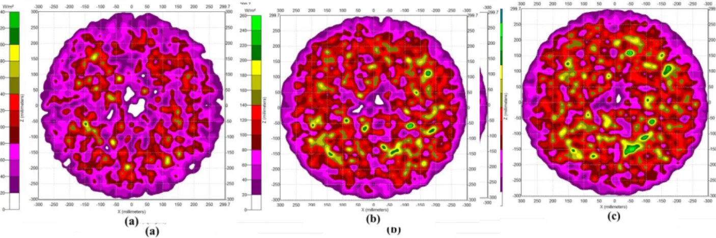
Figure 4.5.1 Tracepro simulation of candela map taken from InGaN LEDs grown on (a)
C-LEDs, (b) HPSS-LEDs and (c) CPSS-LEDs ... 34
Figure 4.5.2 Optical properties as function of crater angle for the crown-shaped ... 35
patterned. The insert shows crater of CPSS. ... 35
Figure 5.1.1 Fabrication flow of GaN nanorods ... 39
Figure 5.1.2 (a) Cross-section and (b) tilted SEM of GaN nanorods. ... 40
Figure 5.1.3 Sketch of NELOG process ... 41
Figure 5.1.4 Cross-sectional SEM of re-growth u-GaN epitaxial layer ... 41
Fig 5.1.5 AFM image of (a) u-GaN on nanorods, (b) u-GaN on sapphire ... 42
Figure 5.1.6 LED structure growth on nanorods template and the LED device with n-contact and p-contact... 43
Figure 5.2.1 Raman spectrum of E2 high peak ... 46
xii
Figure 5.3.1 Cross-sectional TEM images of GaN epilayer overgrown on GaN NRs
template (a) under two-beam condition for g D 1N100, (b) under two-beam condition for g
D 0002, (c) HRTEM image of region I in (a) and (d) HRTEM image of region II in (b). ... 49
Figure 5.4.1 Power-dependent PL measurement at 15 K and 300 K of NR-LEDs ... 54
and C-LEDs. ... 54
Figure 5.4.2 Normalized PL intensity as a function of 1000/T for (a)NR-LED and (b) C-LED. ... 55
Figure 5.5.1 Optical microscopy image of NR-LED and C-LED operated at 20 mA ... 57
Figure 5.5.2 (a) Forward I-V curves of NR-LEDs and C-LEDs ... 58
(b) Reverse I-V curves of NR-LEDs and C-LEDs ... 58
Figure 5.6.1 Simulation parameter of air voids LED and reference LED ... 61
Figure 5.6.2 Light output intensity versus real time ... 61
xiii
List of Tables
Table 4.5.1 Light extraction Tracepro results of C-LED, HPSS-LED and CPSS-LED... 34
1
Chapter 1 Introduction
In this chapter, I will introduce the characteristics and development of nitride-based light emitting diode. Besides, the motivation of this research will also be explained.
1.1 Characteristics of Nitride-based Light-emitting diode
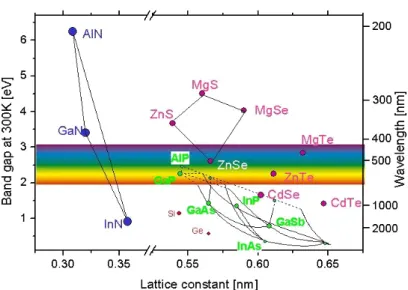
Nowadays, the nitride-based light emitting diodes (LEDs) have been widely used in optoelectronic and electronic devices, because it has wide direct band gap and it cover whole visible light region, from ultraviolet (UV) to infrared (IR) as shown in figure 1.1.
This unique characteristic let nitride-based LEDs have a lot of applications, such as, signboard, traffic signal, back lighting of LCD, automotive lighting, indoor and outdoor lighting [1-4]. Although nitride-based LED has a lot of advantages, it still has several issues need to conquer, and push the LED achieve goal of solid state lighting. For the purpose to achieve this goal, improve the performance of blue LED will be necessary, because the general white light for solid state lighting is produced by blue LED pumping yellow phosphors. If the efficiency of blue LED can be improved, we can increase the lumen per watt (lm/W) of white light LED.
With some unique properties, the III-nitride semiconductor material is not only suitable for lighting source in short wavelength in visible region but also high-speed/high-power electron device [5]. For instance, it has high bond energy (~2.3 eV), high-saturation velocity
2
(~2.7 x 104 cm/s), high-breakdown field (~2 x 10⁶V/cm), and strong excitonic effects (>50 meV) [6-7].
In general, the GaN-based LED efficiency can be expressed as the product of internal quantum efficiency (IQE) and external quantum efficiency (EQE). Due to the large lattice mismatch between substrate and GaN epitaxial layer, it can induce the piezoelectric field and spontaneous electric field which will tilt the band diagram, this effect in the hetero-interface called quantum confined Stark effect (QCSE) and causing charge separation between electrons and holes in quantum wells [8-9]. This effect will decrease the IQE of LED. Besides, the reflective index between GaN epitaxial layer and air are 3.54 and 1, according to the Snell’s law, the total reflective angle will let the light trap inside the GaN
epitaxial layer. Even though it have such disadvantage, it still been believe to have the good potential in solid state lighting.
3
1.2 Development of Nitride-based Light-emitting diode
The first III-nitride materials blue light-emitting diode (LED) was reported by J. I. Pankove et al. at 1972, fabricated it with metal-i-n structure [10]. This huge discover start the research of nitride-based LED, and it has been believe to become the next generation light source. Nevertheless, there were some disadvantage which might pull down the efficiency, and the most important issue is about the substrate for GaN epitaxy. For instance, sapphire substrate with 15% smaller lattice constant compared with GaN, and the different thermal expansion coefficient, which leads to high dislocation density and the crack of epitaxial layer. Therefore, to find a suitable substrate for GaN epitaxial layer will be very important. The problem was firstly solved by Amano and Akasaki by designing and growing a AlN buffer layer in 1986 [11]. Also, Nakamura grew AlGaN buffer layers on top of sapphire in 1991 [12] which make it possible to grow GaN on sapphire. In addition to the invention of buffer layer, Prof. S. Nakamura also solved the high growth temperature problems by his two-flow growth reactor which was beneficial to high quality GaN material on sapphire [13].
Besides, the difficulty of p-type doping is another issue, as we know, every semiconductor lighting device needs p-n junctions. Nevertheless, due to the highly
background n-type concentration which was resulting from the native defects (commonly thought to be nitrogen vacancies) and residual impurities (such as Si and oxygen) acted as an efficient donor, p-type GaN performed poor conductivity. The poor conductivity issue has
4
been improved by Akasaki's work. Akasaki (1988 at Nagoya University) discovered that samples showed p-type conductivity after Low Electron Beam Irradiation treatment (LEBBI)[14-15]. This achievement courage people and showed the possible for p-type doping. Nakamura was then found out the solution to the puzzle of p-type doping. He found that previous investigators had annealed the samples in Ammonia (NH3) atmosphere at high
temperatures. Ammonia dissociates above 400 ℃ , producing atomic hydrogen. Atomic hydrogen then passivates acceptors, so that p-type characteristics are not observed. As a result, Nakamura solved this problem by annealing the samples with nitrogen gas, instead of Ammonia [16].
With the efforts made by predecessors, the blue GaN-based light-emitting diode (LED) is now sucessfully commercialized. Nowadays, a typical blue GaN LED is mainly consisit of substrate, n-type GaN, multiple quantum wells (MQWs), and p-type GaN. The n-type GaN was doped by sillicon (Si) and become as the electorns provider. On the other hand, the p-type GaN was doped by magnesium (Mg) and treat as holes provider, which layer that the electrons have been removed. If a forward bias is applied, electrons and holes can recombine, transfer the energy in the transition layer to the form of light. The energy of the photon corresponds to the voltage bias in the transition region (the “bandgap”). Sapphire and silicon carbide are often used as substrates, which allow for large-area heteroepitaxial growth.
5
1.3 Motivation
Nowadays, the blue GaN-based LED had been development to have such potential for application on solid state lighting. However, it still have a long way to go to reach the application on solid state lighting. There are some drawbacks which limit the efficiency of LED, such as, the huge different reflective index between GaN (n=2.45) and air (n=1) which let the photon emitting from active region trapped inside the GaN epitaxial layers and limit the light extraction efficiency. Although many groups has announced various methods to improved the light extraction by patterned sapphire substrate (PSS) [17-19], it still have much more to do with, such as, the shaped of PSS. On the other hand, internal piezoelectric field and spontaneous polarization at heterointerface leading to the quantum confined Stark effect (QCSE) and causing charge separation between electrons and holes in quantum wells, still deteriorate the lighting efficiency. Besides, the lack of a suitable, inexpensive substrate restrains the improvement of GaN-based devices. Even though many semiconductor companies produce and sell pure GaN substrates today, their prices are always sky-high and not very accessible to ordinary applications.
As we knows, the patterned sapphire substrate have already been used in many companies when they growth the GaN-based LED. However, we believe by tuning the shaped of sapphire's pattern, we can further increase the light extraction of light emitting diode and let more photons emitting to the free space due to the better light scattering effect.
6
In this study, we demonstrate a crown-shaped patterned sapphire substrate formed by dry etching process and optimized the light extraction of the angle of crown. Electro-optical properties of LEDs fabricated by the completed expitaxial structures grown on such GaN NPs template will also be discussed.
In general, GaN-based epitaxial layers were grown on sapphire substrate by heteroepitaxial technique, such as metal-organic chemical vapor deposition (MOCVD) [20, 21]. However, due to the large lattice mismatch and thermal expansion coefficient misfit between GaN and sapphire, the subsequent-grown GaN epitaxial layers contained high threading dislocation densities (TD densities) (around 108-1010 cm-2) [22]. To overcome these high TD densities issue and improved the crystal quality of GaN epitaxial layers on sapphire substrate, various growth techniques have been proposed, such as epitaxial lateral overgrowth (ELOG) [23, 24], cantilever epitaxy (CE) [25], defect selective passivation [26], microscale SiNx or SiOx patterned mask [27-29], anisotropically etched GaN-sapphire interface [30],
plastic relaxation through buried AlGaN cracks [31].
Even with these techniques, it is still difficult to reduce TD density to a level ~10-7 cm-2 unless certain complicated or expensive method such as double ELOG [32] or epitaxy on GaN substrate [33] is used. Recently, nanoscale epitaxial lateral overgrowth (NELOG) was found to be a promising method. During the NELOG process, the crystal quality will be improved and increase the internal quantum efficiency (IQE).
7
In this study, we report a NELOG of high quality GaN layers on high height depth ratios GaN nanorods template fabricated by ion inductive coupled plasma- reactive ion etching (ICP-RIE). In summary, we demonstrate the blue GaN based LED growth on GaN nanorods template, which can improved the crystal quality and enhanced the light extractive efficiency at the same time.
8
Chapter 2 Properties of Light Emitting Diodes
In this chapter, we will introduce several properties which were the key factor when we talk about InGaN based light emitting diode. The physical meaning of internal quantum efficiency (IQE), light extraction efficiency (LEE) and external quantum efficiency (EQE) will be explained.
2.1 Internal Quantum Efficiency (IQE)
The active region of ideal LED emits one photon when one electron injected. Each charge quantum-particle (electron) produces one light quantum-particle (photon). Thus the ideal active region of an LED has a quantum efficiency of unity. The internal quantum efficiency is defined as: (2-1) where Pint is the optical power emitted from the active region and I is the injection
current. h is the plank's constant, ν is the photon frequency relate to the wavelength of active region and e equal to 1.6×10⁻¹⁹ coulomb, which is the electron energy. For an ideal light-emitting diode, all photon emitted from active region will emitted into free space. We will say such LED has unity extraction efficiency. However, in a real light-emitting diode, not every photons emitted from active layer can extract to free space, some of them will be trap in the
9
light-emitting diode. Here is some possible reasons, such as, photons may be reabsorbed by material itself during transport, or light may be incident on metallic contact surface and absorb by metal, and also the photons may trap by the reflection effect appeared at the interface between LED and free space due to the huge difference of reflective index. In addition, the phenomenon of the total internal reflection, also referred to as the trapped light phenomenon, reduces the ability of light to escape from the active region.
There is another view point, the internal quantum efficiency in a semiconductor is related to non-radiative recombination centers. If the radiative lifetime is denoted as τr and the
non-radiative lifetime is denoted as τnr, then the total probability of recombination is given by
the sum of the radiative and non-radiative probability:
(2-2) The relative probability of radiative recombination is given by the radiative probability over the total probability of recombination. Thus the probability of radiative recombination or IQE is given by:
τ τ τ (2-3)
10
According to the equation, we realized that the IQE is given as the ratio of number of light quanta emitted inside the semiconductor to the number of charge quanta undergoing recombination. In other words, we define the IQE as the ratio of the excitation quanta which transfer the energy to radiative recombination and the sum of the excitation quanta which transfer the energy to radiative recombination and non-radiative recimbination. Note that not all photons emitted internally may escape from the semiconductor due to critical angle and reabsorption mechanisms.
By the above equation, the internal quantum efficiency is determined by the competition between radiative and nonradiative recombination processes. In this material system, the radiative recombination rate is affected by the quantum-confined Stark effect (QCSE) and exciton localization effects. Although the relative importance of these contributions has been widely studied in recent years, many questions regarding the emission process still remain.
In general, we used temperature dependent PL measurement and investigate the PL intensity variation curves with temperature to define IQE. It is a non-destructive method to understand the internal material characteristics and quality. It provides useful information about emission wavelength, light intensity and other optical properties. During the experiment period, the intensity reduce with the temperature rise. We could reasonably assume there are no non-radiative recombination at 0 K and the IQE approaches 1 which means one photon generated in the MQW while one laser photon was injected into the MQWs. In the meantime,
11
we assume the extraction would not change with the increasing temperature. Therefore, the IQE could be defined as equation (2-4) by the traditional method:
(2-4) where I(0) and I(T) are attribute to the PL intensity at 0K and specific temperature, respectively. We note that this method ignores the influence of injected laser power density which is not valid in blue GaN-based LED material system. Hence, we quote reference [34] to give a new definition by PL method. We performed the power-dependent PL measurement at low temperature and room temperature and define it by observing the tendency of the curves. This could be expressed as the following equation (2-5):
(2-5) where IPL is the collected PL intensity; Iinj is the injected laser intensity; EPL is the measured
light photon energy; Einj is injected photon energy and C is a constant which is related to carrier
injection efficiency, light extraction efficiency and correction efficiency of PL.
Although PL intensity will increase when we pull up the injected laser power, the ratio between PL intensity divide by injected power will have the maximum number. We can
12
calculate the ratio of collected photons to be divided by injected laser photons, by equation 3-2. Then we observed and normalized the curve by the maximum at low temperature, so we could define the IQE at room temperature with different laser power.
2.2 External Quantum Efficiency (EQE) and Light Extraction Efficiency (LEE)
The extraction efficiency can be a severe limitation for high performance LEDs. It is quite difficult to increase the extraction efficiency beyond 50% without resorting to high sophisticated and costly device processes. The light extraction efficiency (LEE) is defined as:
(2-6) where P is the optical power emitted into free space. Considering the refractive indices of GaN (n ≈ 2.5) and air (n ≈ 1), for the light escape cone is about 23% due to the critical angle. Assuming that light emitted from sidewalls and backside is neglected, one expects that approximately only 4% of the internal light can be extracted from surface. The light outside the escape cone is reflected into the substrate and is repeatedly reflected, then reabsorbed by active layers or electrodes, unless it escapes through the sidewalls. However, there is much room for improvement of the light extraction efficiency. For example, roughening of the top LED surface increased the light extraction efficiency.
13
Finally, the external quantum efficiency (EQE) can defined as:
ν (2-7) from the equation above, we realized that the EQE depend on IQE and LEE, therefore, improve the IQE and LEE will be an important part to reach high performance LED. from the equation above, we realized that the EQE depend on IQE and LEE, therefore, improve the IQE and LEE will be an important part to reach high performance LED. Recently, the patterned sapphire substrate is introduced to improve the IQE which is attributed to reduce the dislocation density and enhance the LEE due light emit to substrate may reflect and emit into free space. In this research, we fabricate light-emitting diode on two different template and analysis the enhancement of IQE and LEE for both semiconductor devices.
14
Chapter 3 Experiment Instrument and Simulation Tools
In this chapter, I will introduce the experiment equipment we have used in our research, and also I will make a description of experimental setup. In addition, the simulation software we have used in this research will also be introduced.
3.1Metal-organic Chemical Vapor deposition system
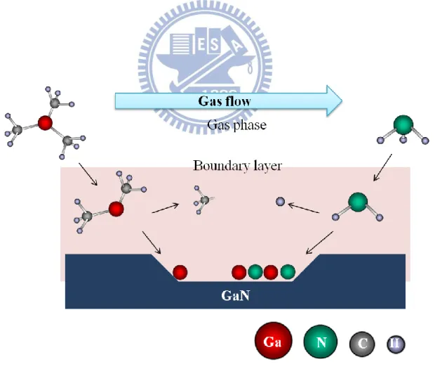
Nowadays, it is well known to growth nitride-based LED by metal-organic chemical vapor deposition (MOCVD) system. In the following research, we growth our LED sample by a low pressure MOCVD (Veeco D75) system.
In general, MOCVD is a method to grow/deposit thin solid films, usually semiconductors, on solid substrates (wafers) using organometallic compounds as sources. The reasons we use MOCVD system to grow nitride-based LED is because of compared with liquid phase epitaxy (LPE), MOCVD system is more stable and the quality is more uniform. Besides, compared with molecular beam epitaxy (MBE), MOCVD system has the higher growth rate and no ultra high vacuum needed. Therefore, the MOCVD system is the most usual way to fabricate the nitride-based semiconductor structure. During the growth, we usually choice trimethylgallium (TMGa), trimethylindium (TMIn) and ammonia (NH3)
were used as gallium, indium, and nitrogen sources, respectively. Silane (SiH4) and
15
The main growth mechanism based on the following chemical formula:
The GaN epitaxial layer was formed by the formula above, during the growth, we can separate the chamber into two region by boundary layer. For the region above boundary layer is the region that the gas flow pass and remain in gas phase, and for the region below the boundary layer, the gas sources transport to the substrate surface by diffusion, and the heat will let the gas sources reaction follow by the formula and deposit the GaN layer. The growth mechanisms sketch was showed as figure 3.1.1.
16
3.2 Photoluminescence system
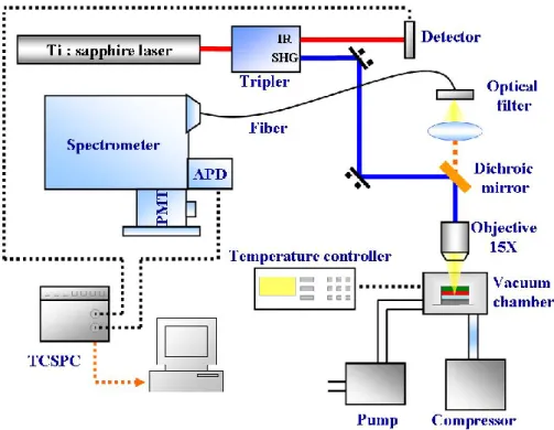
For power dependent photoluminescence (PL) system in this research, the laser source is the femto-second pulse Ti:sapphire laser. The Ti:sapphire crystal pumped by 532 nm green light laser and the output laser was so called Ti:sapphire laser, and the wavelength could be tuned around 760~820nm by adjusting the internal resonant length and gain profile. The frequency doubler crystal has been setup on the laser optical path. Finally, we can get the laser output wavelength which is about 380~410 nm for our power dependent PL measurement, this wavelength is satisfy to pump our sample for blue light region multi quantum wells (MQWs), and also this wavelength can avoid the absorption of GaN (3.4 eV) material itself and ensure most of the injected photons can reach the MQWs. The repetition rate of the laser = 76 MHz, and the spot size is about 50μm.
The tuned the 380~410 nm laser was then incident into the sample surface vertically. The sample was mounted in a closed-cycle He cryostate with a temperature controller which could be precisely controlled in the temperature region around 15 to 300 K. By the temperature controller with a set of wire heater, we could perform a serious of temperature-dependent experiments from 15 to 300 K. The luminescence signal dispersed through a 0.55-meter monochromator was detected by the photomultiplier tube (PMT). The setup detail of temperature dependent PL is shown in figure 3.2.1.
17
and non-polarized Helium-Cadmium (He-Cd) laser operated at 325 nm with the power of 35 mW. The photoluminescence spectrum from this experiment helps us to analysis the quality and optical characteristic of material. From the PL spectrum of a new compound semiconductor, we can realize the material from the related band gap. On the other hand, the PL intensity is contributed to the radiative recombination and non-radiative recombination inside the semiconductor material. Therefore, it will be a good way to understand the quality and the recombination behavior. In addition, we may analysis the PL spectrum from low temperature to room temperature to figure out the confine ability in multi hetro-junction structure.
The laser setup is show as figure 3.2.2 . The laser was reflect by three mirrors then focused by a lens with focal length was 5 cm. The laser spot was then focus to 0.1 mm in diameter. Luminescence signal emitted from the sample was collected by some lens and then the probed light was dispersed by a 0.32 monochromator (Jobin-Yvon Triax-320) with 1800, 1200, 300 grooves/mm grating and the maximum width of the entrance slit was 1 mm. In order to prevent the laser coupling with PL spectrum, we used the long pass filter in front of the entrance slit. For temperature-dependent PL measurement, all the samples were placed in the closed-cycle cryostat with temperature controller, and the experiment in our research change the temperature ranging from 20 K to 300 K.
18
Figure 3.2.1 The setup detail of Ti:sapphire laser PL system.
19
3.3 TracePro Light Tracing Simulation
Tracepro simulation is a software which is very useful and convenience for we to analysis the light field and the light extraction ability. Tracepro has been widely used in solid state lighting lens design and optoelectronic device design, this software almost cover whole simulation about light tracing issue. To simulate the ray tracing results, we should first build a model of our sample and the light sources of our structure. This software can setup different light sources and considering the reflection, scattering, absorption and bidirection scattering distribution function (BSDF) effect of the materials, then using the Monte-Carlo method to calculate the ray data from the model we build up. In our research, we simulate the extraction ability about different sample by calculate the extraction ray radiant from the active region we setup.
However, this software can't simulate the structure minor than the wavelength of the light sources we setup, this is because the calculate method of Tracepro is based on geometry optics, so it do not consider the wave optics which may appear under the sub-wavelength condition.
20
3.4 Finite-Difference Time Domain (FDTD) Simulation
Finite-difference time-domain (FDTD) is a numerical analysis technique used for modeling computational electrodynamics (finding approximate solutions to the associated system of differential equations). Since it is a time-domain method, FDTD solutions can cover a wide frequency range with a single simulation run, and treat nonlinear material properties in a natural way.
The FDTD method belongs in the general class of grid-based differential time-domain numerical modeling methods. The time-dependent Maxwell's equations (in partial differential form) are using central-difference approximations to the space and time partial derivatives. The electric field vector components in a volume of space are solved at a given instant in time; then the magnetic field vector components in the same spatial volume are solved at the next instant in time; and the process is repeated over and over again until the desired transient or steady-state electromagnetic field behavior is fully evolved.
From the introduction above, we can realize the FDTD simulation system is a good way to analysis the electric field. In LED epitaxial layer, we used FDTD to simulate the electric field distribution when electric field path through the nano structure.
21
Chapter 4 Crown-shaped Patterned Sapphire Substrate (CPSS)
In this chapter, the blue LED growth on crown-shaped PSS (CPSS) has been demonstrated. The transmission electron microscopy has been used to investigate the dislocation distribution inside the GaN epilayer. Electrical characteristic has been measured to realize the output power. We also growth the same LED structure on c-plane sapphire and hemisphere patterned sapphire, note as C-LEDs and HPSS-LEDs for comparison. Tracepro simulation results show the light extraction ability of three types of sample. At last, we simulate the optimized angle of crown-shaped PSS by Tracepro simulation software.
4.1 Fabrication of PSS and LED Devices
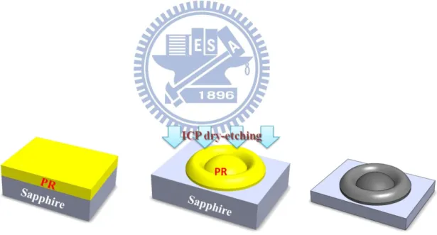
To fabricate such crown-shaped pattern sapphire substrate (PSS), we first used photolithography to defined the photo resist area and shape. Due to the limit of diffraction, two light sources will interact and performed the interference effect as Figure 4.1.1 shows. In general, if the pattern spacing of mask is too small, smaller then the wavelength of light source, the interference effect will perform by two light pass trough different pattern on the mask during the exposure process. By special design of mask, we can even get the pattern with nano-scale which broke the limit of traditional photolithography by interference effect, and this is the way how we define our photo resist. After the photo resist areas have been defined, we used Inductively Coupled Plasma (ICP) dry etching to produce our
22
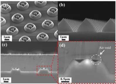
crown-shaped PSS. Figure 4.1.2 (a) shows the tilt scanning electron microscopy (SEM) image and we can clearly recognized the shaped of our pattern sapphire substrate. The diameter and interval of each crown-shaped pattern were 3 and 2 μm, respectively. The height of the cone shape was about 1.17 μm.
A standard GaN-based LED structure was then grown on the crown-shaped PSS (CPSS) and hemisphere PSS (HPSS) by a low pressure MOCVD system, denoted as CPSS-LEDs and HPSS-LEDs. The same GaN LED structure was also grown on a flat sapphire substrate as a reference, denoted as conventional LEDs (C-LEDs). During the growth, trimethylgallium
(TMGa), trimethylindium (TMIn) and ammonia (NH3) were used as gallium, indium, and
nitrogen sources, respectively. Silane (SiH4) and biscyclopentadienyl magnesium (CP2Mg)
were used as n-dopant and p-dopant source. The epitaxial structure of the GaN-based LED overgrowth which consists of 3-μm n-doped GaN (n-GaN), 10-pairs of InGaN/GaN multi-quantum wells (MQWs), and 0.2-μm p-doped GaN (p-GaN) cap layer are on all samples universal. The LED wafers were then processed into LED chips (size: 350×350μm2) and packaged in epoxy-free metal cans (TO-46). The output power of the LED was measured by an integrated sphere detector at room temperature. Figure 4.1.2 (c) shows the cross-sectional SEM image of the CPSS-LEDs. The donut-shaped air voids (n=1) were formed between the CPSS (n=1.7) and GaN (n=2.5) epilayer on top of the crown shape as shown in figure 4.1.2 (d). The hemisphere patterned sapphire substrate was fabricate for the
23
following comparison, and the cross-sectional SEM image was also been showed as figure 4.1.2 (b).
Finally, we grow the LED structure on the top of CPSS, HPSS and conventional c-plane sapphire. The epitaxial structure of the GaN-based LED which consists 3 μm n-doped GaN (n-GaN), 10 pairs of InGaN/GaN multi-quantum wells (MQWs), and 0.2-μm p-doped GaN (p-GaN) cap layer for all sample have been grow on the top of three substrates. Besides, we use the traditional LED device fabrication to define the mesa area, the p- and n- contact was then deposit by E-gun as Figure 4.1.3 shows.
24
Fig 4.1.2 SEM images for (a) tilted image of CPSS, (b) cross section of HPSS,(c) cross-sectional of CPSS-LEDs. (b) The magnified view of air avoids on top of the crown
shape.
Figure 4.1.3 LED structure growth on CPSS and the LED device with n-contact and p-contact.
25
4.2 Crystal Quality of GaN Epitaxial Layer
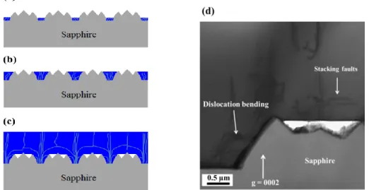
To realized the crystal quality of GaN epitaxial layer, the transmission electron microscopy (TEM) had been used. From the TEM image shows as Figure 4.2.1(d), we can clearly see the dislocation bending to the side well of the CPSS due to the epitaxial lateral overgrowth (ELOG). As the image has showed, the threading dislocation density at active region of LED will be reduced by dislocation bending. From the figure made by UCSB (Figure.4.2.2) , we realized that when the dislocation density decreased, the efficiency of LED will be improved.
For the wish to realize the growth mechanisms and the dislocation bending progress, the figure of GaN epilayer growth progress has been sketch. From Figure 4.2.1(a),(b)and (c), it shows the sketch of epitaxial lateral overgrowth mechanisms at GaN epilayer. First, the recrystallized GaN islands were grown on planar part of CPSS as shown in Figure 4.2.1(a). As GaN grew upward, there was also lateral growth toward the peak of crown. The GaN epilayer eventually grew over the crown pattern and coalesced near the summit and formed air voids between the lateral grown GaN and the crown, as shown in Figure 4.2.1(b) and Figure 4.2.1(c).
26
Figure 4.2.1 (a),(b), and (c) Schematic view of the planarization of GaN grown on CPSS; (d) TEM images of GaN grown on CPSS. Diffraction condition is g=0002.
27
4.3 Optical Characteristic of CPSS LEDs
From the transmission electron microscopy (TEM) image, we can clearly discover the dislocation bending to the side wall of the crown, as the result, we can reasonable says the crystalline quality improved by dislocation bending. Therefore, we next would like to measure the enhancement of efficiency by the lower dislocation density.
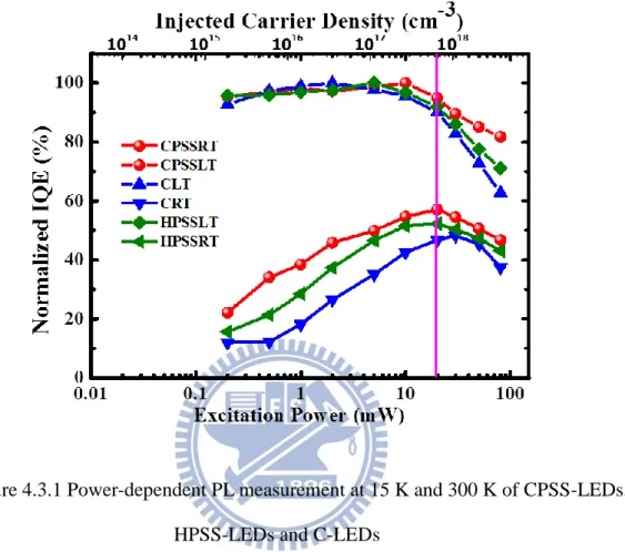
For the purpose to define the internal quantum efficiency (IQE), the power-dependent PL measurement at 15K and 300K has been used. From the relation between inject laser power and the intensity, we can fit the curve to figure out the IQE at different inject laser power. In this experiment, we ignored the non-radiative recombination at low temperature (15K), therefore, the peak at low temperature correspond to IQE equal to 100 percent.
Actually, the PL excitation intensity is difficult to estimate and it varies between different experiments. To conquer this difficulty, we can change the variable laser pumping intensity into the carrier density, which is easier to analyze and defined the IQE at operate current. The following equation shows below could transfer injected power to carrier density:
Injected carrier density
28
laser. Hence, hν should be the energy of injected photon. And the spot size of pumping laser, ϕ. The thickness of GaN and active region, dGaN and dactive, f related to the repetition rate of pumping laser, the absorption efficiency of GaN and InGaN, αGaN and αInGaN, and the
reflectance of pumping laser denote by R. From the information of Ti:sapphire laser and the lens on the optical path, we calculate the spot size ϕ = 50 µm. On the other hand, we choice dGaN = 75nm and dactive = 150nm, αInGaN = 105 cm-1, R = 0.17 and f = 76MHz to
calculate the injected carrier density in the sample. Here, we ignore the absorption of GaN due to the energy of pumping photons is less than its energy band gap.
The IQE curve fitting was then be performed as figure 4.3.1, the fitting method is defined as the collected photon numbers divided by the injected photon numbers and normalize to the maximum efficiency of low temperature (15K).
In general, we will observe the IQE at room temperature and the injection power equal to 20mW, this decision is because we actually operate LED at room temperature, and the 20mW excitation power is equal to the carrier density about 2 × 1017 cm-3 fromthe equation above, and we actually operate LED at this carrier density. Finally, we can tell the IQE enhancement of HPSS-LEDs and CPSS-LEDs is about 11 % and 21 % compared with C-LEDs. On the other hand, the CPSS-LEDs has a 9 % IQE enhancement compared with HPSS-LEDs, this results was attributed to the dislocation bending ability difference, which means the CPSS-LEDs may have lower dislocation density.
29
Figure 4.3.1 Power-dependent PL measurement at 15 K and 300 K of CPSS-LEDs, HPSS-LEDs and C-LEDs
30
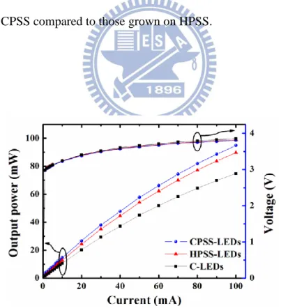
4.4 Electrical Characteristic of CPSS-LEDs
The 350 × 350 μm2 LED device has been fabricated to investigate the electrical characteristic. The power-current-voltage (L-I-V) relation have been measured and shown as Figure 4.4.1. The L-I-V curves displays the typical characteristics of three samples. With an injection current of 20 mA, the forward voltages are 3.4、3.39 and 3.38 V, and the output powers are 20.2 mW, 24.3 mW and 26.7 mW, for C-LEDs, HPSS-LEDs and CPSS-LEDs, respectively. As compared with C-LEDs, the output power of HPSS-LEDs and CPSS-LEDs were enhanced by 20% and 32.1%.
we assume the light output enhancement can be attributed to following factors: First, the threading dislocation density (TDDs) were reduced by the ELOG process, enhanced the crystal quality of active region. The non-radiative center decrease and so do the non-radiative recombination, and the photon generation efficiency increased reasonably. This results is similar to those reported before, such as GaN grown on recess-patterned PSS by D.S. Wuu et.al. [35]. Secondly, more lights can be extracted from the LEDs because of the light scattering effect from the air voids on the crown tops. It has been reported that the inclined facets of PSS can redirect photons back to the device surfaces and leads to higher light extraction efficiency [36]. In addition, the LEDs on CPSS exhibited higher output power than on HPSS. This is due to embedded donut-shaped air voids formed between PSS and GaN epilayer. The reason why donut-shaped air voids enhance the light output power
31
can be explain from Snell's law:
where n1 is the reflective index of incident medium, θ 1 is the incident angle, n2 is the
reflective index of output medium andθ 2 is the refractive angle. This equation shows it can
reach total reflective angle easier when the different between n1 and n2 get lager, this means
it has better reflective ability. As we know, the reflective index of air, sapphire and GaN is 1, 1.7 and 2.45, respectively.
According to the result, there is an additional 9.8% output power enhancement for the LEDs grown the CPSS compared to those grown on HPSS.
32
4.5 TracePro Simulation Results of Crown-shaped PSS LED
Although the L-I-V curve and the Snell's law shows the enhancement and given an
physical meaning to explain the enhancement by air voids, we still would like to find out the better physical understanding to figure out the how the photon emitting from the MQWs act inside the LEDs. Tracepro simulation which based on Monte Carlo method seems to be a great solution to reach our purpose. The wavelength used in simulation is 450 nm, and the total power emitting from MQWs is 10mW for 10000 light rays were assumed to be isotropically emitted and monochromatic unpolarized. In this Monte Carlo calculation we don't consider the dislocation, we setup the same data of each layer for three samples. And we don't consider the effects of electrical pad and current spreading, either. This means the results will only shows the effect caused by patterned shaped (flat, hemisphere and crown) and air voids. The simulated illuminance maps of three LED samples are shown in figure 4.5.1. As it can be seen in the figures, the maximum candelas values in three maps were 3.57, 5.41 and 5.69 mW/sr for C-LEDs, HPSS-LEDs and CPSS-LEDs, respectively. The simulation results of output enhancement have been made as table 4.4.1. It indicates that more photons escape out into the air easier in CPSS-LEDs than in C-LEDs and HPSS-LEDs. The simulation results clearly show the light extraction efficiency enhanced by patterned sapphire substrate due to the light scattering effect. So far, we have simulated the light extraction ability about different substrate and now we would like to further optimize the
33
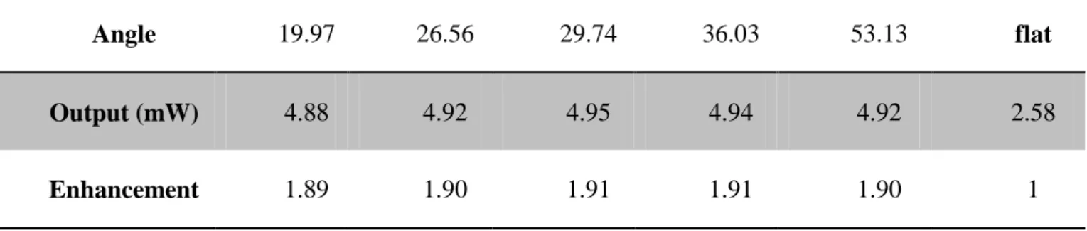
CPSS-LEDs. To reach this purpose, we change the simulation model of crown-shaped patterned of different crater angle. In addition, a smaller angle indicates the steep slope with greater depth in the crater, whereas, a larger angle implies a slant slope from the edge of the crater. We used the same simulation parameter as above and show the simulation results as Figure 4.5.2. The light extraction efficiency of total radiant flux (LEE_TRF) considers the rays that escaped from every surface of the LEDs. In addition, a smaller angle indicates the steep slope with greater depth in the crater, whereas, a larger angle implies a slant slope from the edge of the crater. From the angle-dependent results, we figure out the optimization angle is between 30 degree to 35 degree. The simulation results of output enhancement have been made as table 4.5.2.
34
Figure 4.5.1 Tracepro simulation of candela map taken from InGaN LEDs grown on (a) C-LEDs, (b) HPSS-LEDs and (c) CPSS-LEDs
Table 4.5.1 Light extraction Tracepro results of C-LED, HPSS-LED and CPSS-LED.
Model C-LED HPSS-LED CPSS-LED
35
Figure 4.5.2 Optical properties as function of crater angle for the crown-shaped patterned. The insert shows crater of CPSS.
Table 4.5.2 Angle dependent Tracepro simulation optimize results of CPSS-LEDs.
Angle 19.97 26.56 29.74 36.03 53.13 flat
Output (mW) 4.88 4.92 4.95 4.94 4.92 2.58
36
Chapter 5 Enhanced Light Output Power by Nanorods Template
The high performance GaN-based light-emitting diodes (LEDs) with embedded microscale air voids and an SiO2 nanomask by metal–organic chemical vapor deposition
(MOCVD) were demonstrated. Microscale air voids and an SiO2 nanomask were clearly
observed at the interface between GaN nanorods (NRs) and the overgrown GaN layer by scanning electron microscopy (SEM). Atomic force microscopy (AFM) image shows the re-growth un-doped GaN are flat enough to growth LED structure on top of it. From the reflectance spectra we show strong reflectance differences due to the different refractive index gradient between the GaN grown on the nanorod template and sapphire. It can increase the light extraction efficiency due to additional light scattering. The transmission electron microscopy (TEM) images show the threading dislocations were suppressed by nanoscale epitaxial lateral overgrowth (NELOG). The LEDs with embedded microscale air voids and an SiO2 nanomask exhibit smaller reverse-bias current and large enhancement of
the light output (65% at 20 mA) compared with conventional LEDs. Finally, the finite difference time domain (FDTD) simulation has been used to reveal that the light extraction enhancement by microscale air void.
37
5.1 Fabrication of Gallium Nitride Nanorods Template
The method of fabricate the GaN nanorods template is shows as followed. First, we grew 2μm un-doped GaN epitaxial layer on the c-plane sapphire substrate by metal-organic
chemical vapor depositions (MOCVD). Next, we deposited 10 nm thick Ni and 200 nm thick SiO2 layer on the top of 2μm un-doped GaN surface by E-gun evaporator and
plasma-enhanced chemical vapor deposition (PECVD). Followed by annealing process, we use rapid thermal annealing (RTA) to form self-assembled Ni clusters with a following nitrogen gas at 850°C for 1 minute. We treat these Ni clusters by Ni nano-mask. After that, the dry etching process was employed to form SiO2 nanorods and un-doped GaN nanorods
by reactive ion etching (RIE) and inductive coupled plasma (ICP). The RIE and ICP powers are 100 W. We used RIE for 3 minutes long to formed SiO2 nanorods on the top of un-doped
GaN, and then we treat SiO2 nanorods as followed mask of ICP. Next, we used the ICP
system for 34 minutes, and the etching condition were describe as followed. The etching gases were mixture of Cl2 (5 sccm) and Ar (50 sccm), and the etching rate is about 58 nm
per minute. The sketch of fabrication flow was showed as Figure 5.1.1. Finally, we fabricate the 2μm GaN nanorods with 200 nm SiO2 nanomask, named as nanorods (NRs) template,
the nanorods density was around 3.3 х 108
cm-2 and the diameter of nanorods is from 250 to 500 nm as shown in Figure 5.1.2.
38
our GaN template. this growth process adding an extra m-plane (1010) GaN on the side walls of the etched pillars and inclined r-plane facets (1102) close to the top of the nanorods[37]. Due to the different growth rate between m-plane and r-plane, the microscale air voids formed. Frajtag et al have also reported that the semipolar planes coalesce first due to their higher growth rates relative to the growth rates on the nonpolar side faces of nanowires [38]. The final step consists of planar epitaxial GaN overgrowth, and air voids and SiO2 nanomasks
were encapsulated as shown in figure 5.1.3. All of these growth mechanisms help the formation of air voids between nanorods. The sketch of re-growth process has been showed as Figure 5.1.3. From the cross-sectional scanning electron microscopy (SEM) image of re-growth un-doped GaN layer as shown as Figure 5.1.4, we can clearly recognized the microscale air voids embedded between nanorods.
During the growth process, the trimethylgallium (TMGa), trimethylindium (TMIn) and ammonia (NH3) were used as gallium, indium and nitrogen sources. From the cross-section
SEM, we can clearly see the whole epitaxial layer including the micro-scale air voids. For the purpose to make sure the morphology of un-doped GaN surface, the atomic force microscopy
(AFM) measurement has been used and showed as Figure 5.1.5. And compared with un-doped GaN growth on c-plane sapphire, the un-doped GaN growth on GaN nanorods even showed lower root mean square (RMS) of roughness. The roughness RMS roughness of un-doped GaN growth on nanorods is about 0.804 nm and the roughness RMS of un-doped
39
GaN growth on c-plane sapphire is about 1.012 nm, respectively. This surface morphology is good enough for we re-growth the LED structure on it. The epitaxial structure of the GaN-based LED overgrowth on GaN NRs template consist 3 μm n-doped GaN (n-GaN), 10-pairs InGaN/GaN multi-quantum wells (MQWs), and 0.2 μm p-doped GaN (p-GaN) cap layer. We use the traditional LED device fabrication to defined the mesa area, the p- and n- contact was then deposit by E-gun as Figure 5.1.6 shows.
40
Figure 5.1.2 (a) Cross-section and (b) tilted SEM of GaN nanorods.
41
Figure 5.1.3 Sketch of NELOG process
42
Fig 5.1.5 AFM image of (a) u-GaN on nanorods, (b) u-GaN on sapphire
(a)
43
Figure 5.1.6 LED structure growth on nanorods template and the LED device with n-contact and p-contact.
44
5.2 Crystal Quality of Bulk GaN Epitaxial Layer
For the purpose of realizing the crystal quality of bulk GaN film, the Raman measurement and the transmission electron microscopy (TEM) measurement had been used.
In general, the GaN growth on c-plane sapphire suffer from the huge strain due to the lattice mismatch (about 15% difference) between GaN and sapphire substrate. Therefore, the research of strain relaxation is very important, the first step is to calculate the strain and define the strain in GPa as a pressure unit.
Raman backscattering measurement is a good solution to investigate the residual strain of GaN epitaxial layers, and for the purpose to analyze the strain in the GaN films, the Raman spectrum had been measured as Figure 5.1.1. The Raman spectrum shows the E2
high peak of both un-doped GaN growth on NR template and growth on standard low temperature GaN. The result shows that the E2 high peak is about 568.5 cm-1 of our
un-doped GaN growth on NR template and 570.4 cm-1 of un-doped GaN growth on general c-plane template. As we know, the E2 high peak of strain free GaN is 566.5 cm-1. This
spectrum is helpful for we to analyzed the residual stress in the GaN film, if the peak from Raman spectrum is larger than strain free GaN, we can said that it suffer from compressive stress, and the lager peak shift contribute to the lager stress affect in GaN film. Besides, we can calculate the actual stress on GaN by the following equation:
45
where the Δω is the peak shift between strain free GaN epi-layer and the strained GaN epi-layer, ω0 is the peak of strain free GaN epi-layer, and ωE2 is the peak of strained GaN
epi-layer; C is the biaxial strain coefficient, which is 2.25 cm-1/GPa and σ is the in-plane stress which we want to calculate.
According to the equation, we can calculate the compressive stress σ of both sample is about 1.33 GPa and 0.44 GPa. This result also shows that we can reduced the stress successfully by using nanorods technique.
On the other hand, when we consider the crystal quality, we first talk about dislocation. From TEM image show as Figure 5.2.2, we can clearly investigate the dislocation bending into the air voids. Due to the dislocation bending, the dislocation density can successfully reduce, and compared with general GaN growth on c-plane sapphire the dislocation density reduce from 108~109 cm-2 to 5×107 cm-2. And we can also say that the air voids and SiO2
induced by lateral overgrowth between GaN NRs could be regarded as dislocation bending channel.
From the results, we inference the quality improve by following reasons, strain relaxation by GaN nanorods template and ELOG process lead to dislocation bending. This phenomenon caused the weaker quantum-confined Stark effect (QCSE).
46
Figure 5.2.1 Raman spectrum of E2 high peak
47
5.3 Observation of Dislocation in GaN epitaxial layer
In this section, the TEM image has been employed to investigate the crystal quality and the dislocation distribution of our GaN nanorods template. From the TEM image, we can clearly see the dislocation bending to the micro scales air voids. On the other hand, the SiO2 which we treat it as nano-mask can also stop the dislocations.
In general, we can recognize the threading dislocation in to three types, edge, screw, and mixed dislocations. From the cross-section TEM image, three types of dislocations in our nanorods template can be observed clearly.
In order to investigate the kind of threading dislocation, the cross-sectional dark-field TEM images were measured as shown in figure 5.3.1. In general, under g=1100 two-beam conditions, the edge and mixed dislocations were visible, and under g=0002 two-beam conditions, the screw and mixed dislocations can be observed [39]. From cross-sectional TEM images (figures 5.3.1(a) and (b)), we can define clearly the types of threading dislocation. On the other hand, we found that the fewer screw dislocations are observable on the top of SiO2
nanorods and most of the edge and mix dislocations were bending near voids as shown in the enlarged images of region I and region II as shown in figures 3(c) and (d), respectively. Thus, the TDDs were reduced effectively by the NELOG method.
TEM image prove the inference we predict, the NELOG process lead to micro-scale air voids and dislocation bending. On the other hand, the SiO2 nano-mask blocked the screw
48
threading dislocation. Both phenomenon could reduce the dislocations in MQW, therefore, the crystal quality will be improved.
49
Figure 5.3.1 Cross-sectional TEM images of GaN epilayer overgrown on GaN NRs template (a) under two-beam condition for g D 1N100, (b) under two-beam condition for g D
50
5.4 Optical Characteristic of Nanorods LED
In order to investigate the internal quantum efficiency (IQE) of our nanorods LED (NR-LED), the PL internal quantum efficiency measurement have been used. Figure 5.4.1 shows the curve related to injected laser power at 15 K and 300 K. The general conventional LED (C-LED) was also measured for comparison. In this experiment, we ignored the non-radiative recombination at low temperature (15K), therefore, the peak at low temperature correspond to IQE equal to 100 percent.
Actually, the PL excitation intensity is difficult to estimate and it varies between different experiments. To conquer this difficulty, we can change the variable laser pumping intensity into the carrier density, which is easier to analyze and defined the IQE at operate current. The following equation shows below could transfer injected power to carrier density:
Injected carrier density
(5-1)
Where P is the power of pumping laser, h is the Planck constant, ν is the frequency of laser. Hence, hν should be the energy of injected photon. And the spot size of pumping laser, ϕ. The thickness of GaN and active region, dGaN and dactive, f related to the repetition rate of
51
reflectance of pumping laser denote by R. From the information of Ti:sapphire laser and the lens on the optical path, we calculate the spot size ϕ = 50 µm. On the other hand, we choice dGaN = 75nm and dactive = 150nm, αInGaN = 105 cm-1, R = 0.17 and f = 76MHz to calculate the
injected carrier density in the sample. Here, we ignore the absorption of GaN due to the energy of pumping photons is less than its energy band gap.
The IQE curve fitting in this experiment is defined as the collected photon numbers divided by the injected photon numbers and normalized to the maximum efficiency of low temperature. For the LED grown on planar sapphire substrate and GaN nano-pillar template, one could clearly see that the IQE increased with injected carrier density increased to reach its maximum and decreased as the injected carrier density further increased. The tendency of this two efficiency curves at 15 K and 300 K was quite similar. But under low injection carrier density range, the IQE at 300 K increased more pronounced than it at 15 K. The corresponding density to the peak efficiency for the LED grown on planar sapphire (46%) in 300 K is at injected carrier density of about 1018 cm-3, which is larger than it at 15 K, about 4×1016 cm-3. On the other hand, for the LED grown on GaN nano-pillar template, a similar dependence of the IQE on the injected carrier density was observed. Nevertheless, in term of the peak efficiency (53%) in 300 K at injected carrier density of 2×1017 cm-3.
From the curve we fit by experiment data, it shows the IQE of C-LEDs and NR-LEDs is 46% and 53%, respectively. This result shows the IQE enhancement is 1.15 times compared
52
with C-LEDs by using nanorods template at 20mW excitation power. The reason we choice the IQE under 20mW excitation power is because of the corresponding carrier density is about 2 × 1017 cm-3 , this carrier density value is close to the LED devices operate at 20 mA.
All the information provided above could be the evidence to explain the origin of higher IQE for the LED grown on nanorods template. Here, we collected the temperature dependent PL intensity and plot the normalized intensity with inversed temperature which is understood as Arrhenius plot in figure 5.4.2. Then, this temperature dependent curve could be fitted by the following equation to get the activation energy:
IT = I0 / [1+A exp(-Ea / kT)+B exp(-Eb / kT)] (5-2)
Where IT, I0 are the integrated PL intensity for T and 0 K, A and B are constants, k is the
Boltzmann constant, T is the temperature, Ea is the activation energy for PL quenching, and Eb is generally associated to the free exciton binding energy [40]. The experiment data was
then fitting by the equation above, and the activation energy (Ea) of LED growth on nanorods
template and c-plane sapphire are 67 meV and 61 meV, respectively. The physical meaning of activation energy can be explained by the ability to confine the carriers within the potential minima, which means the Ea corresponding to the confinement of quantum well. It had been