國
立
交
通
大
學
電子物理研究所
博 士 論 文
運用掃描式探針微影技術研發製作矽質奈米元件結構
Silicon nanofabrication with scanning probe lithography technique
研 究 生:吳家豪
指導教授:許鉦宗 教授
趙天生 教授
運用掃描式探針微影技術研發製作矽質奈米元件結構
Silicon nanofabrication with scanning probe lithography technique
研 究 生:吳家豪 Student:Chia-Hao Wu
指導教授:許鉦宗 Advisor:Jeng-Tzong Sheu
趙天生 Advisor:Tien-Sheng Chao
國立交通大學
電子物理研究所
博 士 論 文
A ThesisSubmitted to Institute of Electrophysics College of Science
National Chiao Tung University in Partial Fulfillment of the Requirements
for the Degree of Doctor of Philosophy
in Electrophysics
June 2007
Hsinchu, Taiwan, Republic of China
運用掃描式探針微影技術研發製作矽質奈米元件結構
學生:吳家豪
指導教授:許鉦宗 博士
趙天生 博士
國立交通大學
電子物理研究所 博士班
摘
要
『奈米科技』已然成為全世界科技發展的重點之一,它亦將引發本世紀在材料、 生化、光電、能源等等技術的革命,人類將可從此一先進研發科技中獲得豐碩的實際 效益。近年來,奈米科技製程技術的研發受到許多研究團隊的高度重視,其中包含了 發展製造奈米級元件結構的先進製作技術,以及設計研究開發新穎的奈米結構以因應 未來前瞻性的領域應用。在眾多先進的微影技術當中,例如:電子束微影技術(EBL), X 光微影技術(XRL),以及掃描式探針微影技術(SPL)等技術,其中又以掃描式探 針微影技術最具有製造奈米結構元件的潛力,因為此一先進微影技術不僅可應用於奈 米尺度下將試片表面的特性轉變改質,並且可應用於製造生產所需的奈米級元件結 構。掃描式探針微影技術乃是利用探針接近試片表面的時候,利用外加的電場誘發局 部陽極氧化試片(抑或者是利用探針針尖的穿邃電流,來致使試片表面化學官能基分 子層結構特性改質),來製備奈米級元件結構。此種微影技術具有較高的解析度、精 確的對準特性、以及可靠度高,也沒有一般微影的輻射熱損害,再加上製作簡易而且 有著較低成本等等的優勢。本論文研究也將利用原子力顯微鏡掃描式探針沾附有機分 子溶液,並藉由空氣中水分子當媒介,直接在矽質試片上進行奈米級分子層結構圖案
我們可以藉由此方式來塗佈製造出小於 100 奈米解析度的各式化學官能基分子層結 構圖案。因此,掃描式探針微影技術被視為發展奈米元件的前瞻關鍵技術。在本論文 研究,我們在一維的矽質奈米導線上選擇性沈積金奈米粒子,並且將其應用於生物分 子及相關的化學物質的感測研究,並將此一前瞻性的技術平台建構完成。矽質奈米導 線乃是利用掃描式探針微影技術並結合非等向式四-甲基-氫氧化氨 (TMAH) 濕式蝕 刻 (或 RIE 乾式蝕刻)來完成的。而 15 奈米粒徑大小的金奈米粒子乃是利用化學鹽類 還原的方式來製備的。然後,我們結合運用掃描式探針微影技術與自我組裝分子層技 術在矽質奈米導線的表面進行金奈米粒子的選擇性沈積。我們使用已沾附了 2-胺基-乙基-3 胺基丙烷三甲氧基矽化合物(AEAPTMS) 有機分子的掃描式探針,並藉由空氣 中的水膜分子當作有機分子傳遞擴散的媒介,然後在矽質奈米導線上圖佈沈積有機分 子層薄膜,當胺基的有機團修飾在矽質導線表面上時,便會使得矽質導線表面產生帶 正離子的矽烷化改質效應。此外,本論文研究也成功地利用掃描式探針微影技術在二 氧化矽表面利用 AFM 探針針尖的穿邃電流來致使試片表面 2-胺基乙基-3 胺基丙烷 三甲氧基矽化合物(AEAPTMS)化學官能基有機分子層鍵結產生斷鍵而使試片表面改 質。然後,藉由庫倫力的吸引作用,而與帶負電的金奈米粒子產生靜電吸附而沈積鍵 結在矽質奈米導線上的矽烷化改質結構區域。我們深信此一前瞻性奈米製造技術藉由 結合掃描式探針微影技術與自我組裝分子層技術所研發製造出的奈米結構元件,未來 將可廣泛地應用於奈米電子元件與奈米生醫感測元件的研究領域,無論在學術及工業 技術研究上皆極具價值。更重要的一點,本研究對於未來奈米級的電子元件製程技術 的研發上,提供了一套操作容易且成本低廉的奈米元件製程研發技術。
Silicon nanofabrication with scanning probe lithography technique
Student:Chia-Hao Wu
Advisors:Dr. Jeng-Tzong Sheu
Dr. Tien-Sheng Chao
Institute of Electrophysics
National Chiao Tung University
ABSTRACT
One of the focal points that “nanotechnology” has already become development in science and technology of whole world. It will also cause the revolution in the technology, such as material, biochemistry, photo electricity, energy, etc. in this century. Mankind can obtain the actual benefit from this advanced nanotechnology. Recently, it is more interesting in research on nanotechnology, which includes the development of advanced manufacturing skills for fabricating nanometer size devices and the design and research of new nanometer structures for novel applications. Among these advanced lithography techniques, such as electron beam lithography, x-ray lithography and scanning probe lithography (SPL), etc., one potential approach for fabricating the nanostructures is the use of scanning probe lithography. SPL techniques have been used to perform nano-scaled surface modification, and dominated the research field of nano-structures fabrication. SPL, employing a conductive probe to induce electric-field-enhanced local anodic oxidation (or tunneling currents enhanced the surface modification of chemical functionality), provide its advantages of high resolution, alignment accuracy, high reliability, absence of radiation damage, simpler and lower-cost. We also utilize the AFM scanning tip as a “pen” to transport an “ink” containing organic molecules onto a substrate surface via a water meniscus to write nano structures and subsequently read patterns, it is possible to create nano-scale patterns with remarkable resolution (<100 nm) and simultaneously control the
chemical functionality of the written regions. This makes SPL a unique tool that has been considered as a crucial technology for nanometer scale structures.
In this research, we propose a novel platform based on one-dimensional silicon nano-wires (SiNWs) and gold nano-particles for detection of the biological molecular and chemical species. SiNWs were performed based on SPL technique and anisotropic tetra-methyl-ammonium hydroxide (TMAH) wet etching (or RIE dry etching). Gold nano-particles were obtained by chemical reduction methods, and the diameter size of gold nano-particles was controlled by the reaction time. Then, we will utilize a combination of scanning probe nanolithography and self-assembly monolayer (SAMs) techniques for realizing selective deposition of gold nanoparticles onto the SiNWs surface. AFM scanning tip was adopted to deposit organic N-(2-aminoethyl)-3-amino-propyl-tri-methoxysilane (AEAPTMS) molecules nanopatterns through a water meniscus onto the SiNWs surface. In addition, selective patterning of self-assembled AEAPTMS monolayer on the thin SiO2
surface of SiNWs is realized by using SPL local filed-induced bond breaking technique. Afterwards, amino silane molecules modification as linkers for selectively anchoring gold nano-particles onto silanation modification patterns on the SiNWs surface via Coulomb force. It is believed that the proposed nanofabrication technique combined SPL method with the SAMs process can be further applied in both nano-electronics and nano-biochemical sensors applications.
誌
謝
本研究論文得以順利完成,首先由衷的感謝交大奈米科技研究所教授許鉦宗博士 以及交大電子物理所教授趙天生博士兩位指導教授多年來的關心照顧、悉心指導與啟 發,使得作者在專業領域上受益良多,得以能夠順利地在職進修完成博士學位。 研究期間,由衷感謝國家同步輻射中心(NSRRC)梁耕三主任、陳家浩博士、 人 事 趙 平 文 先 生 以 及 臺 灣 師 範 大 學 化 學 系 洪 偉 修 教 授 等 人 的 關 心 、 協 助 與 幫 忙,加上國家奈米米元件實驗室(NDL)、交大奈米中心(SRC)所提供之完善優良 的製程設備,使本人得以順利完成此研究論文。此外,感謝交大電子所文政學 長、建豪學長、柏儀同學,電物所偉成學弟等人在實驗上提供許多寶貴的意見, 也要感謝實驗室的諸多伙伴們:振嘉、柏鈞、泰瑞、皓恆、宥任、裕得、玠澤、 學宏、振廷、錫波、奕貞、欣霖、子訓、昶龍等學弟的在實驗上的諸多幫忙與 協助,在此一並致上誠摯的感激與謝意。 最後,謹以此一研究論文獻給我最敬愛的父母及家人。衷心感謝我最敬愛的父母 以及兄、姐,感謝您們多年的提攜關心、鼓勵與幫助,同時也感謝愛妻碧琪與寶貝女 兒芷瑀於求學期間給予我的關心與鼓勵,在您們的支持與肯定下,使得我能全力以赴 順利完成學業。 吳家豪 於交通大學 June 25, 2007
Contents
Chinese abstract ……… i
English abstract ……… iii
Acknowledgement ……… v
Contents ……… vi
Figure Captions ……… ix
1. Introduction ……… 1
1.1 Interesting nano-monde……… 1
1.2 Ultimate resolution limit of optical lithography……… 4
1.3 Introduction of next generation lithographies (NGLs) ……… 4
1.3.1 Electron-beam lithography (EBL) ……… 5
1.3.2 Focused ion beam lithography (FIB Litho) ……… 5
1.3.3 Extreme ultraviolet lithography (EUV Litho) ……… 5
1.3.4 X-ray lithography (XRL) ……… 6
1.3.5 Micro contact printing (μCP)……… 7
1.3.6 Scanning probe lithography (SPL) ……… 7
1.4 Organization of this dissertation ……… 8
Reference ……… 10
2. Scanning Probe Nanolithography ……… 13
2.1 The history of SPM invention ……… 13
2.2 General principle of scanning probe microscopy (SPM). ……… 15
2.3 The mechanism of SPL field-induced local oxidation ……… 19
2.4 Orientation-dependent anisotropic wet Etching……… 21
2.5 Influenced parameters of SPL field-induced oxidation ……… 23
2.5.1 Additional bias effect between tip and sample surface ……… 23
2.5.2 SPM tip force effect between tip and sample surface ……… 26
2.5.3 Effect of APM-tip scanning speed……… 27
2.5.4 Influence of ambient humidity ……… 28
2.6 Nano filter structures fabrication on (100)-Si substrate by suing SPL
method ……… 31
2.7 Linearity control of Scanning Probe Lithography on (110) Silicon Subatrate……… 32
2.7.1 Linearity control experiment ……… 33
2.7.2 Linear control of nanostructures transfer ……… 34
2.8 Summary ……… 41
Reference ……… 42
3. Dip-Pen Nanolithography ……… 44
3.1 Introduction of dip-pen lithography applications.……… 45
3.2 Impact of UV-induced production of gold nanoclusters on the SiO2 Surface of SiNWs by using DPN technique ……… 47
3.2.1 Experiment details of the UV-induced production of gold nano- clusters with DPN lithography ……… 48
3.2.2 Relationship of DPN Transport Mechanisms ……… 49
3.2.3 X-ray photoelectron spectra of UV-induced reduction of gold nanoclusters ……… 50
3.2.4 Electrical characteristics of influence of UV-induced reduction of gold nanoclusters. ……… 55
3.3 Selective deposition of gold particles on Dip-pen Nanolithography patterns on silicon dioxide surfaces. ……… 57
3.3.1 Generate the molecular monolayer by DPN technique ……… 57
3.3.2 Colloidal gold nano particles synthesis and anchored onto the amino-terminal surface with the self-assembly method (SAMs) …… 59
3.3.3 Linear control patterning of the DPN lithography……… 61
3.4 Gold nanoparticles selective anchored on DPN AEAPTMS regions 64 3.5 Conclusions ……… 67
Reference ……… 68
4. Low Electron Energies of Scanning Probe Electric-filed-induced Bond Breaking Lithography. ……… 71
4.1 The invention review of low-dimensional novel patterning.………… 71
4.2 Experimental details of SPL bond breaking patterning of amino- silanation modified SiO2 surface ……… 74
4.3 Efficiency of SPL bond breaking with selective deposition.………… 76
4.4 The mechanism of SPL field-induced bond breaking. ……… 78
4.5 Low-dimensional patterning by using SPL bond breaking. ………… 83
4.6 Interesting of SPL electric-filed induced gray-level selective patterning……… 88
4.7 Gold nanoparticles selective anchored locally on SiNWs by using SPL bond breaking technique. ……… 94
4.7.1 Modification of channel surface of silicon nanowires. ……… 96
4.7.2 Electrical characteristic analysis of various modified P-SiNWs. .…… 98
4.8 Photoresponse of surface plasmon resonance of SiNWs with desired gold nanoparticles.……… 101
4.8.1 Physical principles of surface plasmon resonance. ……… 102
4.8.2 Small amount of gold nanoparticles was controllable to selective anchored on the desired p-channel surface of SiNWs devices.……… 104
4.8.3 Photoconductivity with p-channel of SiNWs with few amounts of AuNPs is enhanced by surface plasmon resonance. ……… 107
4.9 Conclusions .……… 112
Reference ……… 113
5. Summary ……… 116
Appendix Autobiography ……… 118
Figure Captions
Figure 1.1 IBM Millipede nanomechanical data storage systems. This system makes it possible to reach speeds of read/write of several Mbits/sec, and makes it possible to reach densities of 153 Gbits/in².……… 2 Figure 1.2 The Semiconductor Industry Association’s 2006 national technology
roadmap for memory technologies and associated with the lithographic technologies that critical dimensions. ……… 3 Figure 2.1 Principle of operation of the scanning tunneling microscope from the
original article on the STM. The piezodrives Px and Pyscan the metal
tip M to traverse the surface. It describes the operation of the microscope for purpose tunnel effect. ……… 14 Figure 2.2 The schematic of the position-sensitive photo detector (PSPD) …… 16 Figure 2.3 The relationship curves of interatomic force vs. distance between
SPM tip and sample surface. ……… 17 Figure 2.4 Distribution diagram of electric field exists between the apex of
AFM-tip and the substrate surface. ……… 19 Figure 2.5 Schematic principle of SPM-based electric-field induced local
oxidation process. ……… 21 Figure 2.6 Diagram of orientation-dependent anisotropic wet etching in various
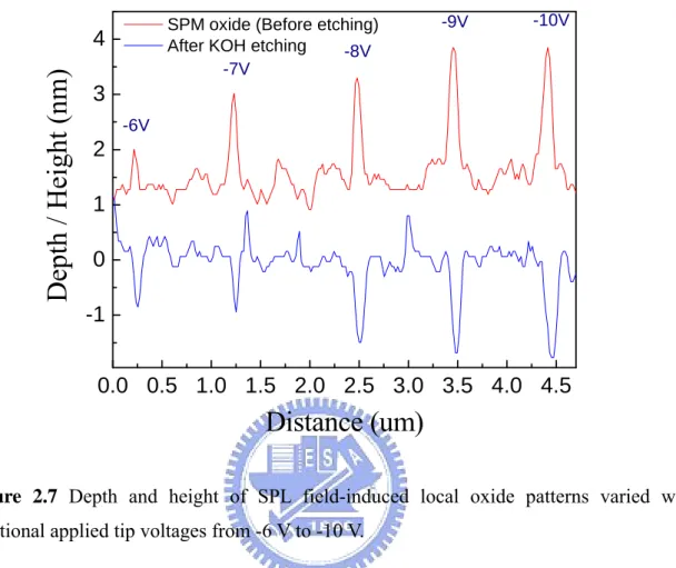
orientation silicon planes. (a) (100) crystallographic plane, (b) (110)- crystallographic plane. ……… 22 Figure 2.7 Depth and height of SPL field-induced local oxide patterns varied
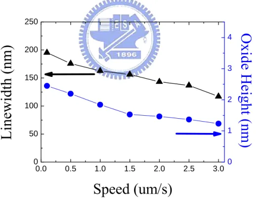
with additional applied tip voltages from -6 V to -10 V. ……… 24 Figure 2.8 Chacteristics curve of linewidth and oxide height of SPL
field-induced local oxide patterns varied with different tip voltages from -5 V to -10 V. ……… 25 Figure 2.9 Tip force characteristics curve of local oxidation grid lines. The tip
bias, tip scanning speed, and ambient humidity were maintained on -9 V, 1.0 μm/sec, and 45 ± 1%, respectively. .……… 26
Figure 2.10 Characteristic curves of oxidation grid lines of effect of scanning speed. The tip bias, tip force, and ambient humidity were maintained on -9 V, 15 nN, and 45 ± 1%, respectively. ……… 27 Figure 2.11 Characteristic curves of oxidation grid lines of influence of ambient
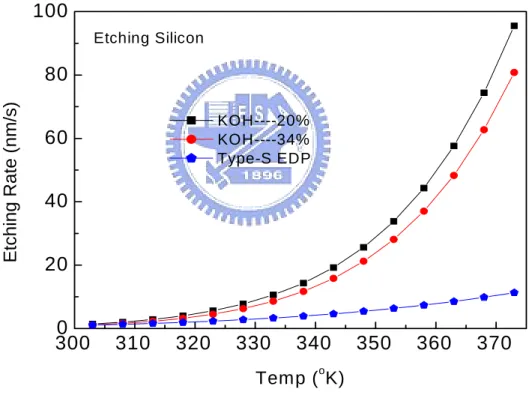
humidity. The tip bias, tip force, and scanning speed were maintained on -9 V, 10 nN, and 1.0 μm/sec, respectively. .………… 28 Figure 2.12 Characteristic relationship curves of etching rate vs. etching
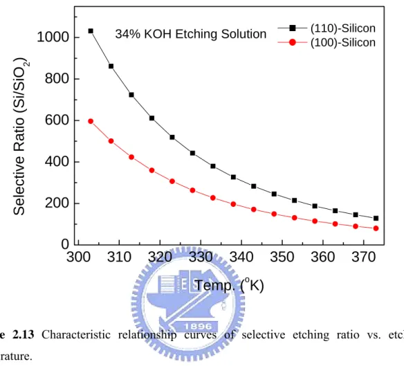
temperature. ……… 29 Figure 2.13 Characteristic relationship curves of selective etching ratio vs.
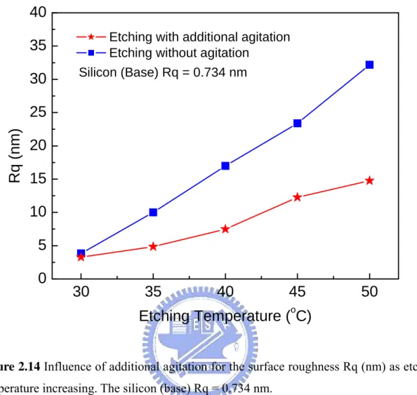
etching temperature. ……… 30 Figure 2.14 Influence of additional agitation for the surface roughness Rq (nm)
as etching temperature increasing. ……… 31 Figure 2.15 SEM images of nano-filter structures. ……… 32 Figure 2.16 Nanostructure grid line patterns transfer on (110)-Si procedure by
using the multipixel scanning method of scanning probe lithography. 34 Figure 2.17 AFM topographic height profiles along the local oxidation
nanostructure grid line marked patterns by utilizing the multipixel scanning times and different line/space of the pitch. (a) Pitch = 40 nm ; (b) Pitch = 30 nm. ……… 36 Figure 2.18 Linear control of pattern transfer of line nanostructure into (110)
silicon substrate by SPM-based multipixel scanning local oxidation and wet etching in a 34 % KOH solution for 45 sec.……… 37 Figure 2.19 Linearity characteristic curve of oxidation patterns transfer into
(110)-silicon wafer by using the scanning probe lithography technique after aqueous KOH anisotropic wet etching process. The pitch of between each scanning pixel is 15 nm……… 38 Figure 2.20 Nanostructure pattern Gauss distribution illustration of transferred
grid line nanostructure into (110) silicon wafer by the scanning probe lithography and anisotropic wet etching. (a) one pixel patterning; (b) two pixels patterning; (c) three pixels patterning; (d) four pixels pattering. The average linewidth is around 25.88 nm, 44.47 nm, 64.41 nm, and 77.76 nm, respectively. ……… 39
Figure 2.21 SEM image of the high aspect ratio (9.71 : 1) Si nanostructure fabricated by SPM-based local oxidation and wet anisotropic etching. The pattern height is about 191.2 nm and the pattern width is about 19.69 nm. ……… 40 Figure 3.1 Schematic representation of Dip-Pen Nanolithography (DPN).
Transport mechanism of molecules to the surface via the water meniscus forms between the AFM-tip and the sample surface in air. 44 Figure 3.2 Characteristic curve between speed of the dip-pen lithography and
relative humidity of environment at room temperature. ……… 49 Figure 3.3 X-ray photoelectron spectroscopy (XPS) analysis spectra of the 365
nm UV-light irradiation process on the SiO2 surface of the silicon
substrate. ……… 51 Figure 3.4 (a) Schematic diagram of the Dip-Pen Nanolithography directly
patterning. (b)AFM images of a silicon nanowire device on (100) SOI substrate fabricated by using scanning probe microscope (SPM) local oxidation method and TMAH wet etching. Nanowire is about 100 nm wide and 2 μm long. ……… 52 Figure 3.5 XPS spectra of the AuCl- / native oxide / Si system as function of UV
exposure time. It was found that UV irradiation induced production of gold nanoclusters on the surface of a silicon dioxide sample. …… 53 Figure 3.6 (a) AFM images of the SiNWs. (b) LFM image of a silicon nanowire
after DPN of HAuCl4 inkin area of 0.5 by 2 μm across the SiNW at
speed of 50 nm/sec and RH of 85 %. (c) Depth profile of A-A’ section of a LFM image. A 2 μm LFM profile parallel to the SiNW and the thickness of gold nanoclusters is the less than 1 nm in thickness……… 54 Figure 3.7 (a) Electrical properties (I-Vds) of three different samples (SiNWs,
SiNWs + DPN HAuCl4, SiNWs + DPN HAuCl4+ UV irradiation) at
300 K with sweep of source-drain bias Vds (-1.0 V and 1.0 V) at Vg =
5 V. (b) Id–Vg characteristics of SiNWs measured at 300 K with
Figure 3.8 (a) The mechanism of deposition of a monolayer of AEAPTMS molecules on the hydroxyl-terminal surface of an oxidized silicon substrate. (b) Citrate-coated gold nanoparticles were deposited selectively onto the AEAPTMS nanopattern via Coulombic force. … 58 Figure 3.9 (a) High resolution TEM images of 15 nm gold nanoparticles. (b)
SEM images of AuNPs self-assembled on the AEAPTMS- functionalized SiO2 surface. (c) X-ray photoelectron spectra of
AuNPs anchored on the AEAPTMS-functionalized SiO2 surface. … 60
Figure 3.10 Characteristic curves from dip-pen lithography for the AEAPTMS ink. (a) Relationship of DPN linewidth with respect to tip writing speed under different relative humidities. (b) Relationship of the contact width and diffusion coefficient estimated from Figure 3.10 (a) under different relative humidities. ……… 62 Figure 3.11 LFM images of DPN-generated AEAPTMS monolayer patterns on
silicon oxide surfaces. LFM images were recorded at a scan rate of 6 Hz. Parallel line AEAPTMS patterns on an oxidized silicon surface were generated at writing speeds of 0.1, 0.2, 0.3, 0.4, 0.5 and 0.6 μm/sec. The linewidth of 60 nm has been drawn via DPN technique. 63 Figure 3.12 (a) LFM images of DPN AEAPTMS monolayer patterns on SiO2
surfaces. Dotted lines show the designed patterned area. (b) AC-mode AFM topographic image of gold nano-particles after selective deposition on the square patterns modified by silanation by DPN after immersion in the gold nano-particle solution for 1 h. …… 65 Figure 3.13 Spectra from x-ray photoelectron spectroscopy of the areas of DPN
AEAPTMS patterns and outside the DPN AEAPTMS patterns to evaluate the selectivity of gold nanoparticles for the AEAPTMS patterns and for the SiO2 surface. No Au4f signal was observed
outside the DPN AEAPTMS patterned area. ……… 66 Figure 4.1 (a) The mechanism of deposition of a monolayer of AEAPTMS
molecules on the hydroxyl-terminal surface of an oxidized silicon substrate. (b) The schematic diagram of citrate-stabilized AuNPs was selectively anchored on the unexposured area ……… 73
Figure 4.2 SEM images of the citrate-stabilized AuNPs were selectively anchored on the SPL bond breaking unexposured area……… 74 Figure 4.3 SEM images show that efficiency of SPL bond breaking with
selective deposition of AuNPs under different tip-sample bias (4.0 V to 6.5 V) and a control drawing speed 0.5 μm/sec onto 2.5 nm SiO2
surface. Right-side inset shows lateral force microscopy (LFM) images of SPL bond breaking patterns on SiO2surface before AuNPs
selective deposition process ……… 76 Figure 4.4 Figure 4.4 Linearity relationship curves of linewidths with respect to
SPL tip/sample bias for AEAPTMS SAMs bond breaking under a control relative humidity (58 ± 1 %) ……… 78 Figure 4.5 Tunneling current densities for 2.5 nm silicon dioxide thicknesses as
a function of the voltage across silicon dioxide (Vox). This figure
shows that different tunneling effects dominate different voltage across silicon dioxide of regions. ……… 79 Figure 4.6 AuNPs selective deposition on the SPL unexposed patterns for
different bond breaking voltages as a function of the inverse tip scanning speed is exponential increased. For SPL tip bias is lower than 5 volts, the SPL bonds breaking energy is not enough to completely cleave N-H, C-N bonds on the SiO2 surface so that
AuNPs were able to assemble onto the SPL bonds breaking patterns with lower density ……… 80 Figure 4.7 XPS analysis exhibits the regions of the SPL of AEAPTMS SAMs
bond breaking for the nitrogen N1s peak under different tip / sample bias. For tip / sample bias of SPL bond breaking lower than 5 volts, the nitrogen N1s signals are still observable. It implies that SPL bond breaking energy is not enough to decompose N-H bonds efficiently on the SiO2 surface……… 82
Figure 4.8 SEM images of 15-nm AuNPs deposition on the desired triangles and squares patterns of unexposured silanation modification regions by applied the low energies of bias 6.5 V after immersion in the AuNPs solution for 1.5 h ……… 83
Figure 4.9 SEM images show that the amount of 15nm AuNPs are successfully controlled and selectively immobilized outside the SPL bon breaking desired grid line patterns on the SiO2 surface by applied the low
energies of bias 6.5 V after immersion in the AuNPs solution for 1.5 h. The details of line patterns composed of single AuNPs on the SiO2
surface. (a)Gap = 300 nm; (b)Gap = 200 nm; (c)Gap = 100 nm ……
84 Figure 4.10 Spectra of x-ray photoelectron microscopy at the regions of SPL
bond breaking patterns and outside the SPL bond breaking patterns to evaluate the selectivity of AuNPs. The Au4f signal was observed clearly outside the SPL bond breaking area, and no Au4f signal was observed inside the SPL bond breaking area. The SPL bias and tip scanning speed is 6.5 volts and 0.5 μm/sec, respectively.……… 85 Figure 4.11 (a) SEM image shows that SPL bond breaking of AEAPTMS SAMs
were successfully carried out by applying tip / sample bias from 6.0 to 10 V at scanning speed of 0.2 μm/sec onto 8 nm SiO2 surface. Tip
scanning speed in SPL bond breaking plays an important role as shown in (b) 0.3 μm/sec, (c) 0.2 μm/sec at tip / sample bias of 10 V. 86 Figure 4.12 SEM image shows deposition selectivity of 15-nm AuNPs on the
regions of unexposed aminosilane modified surface. The SPL patterning pitches changed from 200 nm to 1 μm (left to right) with tip / sample bias of 6.5 volts and immersion the sample in the AuNPs solution for 1.5 h. The numbers of AuNPs are confined spatially with electrostatic force on the area of unexposed patterns on the SiO2
surface down to single digit (circled) ……… 87 Figure 4.13 SEM images of 15-nm AuNPs selective deposition on the desired
squares patterns of unexposured silanation modification regions by applied the low energies of additional bias after immersion in the AuNPs solution for 1.5 h. (a) 5 Volts and (b) 3.5 Volts. ……… 89 Figure 4.14 SEM images of the distribution densities of the 15-nm AuNPs
selective deposition on the desired squares patterns of unexposured silanation modification regions by applied the low energies of additional bias after immersion in the AuNPs solution for 1.5 h. …… 91
Figure 4.15 Characteristic relationship curve between the distribution densities of the gold nanoparticles selective deposition on the SPL-exposed patterns and SPL bond breaking voltages at room temperature and the relative humidity was maintained on 60 ± 1%. 92 Figure 4.16 (a) Black and white gray-level photograph of the physicist Richard P.
Feynman (Resolution: 512 × 512); (b) SEM images of the AuNPs selective gray-level patterning on the SiO2 surface by applied the low
energies of additional bias after immersion in the AuNPs solution for 1h. (Gray-level patterning voltages from 2.5 V to 5.5 V, the resolution of SPL bond breaking patterning is 11.71875 mV/grad and the pitch of pixel is about 97.66 nm) ……… 93 Figure 4.17 SEM image shows selective deposition locally of 15-nm AuNPs on
the desired regions of unexposed aminosilane modified surface of silicon nanowires. SPL bond breaking patterning with tip/sample bias of 6.5 volts and immersion the sample in the AuNPs solution for 1.5 h. (a) desired region = 850 nm, (b) desired region = 350 nm.…… 95 Figure 4.18 SEM images of the p-type silicon nanowires were fabricated by
E-beam nano-lithography with an anisotropic RIE dry etching process. The linewidth of nanowires was about 150 nm and 10 μm long. ……… 96 Figure 4.19 Schematic of different chemical molecular modifications of channel
surface states of the p-type silicon nanowires devices at room temperature. (A) OH--gated modification, (B) NH3+-gated modifi-
cation, (C) SPL decomposed amino bonds, (D) AuNPs with citrate ions (COO-) modification. ……… 97 Figure 4.20 Electrical properties (IDS-VDS) analysis of p-type silicon nanowires
devices with different chemical molecular modifications capping at room temperature. The turn-on voltage and electrical conductance of p-type SiNWs devices have clear different with varies of the chemical modifications on the channel surface of p-type SiNWs.……… 98
Figure 4.21 Schematic of band diagram of p-channel of SiNWs gated by (a) amine of AEAPTMS, (b) amino chemical bonds decomposed, and (c) gold nanoparticles selective deposition, respectively. Amine of AEAPTMS serves as a positive gate to the Si channel, which depletes holes in p-channel of SiNWs. SPL field-induced bond breaking modify the quantity of AEAPTMS on p-type Si nanowire which reduce AEAPTMS depletion effect in p-channel. Gold nano particles with citrate ions serve as a negative gate to the p-channel of SiNWs, which accumulate holes in p-type Si channel. ……… 100 Figure 4.22 (a) Schematic diagrams of the surface plasmon resonance devices
enhanced by gold metal surface. (b) Charge distribution for dipole- dipole coupling resonance.……… 103 Figure 4.23 Decomposed efficiency of SPL bond breaking on the p-channel SiO2
of SiNWs devices at a tip scanning speed from 0.5 μm/sec to 0.1 μm/sec. Tip bias, set point, and ambient humidity was maintained on -10 V, 0.5 V, and 60 ± 1%, respectively. ……… 104 Figure 4.24 SEM images of gold nanoparticles selective deposition on the SPL
unexposured silanation modification regions of (100) p-type silicon nanowires (SiNWs) devices. Nanowire is about 150 nm wide and 10 μm long. Inset shows the details of the small amount of gold nanoparticles are successfully controlled and selectively anchored on the small SPL unexposured region of SiO2 surfaces of p-channel of
SiNWs devices. ……… 106 Figure 4.25 Electrical conductive properties (I-Vds) of bare SiNWs without
AuNPs capping and without any irradiation process at room temperature with sweep of source-drain (Vds) bias 10 mV. It was found that the conductance was about 9.62 μS.……… 107 Figure 4.26 Schematic diagrams of photoconductivity enhanced on the few
AuNPs of p-channel surface of SiNWs devices by surface plasmon resonance effect.……… 108
Figure 4.27 Photoconductive characteristics of p-type bare SiNWs without any AuNPs capping at five different light wavelength irradiation processes at room temperature with sweep of source-drain (Vds) bias
10 mV……… 109 Figure 4.28 Various photoconductivity characteristic measurements of p-type
silicon nanowires devices. Photoconductivity is enhanced by surface plasmon resonance. After AuNPs selective deposition process, it was found that noticeable response at wavelength of 520 nm and wavelength of 720 nm, respectively. ……… 110 Figure 4.29 Photoresponse measurements. The surface plasmon resonance
characteristics of p-type SiNWs with AuNPs capping at five different light wavelength irradiation processes at 300 K with sweep of source-drain (Vds) bias 10 mV..……… 111
Chapter 1.
Introduction
1.1 Interesting nano-monde
The 21st century has awaited the beginning to plunge in the nanomonde, the nano-science and technology is fundamentally changing the impression of everything for human being. Physicist Richard P. Feynman [1] said, “When we get to the very, very small world–say circuits of seven atoms---we have a lot of new things that would happen that represent completely new opportunities for design. Atoms on a small scale behave like nothing on a large scale, for they satisfy the laws of quantum mechanics.” In his famous lecture “There’s Plenty of Room at the Bottom” at the annual meeting of the American Physical Society at the California Institute of Technology in 1959. Dr. Feynman described a process by which the ability to manipulate individual atoms and molecules might be developed, using one set of precise tools to build and operate another proportionally smaller set, so on down to the needed scale.
Dr. Feynman considered a number of interesting ramifications of a general ability to manipulate matter on an atomic scale. He was particularly interested in the possibilities of denser computer circuitry, and microscopes which could see things much smaller than is possible with scanning electron microscopes. These ideas were later realized by the use of the scanning probe microscopy (scanning tunneling microscope (STM) / atomic force microscope (AFM)). The laboratories of IBM [2, 3] and Stanford [4] developed a system points in parallel. One of the emergent applications in the field of the storage systems of data such as “Millipede”, created by researchers at IBM group [1, 2], as shown in Figure 1. The read/write head is in fact a matrix of more than 1000 thermomechanical points operating simultaneously, manufactured on only one silicon substrate. All small holes in a polymer film carried out by the point of the heated AFM represent stored bits which can be read by the same point. This technique makes it possible to reach densities of 153 Gbits/in², well above the limit envisaged by magnetic storage.
Figure 1.1 IBM Millipede nanomechanical data storage systems. This system makes it possible to reach speeds of read/write of several Mbits/sec, and makes it possible to reach densities of 153 Gbits/in². [2, 3]
As the electronic products are widely used today, smaller products with versatile functions are always desired. Recently, an enormous investment in research and development has resulted in the ability to fabricate structures with nanometer sizes. Since 1965, there has been an exponential decrease in the device dimensions of production transistors, a historical trend known as “Moore’s Law” [5]. As of 1998, the critical dimension in production integrated circuits is 250 nm. Figure 1.2 shows the Semiconductor Industry Association’s 2006 national technology roadmap for memory technologies and associated with the lithographic technologies that critical dimensions will shrink to 45 nm by 2010, to 32 nm in 2013, and to 22 nm by 2016. The conventional photolithography used for printing integrated circuit features is approaching fundamental limitations. An
alternative lithography technology may be required, we are investigating scanning probe lithography as a viable alternative for patterning 100 nm feature sizes and below.
Figure 1.2 The Semiconductor Industry Association’s 2006 national technology roadmap for memory technologies and associated with the lithographic technologies that critical dimensions will shrink to 45 nm by 2010, to 32 nm in 2013, and to 22 nm by 2016. [6]
The downscaling of electronic devices is also very interesting from a physical point of view. In general, the quantum confinement phenomena are usually only observed at very low temperatures. However, when the dimensions are sufficiently small, some of these quantum phenomena become observable even at room temperature. As the diameter of the nano particle was smaller than a Bohr exciton length, the energy bands with a quantum confinement effect become discontinuous. The size of the fabricated structures will at a certain point become comparable to the characteristic length scales for the coherent electron transport (ex: single electron charging effects). Traditionally, the IC devices industry relies on optical lithography for the fabrication of IC devices. However, optical lithography will reach its physical limits and at that point new techniques will be required
to fabricate devices with nanometer scale dimensions.
1.2 Ultimate resolution limit of optical lithography
To obtain the desired feature size, the ultimate resolution of the optical lithography is mainly expressed by the Rayleigh’s equation in terms of wavelength of exposure λ and numerical aperture of the optical system (NA): Resolution = K1 × λ / NA. The depth of
focal (DOF) corresponding is given by DOF = K2 × λ / NA², where K1 and K2 are
constants which depend on the selected photo-resists and the lithographic processes used. In general, in order to obtain higher resolutions, the shorter optical wavelengths and objective with larger numerical aperture can be used, and caused the depth of focal to become lower. Furthermore, to obtain the nano-scaled resolution (<100nm), the traditional optical lithography will be reaching the physical-optical limits, and at that nanotechnology development aim the next generation novel lithography techniques will be required to fabricate devices with nanometer scale resolution.
1.3 Introduction of next generation lithographies (NGLs)
As the semiconductor industry continues to shrink its design rules, new advanced metrology and lithography tools become increasingly important. While the dimensions of the very large scale integration devices are scaled down towards the nano-meter region, traditional lithography techniques employing visible light and ultraviolet light confront a serious barrier due to the far-field limitation of the wavelength of light. There has been much recent work on applying the well-known next generation lithography techniques of electron- beam lithography (EBL) [7-10], focused ion beam (FIB) lithography [11,12], extreme ultraviolet lithography (EUV Litho) [13,14], X-ray lithography (XRL) [15-18], microcontact printing (μCP) [19-21], and scanning probe lithography (SPL) [22-27] to solve these problems.
1.3.1 Electron-beam lithography (EBL)
This lithography by electron beam, where an electron beam rather than of photons is used like source of exposure. Electron beam lithography is a well-know high resolution patterning technique in which high-accelerated energies (20 ~ 100 KeV) electron were focused into a narrow electron beam and used to expose electron-sensitive resists (ex: PMMA resist). An electron-beam direct writing system with a character projection aperture is a promising candidate as an effective maskless lithography tool to realize a system on the nano-fabrication process. It allows a very small resolution and a great depth of field. It was also used in the fabrication of conclusive devices making it possible to explore the nano-electronics. This technology can focus the charged electron beam to tha feature size as small as 10 nm. The principal disadvantage of this technique includes: the expensive equipment cost, the proximity effect, and the slowness of the manufactoring processes.
1.3.2 Focused ion beam lithography (FIB Litho)
The focused ion beam lithography using a beam of ions is conceptually similar to E-beam lithography. In ion beam lithography, ions that are incident on the nominally opaque area of a stencil mask can scatter into the open windows and escape, exposing a wide area of the substrate. So, these ions can lose much of their initial energy in the mask, the scattered particle exposure is concentrated near the resist surface. In theory, the more important mass of the ions should result in possibilities from imagery which was less prone to distortion due to the stochastic space charge effect. So, the ion beam lithography systems with beam of ions of high resolution are developed still little compared to the systems with electron beams.
1.3.3 Extreme ultraviolet lithography (EUV Litho)
Optical lithography will reach its resolution limit for semiconductor processing at the generation where half of the pitch between lines is about 40 nm. Extreme ultraviolet lithography (EUV Litho) is an advanced technology for making micro / nano processors a hundred times more powerful than those made today.EUV Litho is one technology vying to replace the traditional photolithograhy used to make today’s nano-circuits. This method
uses the same principles as the optical lithography in which light is refracted through camera lenses onto the wafer by conventional projection and also obeys the equation of Rayleigh. EUV Litho, with a much shorter wavelength of 13.5 nm, can provide imaging with a higher contrast and larger depth of focus than even hyper-NA Argon Fluoride (ArF) lithography with a 193 nm wavelength. The Rayleigh depth of focus is significantly larger for the EUV Litho than for ArF immersion lithography.
However, the primary challenge for the EUV Litho is not imaging contrast, but developing the supporting infrastructure. The EUV masks, resists, and light sources for the EUV Litho are very different from those used for optical lithography. The very large nonrecurring engineering costs associated with the development of EUV Litho are possibly the single most important challenge facing this lithography technology.
1.3.4 X-ray lithography (XRL)
X-ray Lithography (XRL) is a next generation lithography that has been developed for the semiconductor industry. XRL has been well known since the early developmental stages that x-ray lithography has unique and excellent features, such as the ability to fabricate fine patterns. The short wavelengths of 0.8 nm X-rays overcome diffraction limits in the resolution of otherwise competitive optical lithography. The X-rays illuminate a mask placed in proximity to a resist-coated wafer. No lenses are used, and only rudimentary collimating mirrors. The X-rays are broadband, typically from a compact synchrotron radiation source, allowing rapid exposure. The mask consists of an X-ray absorber, typically of gold or compounds of tantalum or tungsten, on a membrane that is transparent to X-rays, typically of silicon carbide or diamond. The pattern on the mask is written by direct write electron beam lithography onto a resist that is developed by conventional semiconductor processes. The membrane can be stretched for overlay accuracy. Negligible spurious scattering is a unique quality of X-ray lithography. For nanolithography, the result of using XRL, as well as being wise about the selection of materials and wavelengths, is absorption without spurious scattering. Nevertheless, the masks preparation was very different and complex, and it was also the principal challenge of the X-ray lithography. In order to be candidate for the next generation of nano-circuits, this process must allow very great investments out of equipment and infrastructures such as the preparation of XRL masks.
1.3.5 Microcontact printing (
μCP)
The possibility to control the adsorption of a monolayer of molecules to specific locations of a surface with sub-micro resolution has become available in recent years with the advent of microcontact printing (μCP). This technique makes use of a rubber-elastic membrane with a relief pattern. Besides chemical patterning, microcontact printing (μCP) was used as a lithography tool. Simplicity, low cost, high throughput, at sub-100 nm resolution, makes microcontact printing technique an excellent candidate for a wide variety of applications. Nevertheless, the microcontact printing technique suffers from a few drawbacks. The main problem is the poor level of definition and stability of the stamp dimension.
1.3.6 Scanning probe lithography (SPL)
Scanning probe lithography (SPL) uses the conductive tip of a scanning probe microscope to create a pattern. At its crudest, the AFM-tip can be used to produce marks by scratching, nanoindentation or by heating with the tip. Among these lithography techniques, one potential approach for fabricating the nanostructures is the use of scanning probe lithography. A more elegant method uses the tip to oxidise material in a specific pattern. When a voltage is applied between the sharp probe AFM-tip and sample surface, an intense electric field is created that can be used to oxidise material in the vicinity of the tip. Recently, scanning probe lithography (SPL) technique is an emerging area of research in which the scanning tunneling microscopy (STM) and the atomic force microscopy (AFM) have been used to perform nanometer-scale surface modification and dominated the field of nanometer structures fabrication. The advantages of the scanning probe lithography technique are its high resolution, alignment accuracy, high reliability, absence of radiation damage, simpler and lower-cost. The motivation for the study of SPL includes improved critical dimensions, the ability to image nano patterns in situ, and the practical elimination of electron backscattering effects compared with conventional E-beam lithography with polymeric resists.
1.4 Organization of this dissertation
In this thesis, the well-known next generation lithography techniques includes: electron-beam lithography, focused ion beam lithography, extreme ultraviolet lithography, x-ray lithography, microcontact printing, and scanning probe lithography will introduce in the chapter 1.
Chapter 2 describes the mechanism of electrical-field local oxidation of scanning probe nanolithography. In this section, we have investigated that the nanostructures fabrication on the silicon substrate. We have successfully demonstrated the ability of nanostructure patterns transfer of linearity lithography, and accurately defined the linewidth of nanostructure patterns by using SPL technique with anisotropic wet etching process. In this study, well-defined nano structures are fabricated by scanning probe lithography technique under properly control on tip bias, tip force, scanning speed and tip humidity of patterning environment will also be discussed.
Chapter 3 focused on the characterization and applications of the dip-pen nanolithography (DPN). We utilized an AFM-tip as a “nano-pen” to transport the “organic molecular ink” onto a substrate surface via the water meniscus. In this section, we report a successful technique for using DPN technique to write molecule ink (HAuCl4) structures
directly onto oxidized surfaces of silicon nanowires (SiNWs). This novel method was performed based on scanning probe lithography technique and anisotropic wet etching process. Dip-pen nanolithography (DPN) was adopted to provide HAuCl4 ink (7.5 mM) on
the surface of SiO2/Si samples and followed by 365 nm UV light-induced reduction of gold
ions on the area of interest such that gold nanoclusters formed selectively. Then, X-ray photoelectron spectroscopy (XPS) was adapted to analysis the surface chemical state of the sample surface. We proposed this nanofabrication technique combined DPN method with the self assembled monolayer (SAMs) process can be further applied in both nano-electronics and nano-biochemical sensors applications.
On the other hands, we also describe a novel platform to perform the selective deposition of gold nanoparticles on dip-pen nanolithographic patterns of SiO2 surfaces. We
report an “inked” atomic force microscope (AFM) tip was adopted to deposit 2.2 mM organic N-(2-aminoethyl)-3-aminopropyltrimethoxysilane (AEAPTMS) molecules in
And, the molecules act as linkers for the selective deposition of gold nanoparticles on the SiO2 surface. X-ray photoelectron spectroscopy (XPS) was then used to evaluate the
presence of gold nanoparticles on the SiO2 surface. Lateral force microscopy (LFM) was
utilized to differentiate the surface between oxidized semiconductors and patterned areas with monolayer of AEAPTMS. Linewidths down to 60 nm have been successfully achieved by this method.
Chapter 4 describes a new approach that has successfully demonstrated for the facile patternwise deposition of AuNPs onto a SiO2 surface with nanometer scale
resolution by SPL field-induced bond breaking of AEAPTMS SAMs. Patterning of AEAPTMS SAMs is realized by local filed-induced bond breaking using scanning probe lithography on the thin SiO2 surface. AuNPs with negative-charged citrate surfaces were
selectively anchored on the unpatterned area via electrostatic force between AEAPTMS SAMs and AuNPs. Different tip/sample biases were investigated for the bond breaking efficiency of AEAPTMS SAMs.
In this section, SPL bond breaking effect on amino-functional silanation modified SiO2 surfaces of SiNWs was successfully demonstrated. Following SPL bond breaking of
AEAPTMS, gold nanoparticles were selectively anchored on the unexposured area. It is found that the bond breaking efficiency is limited by the tunneling current through the thin SiO2 filmso that both the tip bias and tip scanning speed play the important roles. Single
digit numbers of gold nanoparticles anchored onto unpatterned AEAPTMS SAMs were demonstrated. Moreover, we have also successfully demonstrated the binary and gray-level patterning with gold nanoparticles selective depositon by using the novel scanning probe lithography bonds breaking technique. Electrical characteristics of SiNWs after different surface modifications were illustrated. Also, optical responses of SiNWs with selective binding of gold nanoparticles were demonstrated. We believed that the SPL bond breaking technique is provide a pathway to modify surface to link different functional group, enabling diverse and exciting application in bio-sensing technology and nanoelectronics.
This thesis would be summarized in Chapter 5, where recommendations for future research are proposed.
Reference
[1] R. Feynmann, “There’s plenty of room at the bottom”, Eng. Sci., 23, pp. 22-26, 1960.
[2] M. I. Lutwyche, M. Despont, U. Drechsler, U. Dürig, W. Häberle, H. Rothuizen, R. Stutz, R. Widmer, G. K. Binnig, and P. Vettiger,“Highly parallel data storage system based on scanning probe arrays”, Appl. Phys. Lett. 77, pp. 3299-3301, 2000.
[3] U. Drechsler, U. Durig, B. Gotsmann, W. Haberle, M. A. Lantz, H. E. Rothuizen, R. Stutz, and G. K. Binnig, “The “millipede”- nanotechnology entering data storage”, IEEE Trans. on Nanotech- nology, V1, pp. 39-55, 2002.
[4] S. C. Minne, J. D. Adams, G. Yaralioglu, S. R. Manalis, A. Atalar, and C. F. Quate, “Centimeter scale atomic force microscope imaging and lithography”, Appl. Phys. Lett., 73, pp. 1742-1744,1998.
[5] Gordon E. Moore, Electronics, 38(8), 1965.
[6] International Technology Roadmap for Semiconductors, 2006, Semi- conductor Industry Association, USA. <http:// public.itrs.net>
[7] Kathryn Wider, Calvin F. Quate, Bhanwar Singh, and David F. Kyser, “Electron beam and scanning probe lithography : A comparisonc”, J. Vac. Sci. Technol., B16(6),pp. 3864-3873, 1998.
[8] L. P. Muray, C. S. Silver, and J. P. Spallas, “Sub-100-nm lithography with miniature electron beam columns”, J. Vac. Sci. Technol. B, 24 (6), pp. 2945-2950, 2006.
[9] T. Tominaga, K. Nakamae, T. Matsuo, H. Fujioka, T. Nakasugi, and K. Tawarayama, “Electron-beam direct writing system employing character projection exposure with production dispatching rule”, J. Vac. Sci. Technol. B, 23 (6), pp. 2780-2783, 2005. [10] XiaoMin Yang, Jianyun Zhou, Shuaigang Xiao, and Keith Mountfield, “Electron
beam lithography for magnetic recording heads: Characterization and optimization of critical components”, J. Vac. Sci. Technol. B, 24(6), pp. 2920-2925, 2006.
[11] N. S. Smith, W. P. Skoczylas, S. M. Kellogg, D. E. Kinion, and P. P. Tesch, O. Sutherland, A. Aanesland, and R. W. Boswell, “High brightness inductively coupled plasma source for high current focused ion beam applications”, J. Vac. Sci. Technol. B, 24(6), pp. 2902-2906, 2006.
[12] V. Parekh, A. Ruiz, P. Ruchhoeft, H. Nounu, D. Litvinov, and J. C. Wolfe, “Estimation of scattered particle exposure in ion beam aperture array lithography”, J. Vac. Sci. Technol. B, 24(6), pp. 2915-2919, 2006.
[13] Patrick Naulleau, Jason P. Cain, Erik Anderson, Kim Dean, Paul Denham, Kenneth A. Goldberg, Brian Hoef, and Keith Jackson, “Characterization of the synchrotron-based 0.3 numerical aperture extreme ultraviolet microexposure tool at the Advanced Light Source”, J. Vac. Sci. Technol. B, 24 (6), pp. 2840-2843, 2005. [14] M. Nataraju, J. Sohn, S. Veeraraghavan, A. R. Mikkelson, K. T. Turner, R. L.
Engelstad, C. K. Van Peski, and K. J. Orvek, “Electrostatic chucking for extreme ultraviolet lithography: Simulations and experiments”, J. Vac. Sci. Technol. B, 23 (6), pp. 2834-2839, 2006.
[15] S. Balslev and F. Romanato, “Functionalized SU-8 patterned with x-ray lithography”, J. Vac. Sci. Technol. B, 23 (6), pp. 2910-2913, 2005.
[16] Eizi Morikawa, Jaewu Choi, Harish M. Manohara, Hisao Ishii, Kazuhiko Seki, Koji K. Okudaira, and Nobuo Ueno, “Photoemission study of direct photo- micromachining in poly (vinylidene fluoride)”, J. Appl. Phys., 87(8), pp. 4010- 4016, 2000.
[17] Yuichi Utsumi and Takefumi Kishimoto, “Large area and wide dimension range x-ray lithography for lithographite, galvanoformung, and abformung process using energy variable synchrotron radiation”, J. Vac. Sci. Technol. B, 23 (6), pp. 2903- 2909, 2005.
[18] J. T. Sheu, M. H. Chiang, and S. Su, “Fabrication of intermediate mask for deep x-ray lithography”, Microsystem Technologies, 4(2), pp. 74-76, 1998.
[19] J. Aizenberg, P. V. Braun, P. Wiltzius, “Patterned Colloidal Deposition Controlled by Electrostatic and Capillary Forces”, Phys. Rev. Lett., 84, pp. 2997- 3000, 2000. [20] C. Thibault, V. Le Berre, S. Casimirius, E. Trevisiol, J Francois, and C. Vieu,
“Direct microcontact printing of oligonucleotides for biochip applications”, Journal of Nanobiotechnology, 3, pp. 7-19, 2005.
[21] C.-F. Chen, S. –D. Tzeng, M. –H. Lin, and S. Gwo, “Electrostatic Assembly of Gold Colloidal Nanoparticles on Organosilane Monolayers Patterned by Microcontact Electrochemical Conversion”, Langmuir 22, pp. 7819-7824, 2006.
[22] E. S. Snow, D. Park, and P. M. Campbell, “Single-atom point contact devices fabricated with an atomic force microscope”, Appl. Phys. Lett., 69(2), pp. 269-271, 1996.
[23] C. F. Quate, “Scanning probes as a lithography tool for nanostructures”, Surface Science, 386(1-3), pp. 259-264, 1997.
[24] S. Gwo, C.-L. Yeh, P. –F. Chen, Y. –C. Chou, T. T. Chen, T. S. Chao, S. –F. Hu, and T. –Y. Huang, “Local electric-field-induced oxidation of titanium nitride films”, Appl. Phys. Lett., 74(8), pp. 1090-1092, 1999.
[25] F. S. –S. Chien, C. –L. Wu, Y. –C. Chou, T. T. Chen, S. Gwo, and W. –F. Hsieh, “Nanomachining of (110)-oriented silicon by scanning probe lithography and anisotropic wet etching”, Appl. Phys. Lett., 75(16), pp. 2429-2431, 1999.
[26] F. S. –S. Chien, J. –W. Chang, S. –W. Lin, Y. –C. Chou, T. T. Chen, S. Gwo, T. –S. Chao, andW. –F. Hsieh, Nanometer-scale conversion of Si3N4 to SiOx, Appl. Phys.
Lett., 76(3), pp. 1-3, 2000.
[27] Masayoshi Ishibashi, Seiji Heike, and Tomihiro Hashizume, “Dot-Array Resist Patterning Using Scanning Probe Microscopy with a Hybrid Current-Voltage Control Method”, Jpn. J. Appl. Phys., 41, pp. 4395- 4399, 2002.
Chapter 2.
Scanning Probe Nanolithography
When the lithography skills of the semiconductor industry continues to shrink its design rules, the novel metrology and advanced lithography tools become increasingly important. While the dimensions of the very large scale integration devices are scaled down towards the nanometer region, traditional lithography techniques employing visible light and ultraviolet light confront a serious barrier due to the far-field limitation of the wavelength of light. Scanning probe lithography technique is a direct-writing and resistless novel method with a high resolution from sub-micrometers to nano-meters producing patterns on variety of materials [1, 2], where a conductive AFM probe tip biased with a negative electrical bias relative to the sample surface is used to provide an electric-field local oxidation of the sample surface and modify the chemical characteristics of the sample surface.
2.1 The History of SPM Invention
Dr. G. Binnig and Dr. H. Rohrer have successfully built a scanning probe microscopy (SPM) unique technique, first of the probe microscopy local, called scanning tunneling microscopy (STM) with tunnel effect, which maintains the probe-sample distance with constant tunneling current was invented in 1982 [3, 4]. It was demonstrated that STM could explore the three-dimensional topography of surfaces on atomic scale in air. Its principle consists primarily with scanner a surface with a metal point with current constant as show in Figure 2.1. The tunneling current is an exponential function of the SPM tip-sample surface distance, so it is very sensitive to SPM tip-sample surface distance. The tunneling current is dominated by the single or few atoms at the top of SPM-tip. Therefore, atomic resolution can be reached by STM technique. Beyond the revolution that this invention caused in the field of microscopy and of the physics of surfaces, this new instrument brought the bases for the development of the local probe microscopes. Dr. Binnig and Dr. Rohrer opened a new field in surface science and changed the way to observe the material surface.
characterization microscope with atomic force (AFM) which presents the large one favour to be able to also study insulating materials. [5] Since atomic force microscopy can be applied to any types of material and environment, AFM has thus been used widely in surface characterization. Owing to its atomic scale resolution capability, to probe them mechanical properties, electric, magnetic, electrostatic of one surface, like carrying out local modifications as the lithography, AFM is also the powerful equipment for nano- structure fabrication. Due to Dr. Binning, Dr. Rohrer and Dr. Ruska they created the remarkable achievements, they were awarded the Nobel Prize in physics in 1986.
Figure 2.1 Principle of operation of the scanning tunneling microscope from the original article on the STM [3]. The piezodrives Px and Py scan the metal tip M to traverse the
surface. It describes the operation of the microscope for purpose tunnel effect. The control unit (CU) applies the appropriate voltage Vp to the piezodrive Pz for constant tunnel current
JT at constant tunnel voltage VT.
Afterward, the developments and applications of the novel SPM technique began rapidly. In 1990, Dr. J. A. Dagata et al. [6-8] reported that thechemical modification of hydrogen-passivated n-Si (111) surfaces by a scanning tunneling microscope (STM) operating in air, and direct writing offeatures with 100 nm resolution was demonstrated.
interface in the presence of oxygen.
In 1994, Dr. E. S. Snow and Dr. P. M. Campbell reported that an electrically conducting AFM-tip isused to oxidize regions of size 10 ~ 30 nm of theH-passivated Si (100) surface at write speeds up to 1μm/sec. This oxide serves as an effective mask for patterntransfer into the substrate by selective liquid etching.
Afterwards, in 1995, Dr. Dawen Wang et al. [10] demonstrated that writing of nanostructures on thin chromium films using atomic force microscopy(AFM). Protruded patterns of various shapeswere formed only on the water-adsorbed chromium surface when applyinga negative bias on the tip. The smallest feature size obtained is about20 nm. In 1996, Dr. E. S. Snow et al. [11] also demonstrated that thefabrication of atomic point contacts by using anodic oxidation of thin aluminum films with an atomic force microscope.
Therefore, scanning probe lithography (STM / AFM) technique provides a powerful ability of patterning nano-structure on the surface of semiconductor or on the surface of conductor. SPL technique also offered a novel research theme of lithography process of the integrated circuits.
2.2 General Principle of Scanning Probe Microscopy (SPM)
The scanning probe microscopy (SPM) consists of an extremely sharp tip mounted or integrated on the end of a tiny cantilever spring which is moved by a mechanical scanner over the surface to be observed. Every variation of the surface height varies the force acting on the tip and therefore varies the bending of the cantilever. This bending is measured by an integrated stress sensor at the base of the cantilever spring and recorded line by line in the electronic memory. The interaction between tip and sample surface can be compared with the systems pickup.
Most AFM currently detect the bending position of the cantilever with optical techniques as shown in Figure 2.2. The laser beam bounces off the back of the cantilever onto a position-sensitive photodetector (PSPD). As the cantilever bends, the position of the laser beam on the detector shifts. The PSPD itself can measure displacements of light as
small as 10 Å. The ratio of the path length between the cantilever and the detector to the length of the cantilever itself produces a mechanical amplification. As a result, the system can detect sub-angstrom vertical movement of the cantilever tip. The interatomic forces acting on the SPM tip will cause the cantilever to deflect.
Figure 2.2 Schematic of the position-sensitive photo detector (PSPD)
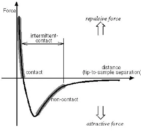
Figure 2.3 shows the relationship curves of force vs. distance between SPM tip and sample surface. It was observed that a force is attractive force when the SPM tip-to-sample surface distance was provided with a few micrometers. However, when the SPM tip-to-sample surface distance decreased to small that the force becomes repulsive force, and variated very violently with decreasing very small distance. In the contact regime, the cantilever is held less than a few angstroms from the sample surface, and the interatomic force between the cantilever and the sample is repulsive. In the non-contact regime, the cantilever is held on the order of tens to hundreds of angstroms from the sample surface, and the interatomic force between the cantilever and sample is attractive (largely a result of
Laser
PSPD
Detector
Sample Surface
Cantilever
Mirror
SPM Tip
Feedback
Circuits
System
PZT Scanner
(Piezoelectronic Scanner)
the long-range Vander Waals interactions). Both contact and non-contact imaging techniques are described in detail in the following sections.
Contact Mode:
In contact-AFM mode, also known as repulsive mode, an AFM-tip makes soft “physical contact” with the sample surface. The AFM-tip is attached to the end of a cantilever with a low spring constant, lower than the effective spring constant holding the atoms of the sample together. As the scanner gently traces the tip across the sample (or the sample under the AFM-tip), the contact force causes the cantilever to bend to accommodate changes in topography.
Figure 2.3 The relationship curves of interatomic force vs. distance between SPM tip and sample surface.
At the right side of the curve the atoms are separated by a large distance. As the atoms are gradually brought together, they first weakly attract each other. This attraction increases until the atoms are so close together that their electron clouds begin to repel each other
electro-statically. This electro-static repulsion progressively weakens the attractive force as the interatomic separation continues to decrease. The force goes to zero when the distance between the atoms reaches a couple of angstroms, about the length of a chemical bond. When the total Vander Waals force becomes positive (repulsive), the atoms are in contact. A capillary force exerted by the thin water layer often present in an ambient environment, and the force exerted by the cantilever itself. The capillary force arises when water wicks its way around the tip, applying a strong attractive force (about 10-8 N) that holds the tip in contact with the surface. Typically, the interatomic force operating range from 10-6 N to 10-8 N. Contact AFM can record topographic, frictional and elasticity variations with close to atomic resolution, allowing surface measurements and images on a scale beyond the capabilities of conventional microscopes.
Non-Contact Mode:
Non-contact mode AFM (NC-AFM) is one of several vibrating cantilever techniques in which an AFM cantilever is vibrated near the surface of a sample. The spacing between the tip and the sample for NC-AFM is on the order of tens to hundreds of angstroms as shown in Figure 2.3. NC-AFM is desirable because it provides a means for measuring sample topography with little or no contact between the tip and the sample surface. Like contact AFM, non-contact AFM can be used to measure the topography of insulators and semiconductors as well as electrical conductors.
The total force between the tip and the sample in the non-contact regime is very low, generally about 10-12 N. This low force is advantageous for studying soft or elastic samples. A further advantage is that samples like silicon wafers are not contaminated through contact with the tip. Because the force between the tip and the sample in the non-contact regime is low, it is more difficult to measure than the force in the contact regime, which can be several orders of magnitude greater. The small force values in the non-contact regime and the greater stiffness of the cantilevers used for NC-AFM are both factors that make the NC-AFM signal small, and therefore difficult to measure. Thus, in non-contact mode, the system vibrates a stiff cantilever near its resonant frequency (typically from 100 to 400 KHz) with the amplitude of a few tens of angstroms. NC-AFM does not suffer from the tip or sample degradation effects that are sometimes observed after taking numerous
scans with contact AFM. So, the NC-AFM is also preferable to contact AFM for measuring soft samples.
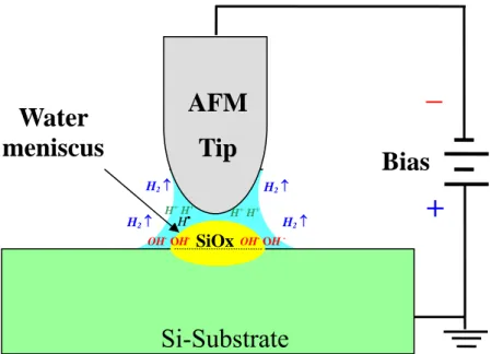
2.3 The mechanism of SPL field-induced local oxidation
Since the AFM-baesd field induce oxidation is performed under ambient conditions, a water bridge layer is always present on the sample surface. Sample surface passivation by surface hydrogenation impedes oxidation during the sample exposure to ambient air.As the hydrogen passivation layer can be locally removed by the additional electric field between the tip and the surface. And, the AFM-tip is biased negatively with respect to the sample surface; the sample surface starts to be oxidized when the addition bias exceeded a threshold voltage. The high growth rates occur at extreme electric field strengths near the apex of the AFM-tip of up to ~108 V/m. Field enhanced thin film oxidation can be modeled by Cabrera and Mott [12].
Figure 2.4 Distribution diagram of electric field exists between the apex of AFM-tip and the substrate surface.
The electric-field within the AFM-tip area can be calculated, assuming that the AFM-tip is considered as a charged sphere above can infinite conducting plane as is done
b
a
AFM Tip
R
V
Bias
Sample surface
for a STM tip. Figure 2.4 shows that the distribution diagram of electric field exists between the apex of AFM-tip and the substrate surface. The value of the electric field on the substrate surface located at a distance R from the projection on the sample of the apex of the AFM tip, can be expressed as follows [13]:
V
R
b
a
b
b
a
b
a
a
R
E
2 2 3/2]
)
[(
2
)
2
)(
(
)
(
+
+
+
+
=
………..……… (2.1)Where a is the sphere radius (about 10~15 nm), b is the AFM tip-sample surface distances, the electric field is strongly dependent on the AFM-tip-sample distance b.
The scanning probe lithography technique is realized by an electro-chemical reaction between the apex of the AFM-tip and the substrate surface, as shown in the Figure 2.5. Two chemical reactions are responsible for oxide formation during scanning probe lithography. Below the breakdown, electrons migrate from the Fermi level of the electrically biased AFM-tip into the water meniscus thus electrochemically reducing the water at the tip-surface interface and yielding hydroxyl ions (OH ) and (− H ) radicals as •
follows [14]: − • −
→
+
+
e
H
OH
O
H
2………..……..………… (2.2)
The hydroxyl ions ( −
OH ) are electro-statically attracted to the silicon surface, and
produce a silicon-oxide-like (SiO ) pattern. The (x
•
H ) radicals may recombine rapidly and
form the gas of molecular hydrogen ( H2 ) escaping from the reaction area. The
electrochemical reaction near the AFM-tip may be presented as follows:
− −
→
↑
+
+
e
H
OH
O
H
2
2
2
2 2…………..…………..…… (2.3)
Thus, an electric current during this reaction has a Faradiac character with conduction provided mainly by the migration of hydroxyl ions. The reaction at the silicon surface can be written as follows: + − −
−
→
+
+
OH
e
SiO
H
Si
2
4
22
…………..……… (2.4)So, the net electro-chemical reaction of scanning probe lithography resulting in silicon oxidation as follows:
![Figure 2.1 Principle of operation of the scanning tunneling microscope from the original article on the STM [3]](https://thumb-ap.123doks.com/thumbv2/9libinfo/8741069.204222/33.892.225.733.409.786/figure-principle-operation-scanning-tunneling-microscope-original-article.webp)