solution of the time-domain PMCHWT equations. Figure 8(a) shows the backscatter RCS from zero to 350 MHz by using different temporal basis functions. A good agreement with the Mie series solution is observed throughout the entire bandwidth using quadratic B-spline functions. The accuracy of the results using different temporal basis functions is compared in Figure 8(b), which shows that quadratic B-spline functions outperform both the second- and third-order Lagrange interpolating functions as tem-poral basis functions.
4. CONCLUSIONS
A numerical scheme that employs quadratic B-spline functions as temporal basis functions was described for solving TDIE of elec-tromagnetic scattering. Because these new temporal basis func-tions have a compact support and are complete to the second order, the resulting TDIE solution was shown to be more efficient and accurate than the commonly used Lagrange interpolating functions of the same order.
ACKNOWLEDGMENT
The first author thank Dr. Pei-lin Jiang and Dr. Zheng Lou for valuable discussions on time-domain integral equations.
REFERENCES
1. B. Shanker, A.A. Ergin, M. Lu, and E. Michielssen, Fast analysis of transient electromagnetic scattering phenomena using the multilevel plane wave time domain algorithm, IEEE Trans Antennas Propag 51 (2003), 628 – 641.
2. A.E. Yilmaz, J.M. Jin, and E. Michielssen, Time domain adaptive integral method for surface integral equations, IEEE Trans Antennas Propag 52 (2004), 2692–2708.
3. A.E. Yilmaz, J.M. Jin, and E. Michielssen, A parallel FFT accelerated transient filed-circuit simulator, IEEE Trans Microwave Theory Tech 53 (2005), 2851–2864.
4. G. Manara, A. Monorchio, and R. Reggiannini, A space-time discreti-zation criterion for a stable time-marching solution of the electric field integral equation, IEEE Trans Antennas Propag 45 (1997), 527–532. 5. P.L. Jiang and E. Michielssen, Temporal acceleration of time-domain integral equation solvers for electromagnetic scattering from objects residing in lossy media, Microwave Opt Technol Lett 44 (2005), 223–230.
6. Y.S. Chung, T.K. Sarkar, B.H. Jung, M. Salazar-Palma, Z. Ji, S. Jang, and K. Kim, Solution of time domain electric field integral equation using the Laguerre polynomials, IEEE Trans Antennas Propag 52 (2004), 2319 –2328.
7. Z. Ji, T.K. Sarkar, B.H. Jung, M. Salazar-Palma, and M. Yuan, A comparison of marching-on-in-time method with marching-on-in-de-gree method for the TD-EFIE solver, In: the proceedings of interna-tional conference on wireless communication and application in com-putational electromagnetics, 2005, pp. 297–300.
8. D.S. Weile, G. Pisharody, N.-W. Chen, B. Shanker, and E. Michiels-sen, A novel scheme for the solution of the time-domain integral equations of electromagnetics, IEEE Trans Antennas Propag 52 (2004), 283–295.
9. M.Y. Xia, G.H. Zhang, P. Wang, and C.H. Chan, Time domain integral equation method for transient analysis of wires using quadratic B-spline as temporal basis functions, IEEE Trans Antennas Propag, under review.
10. G. Pisharody and D.S. Weile, Electromagnetic scattering from homo-geneous dielectric bodies using time-domain integral equations, IEEE Trans Antennas Propag 54 (2006), 687– 697.
11. S.M. Rao, D.R. Wilton, and A.W. Glisson, Electromagnetic scattering by surfaces of arbitrary shape, IEEE Trans Antennas Propag 30 (1982), 409 – 418.
© 2007 Wiley Periodicals, Inc.
A LOW PHASE NOISE DESIGN FOR
ULTRAWIDEBAND FREQUENCY
SYNTHESIZER
Po-Yang Chang, Hui-I Wu, and Christina F. Jou Institute of Communication Engineering, National Chiao Tung University, Hsinchu, Taiwan
Received 24 September 2006
ABSTRACT: A low phase-noise frequency synthesizer design for
ultra-wideband is demonstrated in a 0.18-m CMOS process. It combines a low phase-noise voltage-controlled oscillator with two-stage dividers and a switched buffer multiplexer with low layout complexity. Because of the symmetrical independent architecture of this switch buffer design, it can reduce the additional phase noise created by the traditional multi-plexer stage. Here, this low phase noise design in three LO bands (8448, 4224, and 2112 MHz) is demonstrated. The measurement shows that in these three LO band, this new structure can achieve phase noise of less than⫺121 dBc/Hz at 1 MHz offset. The frequency tuning range is 10% while consuming only 52.2 mW from a 1.8-V supply. © 2007
Wiley Periodicals, Inc. Microwave Opt Technol Lett 49: 1159 –1162, 2007; Published online in Wiley InterScience (www.interscience.wiley. com). DOI 10.1002/mop.22384
Key words: frequency synthesizer; low phase noise; ultrawideband
1. INTRODUCTION
Ultrawideband (UWB) communication techniques have attracted great interests in both academia and industry in the past few years for applications in short-range and high-speed wireless mobile systems. As part of IEEE 802.15.3a, the spectrum is partitioned from 3 to 10 GHz into 528-MHz per bands and employs Orthog-onal Frequency Division Multiplexing in each band to transmit data rates as high as 480 Mb/s.
The frequency synthesizers used in UWB systems are usually designed with high frequency voltage-controlled oscillator (VCO), multistage dividers, and mixers so as to produce multiband LO signals [1, 2]. Since the UWB frequency synthesizer is a multiband structure with quadrature output, there are undoubtedly many signal transmission lines that cause more complexity of layout, thus affecting the phase noise of the synthesizer. Furthermore, the multiple differential pair structure is usually used in the conven-tional switched buffer multiplexer. The complexity of the multi-plexer layout often induces too much cross coupling effect. There-fore, in this article, we present a two-symmetrical independent architecture for the switched buffer multiplexer to reduce the phase noise in the multiband frequency synthesizer (see Fig. 4, one side of the switched buffer architecture).
The circuit architecture of this proposed low-phase noise UWB frequency synthesizer is shown in Figure 1, which is consisted of a binary CMOS VCO, two-stage frequency dividers, and a switched buffer with symmetrical independent architecture to crease the complexity in the multiplexer stage. The VCO is de-signed to have low phase noise performance by adding the tail capacitor to control the tail current (see Fig. 2). The whole archi-tecture is demonstrated in three selective LO bands (8448, 4224, and 2112 MHz) in fabrication of 0.18-m CMOS technology. This circuit achieves a measured phase noise of less than⫺121 dBc/Hz at 1 MHz offset and the frequency tuning range of 10% while consuming 52.2 mW from a 1.8-V supply.
2. BUILDING BLOCKS
2.1 Voltage-Controlled Oscillator
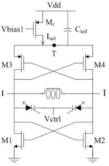
The VCO core design based on a cross-coupled negative-Gm topology is shown in Figure 2. It contains a negative-resistance LC-Resonator with cross-coupled pairs of FET transistors as active part. The architecture of the cross-coupled pairs adopts both NMOS (M1, M2) and PMOS (M3, M4) transistors to enhance
negative conductance. Here, the resonant tank consists of a 1.89 nH integrated spiral inductors and two MOS junction varactors.
For low phase noise consideration, the use of a PMOS tail-current source, Mt, is justified since the PMOS transistors have lower 1/f noise than NMOS [3]. In addition, the width of the tail transistor Mtmust be increased to further reduce the flicker noise, which thus lowers significantly the close-in phase noise of the VCO. The voltage swing across the resonator is proportional to tail-current Itailand the tank equivalent resistance; therefore, the tail-current, Itail, is optimized by the choice of Vbias1 value not only to obtain a sufficient drain current (for a large transconduc-tance) but also to ensure VCO’s startup while still maintaining low thermal noise and diminished the power consumption. A tail capacitor Ctail is used to attenuate both the high-frequency noise components of the tail current and the voltage variations on the tail node T. This results in more symmetric waveforms and smaller harmonic distortion in VCO outputs. This behavior is consistent with an improvement of the phase noise performances of the VCO [4].
2.2 Frequency Dividers
The internal dividing function is based on a master-slave D-type flip-flop. The clock inputs are driven by the VCO outputs, which typically have large amplitude to lower the phase noise. Figure 3 shows the divider core which contains the master-slave flip-flop. Vbias2 of the first divider is 0.9 V, and the maximum output amplitude can be increased by operating Mb1and Mb2in the linear region. Polysilicon resistors (RL) are chosen to have the same low resistance to lower the RC time constant for output nodes (Q3 and Q4). The transistor sizes were chosen such that the dc level and small-signal swing at the output of each stage can directly drive the Figure 1 Circuit architecture
Figure 2 Voltage controlled oscillator structure
Figure 3 Circuit schematic of the D Flip-flop
Figure 4 Controlled switched buffer used to change the carrier fre-quency
subsequent stage without fully restoring the signal level. This further reduces the power consumption and lowers the switching noise.
2.3 Switched Buffer
The simple structure of the multiplexer stage can lower the com-plexity of layout. Figure 4 consists of multiple cascode structures that share a common load R1. The signals to be selected are applied to the buffer, and MOS switches (S1–S3) activate one selected
band. The cascode structure is used to improve the reverse isola-tion; otherwise, the signal leakage will create a small unwanted tone at the LO outputs. The bias voltages are all 0.9 V to prevent the compression of the voltage swing and the capacitive effect. Rb
is chosen to be a large value to avoid signal loss.
The inverter is used in the buffer that supplies the transition between charge and discharge. A large resistor R2 connects the input and output to keep the output DC voltage to 0.9 V. Further-more, the reverse current from Vdd to 0.9 V bias can also be decreased effectively.
3. EXPERIMENTAL RESULTS
The synthesizer is fabricated in a 0.18-m CMOS process. The chip consumes an area of 0.9⫻ 1.1 mm2, as shown in Figure 5.
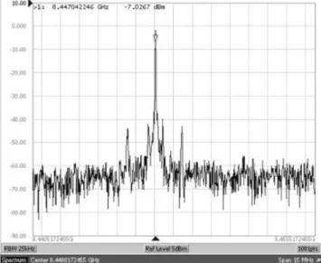
The circuit has been tested on a chip-on-board assembly. The measured core circuit consumes 31.92 mW and the buffer con-sumes 20.28 mW from a 1.8-V supply. Figure 6 shows the mea-sured tuning characteristics of the three bands, and the tuning ranges are 833, 401, and 203 MHz, respectively. Figure 7 shows the measured the spectrum of 8448 MHz in this frequency syn-thesizer. The measured phase noise of 8448 MHz is 121 dBc/Hz at 1-MHz offset by using the Agilent E5052A and E5053A Signal Source Analyzer (see Fig. 8). Table I summarizes the measured performance of this work.
4. CONCLUSION
In this article, a low phase-noise frequency synthesizer architecture design for UWB is demonstrated. The circuit is measured at 8448, 4224, and 2112 MHz in a standard TSMC 0.18-m CMOS 1P6M technology. By the low phase-noise VCO design and simplifying Figure 5 Chip micrograph
Figure 6 Tuning ranges of the three bands
Figure 7 Output spectrum of 8448 MHz (Span 15 MHz)
Figure 8 Phase noise of 8448 MHz
the switched buffer multiplexer, this work achieves the phase noise of less than ⫺121 dBc/Hz at 1 MHz offset and the frequency tuning range of 10% while consuming 52.2 mW from a 1.8-V supply.
ACKNOWLEDGMENT
The authors thank the Chip Implementation Center of the National Science Council, Taiwan, Republic of China, for supporting the TSMC CMOS process. This work was supported by Research Projects of the National Science Council, Taiwan, Republic of China, under Projects NSC 94 –2213-E-009 – 051, and the National Chip Implementation Center.
REFERENCES
1. A. Ismail and A.A. Abidi, A 3.1- to 8.2-GHz zero-IF receiver and direct frequency synthesizer in 0.18-/spl mu/m SiGe BiCMOS for mode-2 MB-OFDM UWB communication, IEEE J Solid-State Circuits 40 (2005), 2573–2582.
2. J. Lee, A 3-to-8-GHz fast-hopping frequency synthesizer in 0.18-/spl mu/m CMOS technology, IEEE J. Solid-State Circuits, 41 (2006), 566 –573.
3. K.O. Kenneth, N. Park, and D.J. Yang, 1/f noise of nMOS and pMOS transistors anf their implications to design of voltage controlled oscil-lators, IEEE Radio Frequency Integrated Circuit Symp Dig, Seattle, WA (2002), 59 – 62.
4. A. Hajimiri and T.H. Lee, Design issues in CMOS differential LC oscillators, IEEE J Solid-State Circuits 34 (1999), 717–724.
© 2007 Wiley Periodicals, Inc.
GAIN ENHANCEMENT OF A
DIELECTRIC RESONATOR ANTENNA
WITH USE OF SURFACE MOUNTED
SHORT HORN
Nasimuddin1,2and Karu P. Esselle2 1Institute for Infocomm Research, Singapore,
2Department of Electronics, Macquarie University, Sydney, Australia
Received 28 September 2006
ABSTRACT: We demonstrate the gain of a standard rectangular
di-electric resonator antenna (DRA) enhanced by integrating it with a sur-face mounted short horn (SMSH). An enhancement of gain by 3.8 dB to 8.5 dBi at 5.95 GHz, and a 10 dB return bandwidth of 3.2% has been achieved from this configuration. Total height of the fabricated structure is only 0.1720, or 8.61 mm at 6.0 GHz, and the aperture size is 0.960
⫻ 0.860,or 48.1 mm⫻ 43.1 mm. The cross-polarization level of the
an-tenna is⬍33 dB in both E- and H-planes. © 2007 Wiley Periodicals, Inc.
Microwave Opt Technol Lett 49: 1162–1166, 2007; Published online in Wiley InterScience (www.interscience.wiley.com). DOI 10.1002/mop. 22379
Key words: dielectric resonator antennas; high-gain; short horn; gain
enhancement
1. INTRODUCTION
Modern broadband communication systems and radars require lightweight compact antennas with high gain and wide bandwidth. Dielectric resonator antennas (DRAs) offer several advantages such as wide bandwidth, small size, ease of fabrication, and high radiation efficiency. A rectangular DRA can be designed as a compact, low profile antenna [1–3], but it suffers from low gain. Several efforts have been made to increase the gain of DRAs. They include employing an offset dual-disk dielectric resonator (DR) [4], stacking parasitic DRs with an air gap between a radi-ating patch and parasitic DRs [5], and using composite layered DRs of high permittivity [6]. These efforts resulted in a gain improvement of up to 2.7 dB over a single DRA element. Hakkak and Ameri [7] have achieved a 7 dBi gain from a dielectric TABLE 1 Summary of Measurement
Switch Mode S1 S2 S3 Frequency (MHz) 8448 4224 2112 Tuning range (MHz) 7648–8481 (10.3%) 3834–4235 (9.9%) 1914–2117 (10.1%) Phase noise (dBc/Hz) ⫺95.5 dBc at 100 KHz ⫺101.5 dBc at 100 KHz ⫺104.1 dBc at 100 KHz ⫺121.1 dBc at 1 MHz ⫺123.0 dBc at 1 MHz ⫺126.2 dBc at 1 MHz Output power (dBm) ⫺7.02 ⫺8.75 ⫺7.32 Total power 52.2 mW
Figure 1 (a) Antenna configuration. (b) Fabricated DRA with SMSH made from copper block