Resonant spin dipole induced by an in-plane potential gradient spin-orbit interaction
K. Y. Chen,1C. S. Chu,1and A. G. Mal’shukov1,2,3
1Department of Electrophysics, National Chiao Tung University, Hsinchu 30010, Taiwan 2Institute of Spectroscopy, Russian Academy of Science, 142190 Troitsk, Moscow oblast, Russia
3National Center for Theoretical Sciences, Hsinchu 30043, Taiwan 共Received 30 May 2007; published 11 October 2007兲
Spin-orbit interaction共SOI兲 arising from in-plane potential gradient is invoked for the generation of spin accumulation in a driven electric field. The SOI and a local in-plane potential pattern together bring about resonant spin dependent scatterings to electrons in a nonequilibrium distribution. In the vicinity of a ring-shaped potential barrier pattern, a spin dipole distribution with a resonant dipole strength characteristic is obtained. As the chemical potential is increased across one such resonant energy, the dipole strength manifests both sign reversal and large amplitude enhancement. The scattering resonance, thus, provides an additional knob for the manipulation of the spin accumulation.
DOI:10.1103/PhysRevB.76.153304 PACS number共s兲: 73.40.Lq, 72.25.Dc, 71.70.Ej
Spintronics exploits electron spin as the key physical en-tity for a new paradigm upon which novel device concepts and applications can be contrived.1,2 The recent intensive
studies on spin-Hall effect, where an external electric field leads to spin flow in the transverse direction, spin accumu-lation at lateral edges, and spin polarization in the bulk,3–14 demonstrate great interest in nonmagnetic generation of spin transport and accumulation in semiconductors.
The spin-orbit coupling is much larger in semiconduc-tors than in vacuum by a factor of, typically, 6 orders of magnitude. This factor is the ratio of the Dirac gap 共m0c2
= 0.5 MeV兲 in vacuum and an effective Dirac gap 共Eg
⬃1 eV兲 in semiconductor.15,16Various spin-orbit interactions
共SOIs兲 have been considered. Of intrinsic nature are the Rashba4,7,9–13 and Dresselhaus SOIs,6,11and of extrinsic
na-ture is the impurity-induced SOI.3,5,8,10,13 The Rashba SOI
originates from a structure inversion asymmetry—the asym-metry in the confinement potential normal to a quantum well 共QW兲. The Dresselhaus SOI originates from the inversion asymmetry in the crystal potential. The impurity-induced SOI is the atomiclike SOI albeit occurring in a semiconduc-tor host. We point out that the SOI due to in-plane potential gradient has largely been neglected even though there have been studies on scattering by microstructures in SOI two-dimensional electron gas 共2DEG兲.17–21 An exception is a
study on a smooth lateral potential.17 It is then of interest to
invoke the in-plane potential gradient SOI, to propose a rel-evant local in-plane potential pattern, and to study their reso-nant interplay. Very recently, strong in-plane gradient of the crystal potential in the surface layer of Bi/ Ag共111兲 alloy is identified as the major physics behind a giant spin splitting.22
Thus, the physics we explore here could also be of relevance to surface spintronics in metallic alloys.
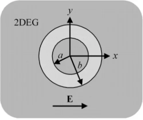
Of our major concern here is the in-plane potential gradi-ent SOI from a ring-shaped potgradi-ential barrier 共RSPB兲 in a symmetric QW, as shown in Fig.1. The Rashba SOI is neg-ligible in a symmetric QW, and the impurity-induced SOI effect turns out to be small. Expecting the physical picture to remain intact with the negligence of the Dresselhaus SOI, we leave the inclusion of it to future investigation. Driven by an electric field, electrons in a nonequilibrium distribution are
scattered by the RSPB. The scattering is spin dependent and asymmetric with respect to the scattering angle. It leads to a simultaneous pileup of charge and spin dipoles, within the ballistic range of the ring, which orient oppositely and trans-versely to the electric field, respectively. The charge dipole is the Landauer residual resistivity dipole.23,24 In a different
system, a spin dipole has also been found near the vicinity of a non-SOI scatterer in a Rashba SOI host.25,26 Our main
re-sult is that in-plane potential gradient SOI combined with transmission of a ring structure gives rise to a spin dipole of sufficiently large strength. As the Fermi energy is tuned across a resonant value, the spin dipole strength exhibits both large amplitude enhancement and sign reversal.
The RSPB V共兲 contributes to the SOI through a term of the form −共/ប兲1dVd共兲 L ·, where ⬇P32
关
E1g 2−
1 共Eg+⌬0兲2
兴
= 120 Å2for InAs,15,16,27L andare the orbital and the spinoperator, and⌬0 and P are, respectively, the energy of the split-off hole and the momentum matrix element between s and p orbitals. L ·= Lzz in a thin semiconductor film or a
QW. Thus, for a plane wave k= eik·r incident in the x
direction, wherez=and= ± 1, the spin does not flip
but the scattering is spin dependent. Cylindrical symmetry requires the total wave function in the form
FIG. 1. System configuration: A ring-shaped potential pattern in a two-dimensional electron gas 共2DEG兲, with radii a and b. An electric field E sets up a current in the 2DEG.
PHYSICAL REVIEW B 76, 153304共2007兲
⌿k共兲 =
兺
l=−⬁ l=+⬁ ilRl共兲e il共−k兲 , 共1兲where l, , and k are the azimuthal angular momentum
quantum number and angles of and k with xˆ, respectively.
Rl共兲 satisfies the equation
1 d d d dRl +
冋
k2−2m * ប2冉
V − dV dl冊
− l2 2册
Rl= 0, 共2兲 with the particle energy E =ប2k2/ 2m*. For a ring-shaped bar-rier, V共兲=V0关共− a兲−共− b兲兴, with a and b the inner and the outer radius, respectively, the radial function Rl共兲 has the form Rl共兲 =冦
ClJl共k兲, ⬍ a Al关Jl共兲 − BlYl共兲兴, a⬍⬍ b ei␦l关cos␦ l J l共k兲 − sin␦lYl共k兲兴, b ⬍,冧
共3兲 where Jl共k兲 and Yl共k兲 are Bessel functions of the first andthe second kind, respectively,=
冑
k2− 2m*V0/ប2is the wave vector in the barrier region, and␦l is the phase shift, which
we obtain to be ␦l= tan−1
冋
kbJl⬘
共kb兲 −␥l2Jl共kb兲 kbYl⬘
共kb兲 −␥l2Yl共kb兲册
. 共4兲 Here, ␥li=关
dln Rl d兴
=di−0+⫿ 2m*lV 0 ប2 , where i = 1 共2兲 denotesdi= a 共b兲 and upper 共lower兲 sign, Bl=
关
Jl⬘
共a兲−␥l1
aJl共a兲
兴
/关
Yl⬘
共a兲−␥l1
aYl共a兲
兴
, and Jl⬘
共x兲=dJl共x兲/dx.Tak-ing the limit a = b, one would get␦l= 0, as it should.
Resonant energies are obtained from the energy depen-dence of the phase shift, at which ␦l deviates from its
smooth general trend and exhibits abrupt change across a value of␦l=/ 2. More than one resonant characteristics can
be found in␦lfor a given l. These are associated with radial quantum number n. The excellent alignment of low lying resonant energies with the bound state energies of a cylindri-cal hard wall of radius a corroborates the role of quantum number n in the␦lresonances. S-wave共l=0兲 resonances in
␦l, however, will not show up in the spin dipole resonance
for the zero value of the SOI.
Driven by E = E0xˆ, the nonequilibrium electron
distribu-tion g共k兲=−eប
m*E · k␦共k−兲, where e⬎0 and and are,
respectively, the momentum relaxation time and the chemical potential. The spin density, with spin in units ofប/2, is given by Sz共兲 = 1 42
冕
dkg共k兲兺
⌿k † 共兲⌿ k共兲, 共5兲which can be simplified to
Sz共兲 = nERe
兺
兺
l=0⬁
Rl共兲Rl+1*共兲sin 共6兲
by the use of the relation Rl=共−1兲lR
−l
−. The factor n
E
=eE0k
ប depends linearly on E0, and k is the Fermi wave vec-tor corresponding to the Fermi energy. The angular depen-dence, sin, of the spin density Sz共兲 in Eq. 共6兲 indicates a
dipole distribution: aligned both in-plane and normal to E. The spin density expression holds within a mean free path distance from the ring.
Presentation of our result is facilitated by a spin dipole strength ps defined from the asymptotic behavior共kFⰇ1兲.
Averaging out the Friedel oscillations, the asymptotic expres-sion of Szand its lowest correction term is given by
Sz= sin k*
冋
ps+ 㜷s k*册
, 共7兲 where ps= − nE*k⬜ 4 . 共8兲The constant factor nE* represents a typical value of nEin
Eq.共6兲, with Fermi wave vector k replaced by a typical value
k*. Casting into the form nE
* =m *eE 0l0* ប2 , with l0 * =បk*/ m*, its meaning is clearly shown to be the product of the two-dimensional density of states, m*/共ប2兲, and the work done
eE0l0* by the electric field within l0*. Specific value of k* de-pends on the system of our interest, and will be chosen in the following numerical example. The factor k⬜is essentially a transverse moment of the spin dependent part of the differential cross section D共兲, given by ⬜ =兰02dsin兺⬘
⬘
D⬘共兲, where D共兲=2k1 兩兺l=0⬁ 共e2i␦l− 1兲eil兩2. In terms of the phase shifts, ⬜= 2 k
兺
兺
l=0 ⬁ sin关2共␦l−␦l+1 兲兴, 共9兲 㜷s= 1 4nE*k*⬜⬘
and ⬜⬘
= 1 k⌺⌺l=0⬁ 共2l+1兲cos关2共␦l−␦l+1 兲兴.Our key results are in Eqs.共6兲–共9兲.
In Fig.2, we present thedependence of k⬜. Parameter units typical for InAs are electron density ne
* = 7.4 ⫻1011cm−2, energy unit E*= n
e
*ប2/ m*= 77.1 meV, m* = 0.023me, k*= 2.16⫻108m−1, and length unit L*= 1 / k*
= 46.3 Å. In these units, the ring-shaped potential has radii
a = 14 and b = 20.5, barrier potential V0= 0.75, mean free path
l0*= 238, and E0= 0.1 kV/ cm. The spin dipole strength ps is
fully characterized by k⬜ except for a factor nE
*
/ 4= 8.4 ⫻109cm−2. As shown in Fig.2共a兲, k
⬜contains many reso-nant structures: each resonance is represented by a pair of peak and dip spikes. The resonant enhancement is large: away from resonances, 兩k⬜兩⬇10−1, but at resonance, its maximum magnitude can reach up to 7 such that the en-hancement factor reaches 70. The resonant profile invites grouping into different series, each associated with a radial quantum number n. The first 共n=1兲 series starts from = 0.064, consisting of the largest resonant amplitudes, and with l starting from l = 1 and onward until over 16. The n
BRIEF REPORTS PHYSICAL REVIEW B 76, 153304共2007兲
= 2 and n = 3 series start from= 0.213 and= 0.44, respec-tively. The low lying resonant energies共Ⰶ0.75兲 align very well with the bound state energies in a cylindrical hard wall of radius a. Higher resonant energies are slightly redshifted relative to the bound state energies, while the resonant widths are widened.
Further confirmation that each peak-dip resonant pair in
k⬜is due to a single resonance event is obtained by close inspection of the resonant pairs: the 共n=1, l=4,5,6兲 reso-nances in Figs.2共b兲 and2共c兲, respectively. The solid curves are full summations of k⬜according to Eq.共9兲; the dotted-dashed curves are partial summations of k⬜, including only terms that involve ␦l=5 ; and the dashed curves are the full summation of k⬜, but for V0= 0.751. The dotted-dashed curve matches very well with the共1,5兲 structure, but repro-duces only qualitative features for the共1,4兲 and 共1,6兲 struc-tures. Thus, the resonant pair at l = 5 is directly associated with the resonant behavior of the phase shift ␦l=5 . That the same partial summation also reproduces qualitative reso-nance features for l = 14 and l = 16 is because the partial sum-mation has included some but not all terms involving ␦l=4 and␦l=6 . The effect of increasing V0is shown to cause blue-shifted and sharper resonant structures, which, again, cor-roborate our scattering resonance picture.
The summation expression of k⬜in Eq.共9兲 is also useful in understanding the origin of the peak-dip pair at each reso-nance. Setting to zero, the summation 兺l=0⬁ sin关2共␦l
−␦l+1 兲兴 becomes spin independent, with peaks at the resonant energy Enl
0
. Recovering , the peak energy is shifted to Enl,
with the direction of energy shift opposite for opposite spin. It is the difference between these two shifted peaks that gives rise to the peak-dip pairs in k⬜. Interesting competition feature can also be observed in Fig.2共a兲. The peak-dip pairs in an n series trace out an envelope, the amplitude of which increases in low l and decreases at high l. This demonstrates the competition between the trend of stronger SOI for larger
l and the trend of weakening of the resonance due to wider
resonance width at higher energy.
In Fig.3, we present the radial variation of the spin den-sity Sz共兲. Energies at 0.3312 关Fig. 3共a兲兴 and 0.3328 关Fig.
3共b兲兴, are the peak and dip energies, respectively, of the l = 5 resonance in Fig.2. The dashed curves denote the first term in Eq.共7兲, and the dotted-dashed curves are the adjusted asymptotic behavior, including the㜷s term. Apart from the
Friedel oscillations, the dotted-dashed curves trace the asymptotic spin distribution remarkably. Figures 3共a兲 and 3共b兲show that the sign of the spin density can be reversed by a small change in ⌬= 0.0016E*, or 0.12 meV. The spin
FIG. 2. 共Color online兲 共a兲 k⬜ versus the Fermi energy, with energy unit E*= 77.1 meV. The radii of the RSPB are a = 14 and b = 20.5, respectively, and V0= 0.75. 共b兲–共d兲 Blowups of the n = 1, l = 4 , 5 , 6 resonances, respectively. The dotted-dashed 共purple兲 curves represent partial summations of k⬜, including only terms that in-volve␦l=5 . The dashed共blue兲 curves are the full summation for the case of V0= 0.751. The small-est abscissa division in共b兲–共d兲 is 0.0001.
FIG. 3. 共Color online兲 Radial dependence of Sz共兲 for =/2
and for /E*= 0.3312 共a兲 and 0.3328 共b兲, corresponding, respec-tively, to the peak and the dip of the l = 5 resonance in k⬜in Fig.
2. The dashed 共green兲 and dotted-dashed 共purple兲 curves are, re-spectively, the asymptotic behavior characterized by psand the
ad-justed asymptotic behavior when㜷sis also included. The vertical
dotted lines denote the ring region. At k*=50, S
z= −9.276m2共a兲
and 9.568m−2共b兲, respectively.
BRIEF REPORTS PHYSICAL REVIEW B 76, 153304共2007兲
density at k*= 50,= 0.23m, is共a兲 −9.276m−2 and共b兲 9.568m−2 or, in terms of the electron density n = 2.45 ⫻1011cm−2, the spin density is共a兲 0.379% and 共b兲 0.39%, respectively, of n, which is certainly large enough for observation.28The spin density at k*= 100 is one-half of the
above results. Finally, in Fig. 4, we present both the radial and the angular dependence of the spin dipole for the case of = 0.3312.
The proposed RSPB pattern is expected to be within reach by recent development in integrating focused ion beam and molecular beam epitaxy,29 where patterned ␦-doped layers
are fabricated. The steplike potential profile model offers a clear physical picture, and the results remain qualitatively intact if the potential profile is replaced by a smooth profile.30
In conclusion, we have shown that the in-plane potential gradient SOI and scattering resonance together can give rise to significant spin polarization. In our case here, it is in the form of a spin dipole, and the enhancement factor from reso-nance is large. Finally, the resoreso-nance provides us an impor-tant feature: an electrical way of switching the sign of the accumulated spin density by a simple control of the electron density.
The work was supported by the National Science Council of ROC under Grants No. NSC95-2112-M-009-004 and No. NSC93-2119-M-007-002 共NCTS兲, the RFBR Grant No. 060216699, and the MOE-ATU grant. The authors are grate-ful to the Center for Advanced Study in Oslo for hospitality. One of the authors共C.S.C.兲 acknowledges useful discussion with S. Q. Shen and the hospitality of the University of Hong Kong.
1Semiconductor Spintronics and Quantum Computation, edited by D. D. Awschalom, N. Samarth, and D. Loss共Springer-Verlag, Berlin, 2002兲.
2I. Zutic, J. Fabian, and S. Das Sarma, Rev. Mod. Phys. 76, 323 共2004兲.
3M. I. D’yakonov and V. I. Perel, JETP Lett. 13, 467共1971兲. 4V. M. Edelstein, Solid State Commun. 73, 233共1990兲. 5J. E. Hirsch, Phys. Rev. Lett. 83, 1834共1999兲.
6S. Murakami, N. Nagaosa, and S. C. Zhang, Science 301, 1348 共2003兲.
7J. Sinova, D. Culcer, Q. Niu, N. A. Sinitsyn, T. Jungwirth, and A. H. MacDonald, Phys. Rev. Lett. 92, 126603共2004兲.
8Y. K. Kato, R. C. Myers, A. C. Gossard, and D. D. Awschalom, Science 306, 1910共2004兲.
9J. Wunderlich, B. Kaestner, J. Sinova, and T. Jungwirth, Phys. Rev. Lett. 94, 047204共2005兲.
10H. A. Engel, B. I. Halperin, and E. I. Rashba, Phys. Rev. Lett. 95, 166605共2005兲.
11A. G. Mal’shukov, L. Y. Wang, C. S. Chu, and K. A. Chao, Phys. Rev. Lett. 95, 146601共2005兲.
12J. Sinova, S. Murakami, S. Q. Shen, and M. S. Choi, Solid State Commun. 138, 214共2006兲.
13W. K. Tse and S. DasSarma, Phys. Rev. B 74, 245309共2006兲. 14S. Q. Shen, Phys. Rev. Lett. 95, 187203共2005兲.
15E. I. Rashba, Physica E共Amsterdam兲 34, 31 共2006兲.
16R. Winkler, Spin-orbit Coupling Effects in Two-dimensional
Elec-tron and Hole System共Springer-Verlag, Berlin, 2003兲.
17A. O. Govorov, A. V. Kalameitsev, and J. P. Dulka, Phys. Rev. B
70, 245310共2004兲.
18H. Chen, J. J. Heremans, J. A. Peters, A. O. Govorov, N. Goel, S. J. Chung, and M. B. Santos, Appl. Phys. Lett. 86, 032113 共2005兲.
19J. D. Walls, J. Huang, R. M. Westervelt, and E. J. Heller, Phys. Rev. B 73, 035325共2006兲.
20J. Y. Yeh, M. C. Chang, and C. Y. Mou, Phys. Rev. B 73, 035313 共2006兲.
21A. Pályi, C. Péterfalvi, and J. Cserti, Phys. Rev. B 74, 073305 共2006兲.
22C. R. Ast, J. Henk, A. Ernst, L. Moreschini, M. C. Falub, D. Pacilé, P. Bruno, K. Kern, and M. Grioni, Phys. Rev. Lett. 98, 186807共2007兲.
23R. Landauer, IBM J. Res. Dev. 1, 223共1957兲; Philos. Mag. 21, 863共1970兲.
24R. S. Sorbello and C. S. Chu, IBM J. Res. Dev. 32, 58共1988兲; C. S. Chu and R. S. Sorbello, Phys. Rev. B 38, 7260共1988兲. 25A. G. Mal’shukov and C. S. Chu, Phys. Rev. Lett. 97, 076601
共2006兲.
26A. G. Mal’shukov, L. Y. Wang, and C. S. Chu, Phys. Rev. B 75, 085315共2007兲.
27P. Noziéres and C. Lewiner, J. Phys.共Paris兲 34, 901 共1973兲. 28V. Sih, W. H. Lau, R. C. Myers, V. R. Horowitz, A. C. Gossard,
and D. D. Awschalom, Phys. Rev. Lett. 97, 096605共2006兲. 29T. Hada, T. Goto, J. Yanagisawa, F. Wakaya, Y. Yuba, and K.
Gamo, J. Vac. Sci. Technol. B 18, 3158共2000兲.
30K. Y. Chen, C. S. Chu, and A. G. Mal’shukov共unpublished兲. FIG. 4. 共Color online兲 Spatial distribution of Sz共兲. Fermi
en-ergy/E*= 0.3312 for the Fig.3共a兲case, and E is along xˆ. The ring region is denoted both by the gray circular bar and by the concentric circles on the projected x = y plane.
BRIEF REPORTS PHYSICAL REVIEW B 76, 153304共2007兲