Trenched epitaxial lateral overgrowth of fast coalesced a -plane GaN with low
dislocation density
Te-Chung Wang, Tien-Chang Lu, Tsung-Shine Ko, Hao-Chung Kuo, Min Yu, Sing-Chung Wang, Chang-Cheng Chuo, Zheng-Hong Lee, and Hou-Guang Chen
Citation: Applied Physics Letters 89, 251109 (2006); doi: 10.1063/1.2405880 View online: http://dx.doi.org/10.1063/1.2405880
View Table of Contents: http://scitation.aip.org/content/aip/journal/apl/89/25?ver=pdfcov Published by the AIP Publishing
Articles you may be interested in
Nanorod epitaxial lateral overgrowth of a -plane GaN with low dislocation density Appl. Phys. Lett. 94, 251912 (2009); 10.1063/1.3158954
Epitaxial lateral overgrowth of a -plane GaN by metalorganic chemical vapor deposition J. Appl. Phys. 102, 053506 (2007); 10.1063/1.2773692
Defect reduction in ( 11 2 ¯ 0 ) a -plane GaN by two-stage epitaxial lateral overgrowth Appl. Phys. Lett. 89, 262105 (2006); 10.1063/1.2423328
Defect reduction in nonpolar a -plane GaN films using in situ Si N x nanomask Appl. Phys. Lett. 89, 041903 (2006); 10.1063/1.2234841
Correlation of strain, wing tilt, dislocation density, and photoluminescence in epitaxial lateral overgrown GaN on SiC substrates
J. Appl. Phys. 96, 3666 (2004); 10.1063/1.1784617
This article is copyrighted as indicated in the article. Reuse of AIP content is subject to the terms at: http://scitation.aip.org/termsconditions. Downloaded to IP: 140.113.38.11 On: Thu, 01 May 2014 01:40:59
Trenched epitaxial lateral overgrowth of fast coalesced a-plane GaN
with low dislocation density
Te-Chung Wang, Tien-Chang Lu,a兲,b兲 Tsung-Shine Ko, Hao-Chung Kuo,a兲,c兲 Min Yu, and Sing-Chung Wang
Department of Photonics and Institute of Electro-Optical Engineering, National Chiao Tung University, Hsinchu, Taiwan 300, ROC
Chang-Cheng Chuo and Zheng-Hong Lee
Electronics and Optoelectronics Research Laboratories, Industrial Technology Research Institute, Dashu Township, Kaohsiung County 840, Taiwan, ROC
Hou-Guang Chen
Department of Materials Science and Engineering, I-Shou University, Hsinchu, Taiwan 310, ROC
共Received 29 August 2006; accepted 9 November 2006; published online 19 December 2006兲 The crystal quality of a-plane GaN films was improved by using epitaxial lateral overgrowth on trenched a-plane GaN buffer layers. Not only the threading dislocation density but also the difference of anisotropic in-plane strain between orthogonal crystal axes can be mitigated by using trenched epitaxial lateral overgrowth共TELOG兲. The low threading dislocation density investigated by the cross-sectional transmission electron microscopy was estimated to be 3⫻107cm−2 on the
N-face GaN wing. On the other hand, the Ga-face GaN wing with a faster lateral overgrowth rate could be influenced by the thin GaN layer grown on the bottom of the trenches, resulting in higher dislocation density generated. As a result, the authors concluded that a narrower stripped GaN seeds and deeper stripped trenches etched into the surface of sapphire could derive a better quality a-plane GaN film. Finally, they demonstrated the fast coalescence process of TELOG GaN films below 10m thick. © 2006 American Institute of Physics. 关DOI:10.1063/1.2405880兴
The radiative quantum efficiency of nitride light emitters grown along关0001兴 c direction is low due to the presence of built-in electric fields, by the spontaneous and piezoelectric polarizations separating the electron and hole spatial distri-butions to incline the band structure and reduce oscillator strength in the quantum wells.1 Since the performances of III-nitride devices are limited by the polarization-related in-ternal electric fields, nonpolar GaN is currently the subject of intense research due to the potential to improve the internal quantum efficiency of GaN optoelectronic devices. To elimi-nate such polarization effects, growth along nonpolar orien-tations has been, respectively, explored for 关112¯0兴 a-plane GaN on 关101¯2兴 r-plane sapphire2 and a-plane SiC,3 and 关101¯0兴 m-plane GaN on 关100兴 LiAlO2 substrates.4,5
How-ever, nonpolar a-plane GaN based material grown on r-plane sapphire substrates always accompanies with a wavy, stripe-like growth feature and possess a large density of threading dislocations and stacking faults. In addition, the lattice mis-match between a-plane GaN and r-plane sapphire results in serious anisotropic in-plane strain difference between or-thogonal crystal axes.6Recently, successful epitaxial lateral overgrowth共ELOG兲 of a-plane GaN on r-plane sapphire has been reported,7 which significantly improves the material quality by reducing the density of threading dislocations and alleviates the strain-related surface roughening and faceting.7 Despite the ELOG assisted morphology and quality improve-ments in a-plane GaN over r-plane sapphire, the coalescence thickness, usually more than 20m, is quiet thick and diffi-cult to control the uniformity. In this letter, we improve
关112¯0兴 a-plane GaN quality by using epitaxial lateral over-growth on trenched a-plane GaN buffer layers. The trenched epitaxial lateral overgrowth共TELOG兲 allowed us to obtain
a-plane GaN with low dislocation density, simple fabrication
process, lower cost, and thinner coalescence thickness in comparisons to the previous reports.
Figure 1 shows the flow chart to grow the TELOG
a-GaN. First, the a-plane GaN templates with 1.5m thick-ness were grown by low pressure metal-organic chemical vapor deposition共MOCVD兲 on r-plane Al2O3 sapphire
sub-strates using conventional two-step growth technique. Then, a 2m seed/18m trench TELOG stripe pattern was ap-plied parallel to the 关11¯00兴 direction to realize vertical
c-plane sidewalls followed by etching of SiO2 using
induc-tively coupled plasma etching through the windows to the GaN epitaxial film. GaN stripes were etched through the mask openings, down to the r-plane sapphire substrate by
a兲Author to whom correspondence should be addressed. b兲Electronic mail: [email protected]
c兲Electronic mail: [email protected] FIG. 1. Flow chart of a-plane GaN TELOG process.
APPLIED PHYSICS LETTERS 89, 251109共2006兲
0003-6951/2006/89共25兲/251109/3/$23.00 89, 251109-1 © 2006 American Institute of Physics
This article is copyrighted as indicated in the article. Reuse of AIP content is subject to the terms at: http://scitation.aip.org/termsconditions. Downloaded to IP: 140.113.38.11 On: Thu, 01 May 2014 01:40:59
reactive ion etching. To simplify the growth process, the SiO2 mask was removed by hydrofluoric acid followed by depositing a-plane GaN TELOG film using a single-step growth process. In this study, the growth temperature, pres-sure, and V/III ratio were 1190 ° C, 100– 150 mbars, and 700–800, respectively. The grown samples were investigated by scanning electron microscopy 共SEM兲, high-resolution x-ray diffraction, and transmission electron microscopy 共TEM兲. We also used a scanning optical microscopy to scan a 25⫻25m2 microphotoluminescence 共-PL兲 mappings
with spatial and spectral resolutions of 1m and 1 nm, re-spectively, pumped by a He–Cd laser operating on 325 nm with 25 mW.
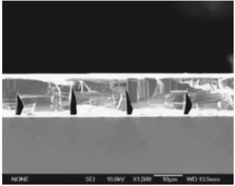
To observe the growth mechanism, we stopped the pro-cess before the coalescence of the GaN films. The SEM im-ages of cross-sectional and birds-view TELOG GaN by MOCVD were shown in Fig. 2共a兲. The growth rate of the Ga-face wing was twice faster than the N-face wing. How-ever, the ratio of growth rate in Ga-face wing to N-face wing was not as high as an order of magnitude reported by Imer
et al.8A thin GaN layer about 0.2m grown on the bottom of the trenches, as shown in Fig.2共b兲, could be the reason to hinder the lateral growth rate in the Ga-face wing and hence affect the epitaxial quality.
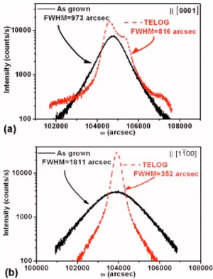
High-resolution x-ray rocking curves along关0001兴 c and 关11¯00兴 m directions were shown in Fig.3. The full width at half maximum共FWHM兲 of x-ray rocking curves for an as-grown a-GaN 1.5m bulk layer in 关11¯00兴 direction is al-most twice as large as that in关0001兴 direction. It shows that the strains between the orthogonal crystal axes, c-axis and
m-axis, are quite different and enhance the formation of line
defects. Moreover, the surface geometry could show a wavy, stripelike growth feature if the nucleation layer was not op-timized or the epitaxial film was thick.2However, after lat-eral overgrowth, the stresses of TELOG layer were released in both c axis and m axis and thus the crystal quality was enhanced especially in the关11¯00兴 direction. As shown in Fig.
3, the FWHM of x-ray rocking curves for a TELOG layer was reduced from 1811 to 352 arc sec. Since the strip of the
TELOG layer did not coalesce, we observed obvious wing tilt phenomenon along关0001兴 direction leading to the broad-ening effect of the x-ray rocking curve. Unlike the symmetric wing tilt in c-plane ELOG GaN,9,10 the wing tilt in a-plane TELOG GaN is asymmetric shown in the x-ray rocking curve, resulting from the different lateral growth rates of the window GaN in the关0001兴 and the 关0001¯兴 directions.7,11 Al-though the FWHM of x-ray rocking curves for a TELOG layer was only reduced from 973 to 816 arc sec, the crystal quality would be better as the TELOG film fully coalesced to lessen wing tilt phenomenon.
Figure 4共a兲shows a -PL mapping of a-plane TELOG stripes. As shown in Fig.4共a兲, five different regions can be distinguished in the TELOG sample and were labeled with numbers 1–5. Comparing the-PL mapping with the SEM image, region 5 showing the lowest-PL intensity area can be identified as the uncoalesced trenched region since
a-GaN grown on r sapphire without a nucleation layer
showed a textured surface with worst crystal quality. On the other hand, region 1 showing the strongest -PL intensity area can be identified as the N-face GaN wing. Region 2 is the stripped a-GaN seed. Regions 3 and 4 belong to the Ga-face GaN wing. Interestingly, region 3 standing at the initial region of the Ga-face GaN wing shows a higher PL intensity than that in region 4.
The distributions and types of dislocations were investi-gated by cross-sectional TEM shown in Figs.4共b兲and4共c兲. According to the g =共0002兲 and g=共112¯0兲 two beam bright field images, most of the threading dislocations are obvious in both of the g =共112¯0兲 and 共0002兲 two beam conditions, indicating that these dislocations are mixed a + c type dislo-cations. The distribution of dislocations in Figs.4共b兲and4共c兲 cab also be labeled with numbers 1–5 fully corresponding to the -PL mapping results. The threading dislocation densi-ties共TDDs兲 of stripped GaN seed in region 2 was more than 1⫻1010cm−2. TDD of Ga-face GaN wing in region 4 was
FIG. 2. Cross-sectional SEM of the uncoalesced TELOG a-plane GaN film with 2m seed/18m trench pattern.
FIG. 3. 共Color online兲 X-ray rocking curves of as-grown and TELOG
a-plane GaN films共a兲 along 关0001兴 direction 共b兲 along 关11¯00兴 direction.
251109-2 Wang et al. Appl. Phys. Lett. 89, 251109共2006兲
This article is copyrighted as indicated in the article. Reuse of AIP content is subject to the terms at: http://scitation.aip.org/termsconditions. Downloaded to IP: 140.113.38.11 On: Thu, 01 May 2014 01:40:59
about 9⫻109cm−2 and TDD of N-face GaN wing in region
1 was about 3⫻107cm−2, three orders of magnitude lower
than planar films. The lower dislocation density in region 3 in comparison to region 4 was in accordance with a higher PL intensity. Because the lateral growth mode could be af-fected when the laterally grown layers encounters the under-lying GaN layers, we suggest that the crystal quality of Ga-face GaN with a higher growth rate could be easily af-fected by the thin a-GaN layer grown on the bottom of the uncoalesced windows. Due to the relatively low growth rate of the thin a-GaN layer on the bottom of the trench, the crystal quality of the Ga-face GaN wing at the beginning of the lateral growth was good while the thin a-GaN layer was not formed, resulting in a low dislocation and high PL inten-sity area of region 3. According to the results of SEM image, the rough GaN layer grown on the window of TELOG with-out smooth nucleation layer is difficult to grow more than 0.2m. As a result, to obtain a better crystal quality a-plane TELOG GaN for the most of the area, the trench depth shall be down to at least 0.2m deeper than the sapphire surface to prevent the coalescing between the TELOG layer and thin GaN layer.
We then continue to perform the TELOG process with a 2m seed /18m trench stripe pattern to obtain a fully coalesced a-plane GaN film, as shown in the SEM image of Fig.5. The coalescence process can fully be completed for the thickness around 10m, it is a useful technique to over-come the thickness problem that the previous ELOG always needs more than 30m to fully coalesce.8 The FWHM of x-ray curves can be reduced to 385 arc sec in 关0001兴 and
260 arc sec in 关11¯00兴 directions without wing tilt phenom-enon demonstrating not only a high crystal quality but also an isotropic characteristic of a-plane TELOG GaN films.
In conclusion, we have grown high quality and fully coalesced a-plane GaN films at the thickness of 10m by using TELOG with a 2m seed/18m trench stripe pattern. The FWHMs of x-ray rocking curves along 关0001兴 c and 关11¯00兴 m directions were reduced from 973 to 385 arc sec and from 1811 to 260 arc sec, respectively, demonstrating the improvement of the crystal quality and the mitigation of the anisotropic in-plane strains between different crystal axes by TELOG. According to the results of-PL mapping and TEM, the TDD can be reduced largely from 1⫻1010 to 3
⫻107cm−2 for the N-face GaN wing. The Ga-face GaN
could be much easily influenced by the thin GaN layer grown on the bottom of trench, indicating that a narrower stripped GaN seeds and deeper trench etched into the surface of sapphire can derive a better quality a-plane TELOG GaN film for the most of the area.
The authors would like to specially acknowledge the fi-nancial support by the Ministry of Economic Affairs, Tai-wan, Republic of China, the MOE ATU program, and the National Science Council of Republic of China 共ROC兲 in Taiwan under Contract Nos. NSC 94-2120-M-009-007 and NSC 94-2215-E-009-082.
1P. Waltereit, O. Brandt, A. Trampert, H. T. Grahn, J. Menniger, M.
Ram-steiner, M. Reiche, and K. H. Ploog, Nature共London兲 406, 865 共2000兲.
2M. D. Craven, S. H. Lim, F. Wu, J. S. Speck, and S. P. DenBaars, Appl.
Phys. Lett. 81, 469共2002兲.
3M. D. Craven, A. Chakraborty, B. Imer, F. Wu, S. Keller, U. K. Mishra, J.
S. Speck, and S. P. DenBaars, Phys. Status Solidi C 1, 4共2003兲.
4E. S. Hellman, Z. Liliental-Weber, and D. N. E. Buchanan, MRS Internet
J. Nitride Semicond. Res. 2, 30共1997兲.
5P. Waltereit, O. Brandt, M. Ramsteiner, A. Trampert, H. T. Grahn, J.
Menniger, M. Reiche, R. Uecker, P. Reiche, and K. H. Ploog, Phys. Status Solidi A 180, 133共2000兲.
6H. Wang, C. Chen, Z. Gong, J. Zhang, M. Gaevski, M. Su, J. Yang, and M.
A. Khan, Appl. Phys. Lett. 84, 499共2004兲.
7M. D. Craven, S. H. Lim, F. Wu, J. S. Speck, and S. P. DenBaars, Appl.
Phys. Lett. 81, 1201共2002兲.
8B. M. Imer, F. Wu, S. P. DenBaars, and J. S. Speck, Appl. Phys. Lett. 88,
061908共2006兲.
9P. Fini, H. Marchand, J. P. Ibbetson, S. P. DenBaars, U. K. Mishra, and J.
S. Speck, J. Cryst. Growth 209, 581共2000兲.
10W. M. Chen, P. J. McNally, K. Jacobs, T. Tuomi, A. N. Danilewsky, Z. R.
Zytkiewicz, D. Lowney, J. Kanatharana, L. Knuuttila, and J. Riikonen, J. Cryst. Growth 243, 94共2002兲.
11C. Chen, J. Yang, H. Wang, J. Zhang, V. Adivarahan, M. Gaevski, E.
Kuokstis, Z. Gong, M. Su, and M. Asif Khan, Jpn. J. Appl. Phys., Part 2
42, L640共2003兲.
FIG. 4.共Color online兲 共a兲 Top view-PL image of TELOG a-plane GaN film.关共b兲 and 共c兲兴 Cross-sectional TEM g=共0002兲 and g=共112¯0兲 two beam bright field images.
FIG. 5. Cross-sectional SEM of fully coalesced TELOG a-plane GaN film with 2m seed/18m trench pattern.
251109-3 Wang et al. Appl. Phys. Lett. 89, 251109共2006兲
This article is copyrighted as indicated in the article. Reuse of AIP content is subject to the terms at: http://scitation.aip.org/termsconditions. Downloaded to IP: 140.113.38.11 On: Thu, 01 May 2014 01:40:59