行政院國家科學委員會專題研究計畫 成果報告
光學用自身組織塊式高分子/量子點奈米複合材料(3/3)
計畫類別: 整合型計畫 計畫編號: NSC94-2120-M-009-001- 執行期間: 94 年 01 月 01 日至 95 年 06 月 30 日 執行單位: 國立交通大學材料科學與工程學系(所) 計畫主持人: 韋光華 共同主持人: 黃中垚,陳登銘,林宏洲 計畫參與人員: 李中斌、張耀德、黃清茂、王旭生、邱茂源 報告類型: 完整報告 報告附件: 出席國際會議研究心得報告及發表論文 處理方式: 本計畫可公開查詢中 華 民 國 95 年 9 月 29 日
行政院國家科學委員會補助專題研究計畫
■ 成 果 報 告
□期中進度報告
光學用自身組織塊式高分子/量子點奈米複合材料
計畫類別:□ 個別型計畫 ■ 整合型計畫
計畫編號:NSC 94-2120-M-009 -001
執行期間: 94年 1月 1日至 95年 6月 30日
計畫主持人:韋光華 教授
共同主持人:陳登銘 教授、林宏洲 副教授、黃中垚 教授
計畫參與人員: 李中斌、張耀德、黃清茂、王旭生、邱茂源
成果報告類型(依經費核定清單規定繳交):□精簡報告 ■完整報告
本成果報告包括以下應繳交之附件:
□赴國外出差或研習心得報告一份
□赴大陸地區出差或研習心得報告一份
□出席國際學術會議心得報告及發表之論文各一份
□國際合作研究計畫國外研究報告書一份
處理方式:除產學合作研究計畫、提升產業技術及人才培育研究計畫、
列管計畫及下列情形者外,得立即公開查詢
□涉及專利或其他智慧財產權,□一年□二年後可公開查詢
執行單位:國立交通大學 材料科學與工程研究所
中 華 民 國 95 年 9 月 30 日
摘要
本計畫成功地利用有機
PS-b-P4VP 雙塊式高分子薄膜自身組織成週期性
結構的特性作為模版並以選擇性分散之技術,分別將無機
Au、CdSe 奈米粒子
侷限於
P4VP 奈米區塊中形成特定結構之奈米陣列,並探討此具有奈米侷限效
應之奈米粒子之群體電子傳導特性。
利用導電的原子力顯微鏡及電性量測儀器,針對於具有奈米侷限效應之
CdSe 量子點/P4VP 奈米區塊進行量測,發現電子在此具奈米侷限效應之量子
點間之傳導速度遠較不具侷限效應之量子點之傳導速度快。
利用低溫電性量測儀器,針對於具有奈米侷限效應之
Au 奈米粒子/P4VP
奈米區塊進行量測,在
78K 之低溫量測下,Au 奈米粒子具有庫侖阻塞效應,
進而發現具有奈米侷限之奈米粒子呈現出趨近於一維電子傳導之特性。
此外,將
CdSe 奈米柱選擇性分散於 P4VP 奈米區塊中並在高溫下加入電
場作為驅動力,製備出具方向性且大面積規則排列之
CdSe/P4VP 陣列,並量
測加入電場前後之電子遷移速率。
Abstract
In this report, we have successfully prepared thin films that consisted of Au and
CdSe nanoparticles (NPs), self-assembled in a poly(4-vinylpyridine) (P4VP)
nanodomain of poly(styrene-b-4- vinylpyridine) (PS-b-P4VP) diblock copolymer
were prepared by polar interaction and solvent selectivity. Collective electron
transport of these organic nanodomain confined nanoparticles were investigated.
From conductive atomic force microscopy and device measurements, we found
that the electron tunneling rate constant in the case of CdSe quantum dots confined
in a P4VP nanodomain is much larger than that in the randomly-distributed case.
The calculated electron tunneling coefficient for hopping between confined CdSe
quantum dots was 0.31/Å. The conductivity of the CdSe/P4VP nanodomain
increased upon increasing the amount of CdSe, following a percolation model
(Chapter 2).
From the current–voltage characteristics of PS-b-P4VP thin films that consist of
Au NPs, we found that the collective electron transport behavior of Au NPs
sequestered in the spherical P4VP nanodomains was dictated by Coulomb blockade
and was quasi one-dimensional, as opposed to the three-dimensional behavior
displayed by Au NPs that had been dispersed randomly in homo-P4VP (Chapter 3).
Moreover, CdSe nanorods self-assembled in the P4VP nanodomains of a
PS-b-P4VP diblock copolymer thin film were aligned under the influence of the
polarization forces created by an applied electric field. The electron mobilities of
CdSe/P4VP nanodomains incorporating the out-of-plane CdSe nanorods were
much larger than those incorporating in-plane nanorods (chapter 4).
Chapter 1
Introduction
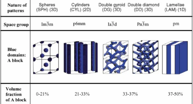
A block copolymer (BCP) can self-assemble into an ordered periodic structures with a nanometer thicknesses that depends on molecular weight, segment size, and the strength of interaction between the blocks, represented by the Flory–Huggins interaction parameter, χ. [1–3] The periodicity thickness is in the range 10–200 nm. The morphology depends on χand the composition of the copolymer, parametrized as the volume fraction of one of the constituent blocks. For the simplest class of A-B diblock copolymers, the following structures are known to be stable, as confirmed by theory [4] and experiment [2, 5]: lamellar, hexagonal-packed cylinder, body-centred cubic, close-packed spherical (which may exhibit only liquid-like ordering) and bicontinuous cubic gyroid structures, as shown in Figure 1-1. For ABC triblocks, the combination of two independent composition variables (e.g. volume fraction fA and fB, fB A+ fB+ fC
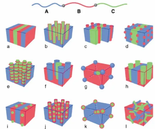
= 1) and three χ parameters (χAB, χAC and χBC) leads to a much wider range of possible morphologies shown in Figure 1-2. Many have been observed, although others await discovery. Theory provides guidelines for rationalizing the observed morphologies, and in the future may be used to predict structures.
[6]
[7]
Quantum dots have two obvious characteristics. One is the surface area effect and the other is quantum confinement effect. In surface area effect, for particles in such a small size regime, a large percentage of the atom is on or near the surface, for example, 99% of the atoms are on the surface for a 1nm size particles. [8] The existence of this vast interface between the nanoparticles and the surrounding medium can have a profound effect on the particles properties. The imperfect surface of the nanoparticles may act as electron and/or hole traps upon optical excitation. Thus the presence of these trapped electrons and holes can in turn modify the optical properties of the particles. In quantum confinement effect, “confinement” and “quantization” are two closely related definition: If a particles is “confined” then its energy is “quantized”, and vice versa. According to the dictionary, to “confine” mean to “restrict within limits” to “enclose”, and even to “imprison”. The quantum confinement not only causes the increase of the energy gap (blue shift of the absorption edge) and the splitting of the electronic states, but also changes the densities of state and the exciton oscillator strength. [9] It was revealed that many of the differences between the electronic behaviors of the bulk and the quantum-confined low-dimensional semiconductors are due to their difference densities of state.
Nanorods exhibit electronic and optical properties that differ from quantum dots. For example, unlike the spherical dots, nanorods demonstrate linearly polarized emission [10, 11] leading also to polarized lasing. [12] In addition to size and shape, nanocrystals’ charging may also significantly influence their electrical and optical properties. Millo et al. reported optical and tunneling spectroscopies on CdSe nanorods and correlated the experimental data with the level structure calculated using a multi-band effective-mass model for an infinite potential well. [13] However, the experimental set-up in both optical and tunneling measurements was tuned so as to avoid nanorods charging.
Metal nanoparticles in the diameter range 1-10 nm (intermediate between the size of small molecules and that of bulk metal) would display electronic structures, reflecting the electronic band structure of the nanoparticles, owing to quantum-mechanical rules. [14] The resulting
physical properties are neither those of bulk metal nor those of molecular compounds, but they strongly depend on the particle size, interparticle distance, nature of the protecting organic shell, and shape of the nanoparticles. [15] The few “last metallic electrons” are used for tunneling processes between neighboring particles, an effect that can be detected by impedance measurements that distinguish intra- and intermolecular processes.
Block copolymers are versatile platform materials because they can self-assemble—if they have appropriate compositions and are subjected to suitable conditions—into various nanostructures having period thicknesses between 10 and 100 nm through microphase separation of incompatible blocks. Nanostructured block copolymers can be used as templates for selectively controlling the spatial position of nanostructured materials within one of the blocks.
Zero-dimensional nanostructures, such as quantum dots and nanoparticles, have diameters in the range of 1–10 nm are the subject of much current research interest because the optical, electronic, and chemical properties of these materials. As a result, such nanostructures are being investigated for use in various applications, including light-emitting diodes, solar cells, lasers, transistors, memory cells, biological sensors, and catalysts. In these applications, the quantum dots or nanoparticles are often capped with organic ligands or are surrounded by other dielectric materials. Thus, an understanding of the collective electron transport of quantum dots or nanoparticles dispersed in organic or dielectric materials is of both scientific and technological importance. In the present study, we prepared self-assembled thin films that consisted of CdSe quantum dots or Au nanoparticles sequestered in a poly(4-vinylpyridine) nanodomain of poly(styrene-b-4-vinylpyridine) diblock copolymer and investigated the collective electron transport of the structures.
Moreover, the unique optical and electrical properties of one-dimensional (1D) semiconductor nanostructures, such as nanorods and nanowires, can be exploited for use in a number of applications. To take full advantage of the material properties of these 1D nanostructures, they must be pre-aligned or ordered in some other way. Although there are many bottom-up growth techniques for preparing 1D nanostructures in the out-of-plane 2D arrays and many techniques for pre-synthesized NRs in the in-plane 2D arrays, finding techniques for arranging pre-synthesized nanorods in out-of-plane 2D arrays remains a great challenge. The powerful aligning force of an electric field can be used to manipulate the orientation of anisotropic materials by taking advantage of their different anisotropic dielectric constants. In this thesis, we applied an electric field to induce the orientation of CdSe nanorods that had been self-assembled in the poly(4-vinylpyridine) nanodomains of a poly(styrene-b-4-vinylpyridine) diblock copolymer thin film.
Figure 1-1 Schematic phase diagram showing the various ‘classical’ block copolymer morphologies adopted by linear diblock copolymer. [6]
Figure 1-2 Schematic of morphologies for linear ABC triblock copolymer. A combination of block sequence (ABC, ACB, BAC), composition and block molecular weights provides an enormous parameter space for the creation of new morphologies. [6]
Chapter 2
Enhanced Collective Electron Transport by CdSe Quantum Dots Self-Assembled in the Poly(4-vinylpyridine) Nanodomains of a Poly(styrene-b-4- vinylpyridine) Diblock
Copolymer Thin Film 2-1 Introduction
For semiconductor nanoparticles (NPs), quantum dots (QDs), that have sizes close to their Bohr exciton radius (typically between 1 and 10 nm), their size-dependent band gaps result in tunable optical properties. [16] As a result, they possess a wide range of electrical and optical properties and can be used for various applications, such as light-emitting diodes, solar cells, lasers, and transistors. In these applications, composite materials involving nanoparticles and other organic materials were often adopted. Thus, an understanding of the collective electron transport of QDs dispersed in the organic materials is of both scientific and technological importance. A number of reports have described the three- and two-dimensional electron transport in ordered arrays of Au NPs/SiO2 superlattices, [17] ZnO QDs assemblies, [18] and organically capped CdSe QDs.[19] In addition, electron transport also has been examined in granular films of Au NPs linked by alkanethiol molecules[20] or poly(4-vinylpyridine)[21] and Au/spacer/CdSe QD[22] assemblies. Orbital-selective electron transport through a single CdSe QD measured with an STM has also been reported.[23]
Thin films of diblock copolymers are versatile templates for the preparation of long-range-ordered nanostructures of dots because their periodic thicknesses can be tuned between 10 and 100 nm. [24] For example, the selective sequestration of pre-synthesized CdS, [25a] CdSe[26] and TiO2[25b] nanoparticles into one block of diblock copolymers are performed by ensuring the presence of strong interactions between one block of a diblock copolymer and the surface ligands of the nanoparticles. An assembly of Au nanoparticles enclosed by a block copolymer has also been reported. [27] In the present study, we prepared self-assembled thin films that consisted of CdSe QDs sequestered in a poly(4-vinylpyridine) nanodomain of poly(styrene-b-4-vinylpyridine) (S4VP) diblock copolymer, following a previous approach. [25] By conductive atomic force microscopy (C-AFM) and device measurements, we found that the electron tunneling rate constant in the case of CdSe QDs confined in a poly(4-vinylpyridine) nanodomain is much larger than that in the randomly distributed case. To our knowledge, this is the first time the nanodomain confined effect on the collective electron transport behavior of quantum dots has been reported. This work has great implications on hybrid photovoltaic cell or light-emitting diode applications because collective electron transport by CdSe QDs and hole transport by organic materials, respectively, are critical for producing highly efficient hybrid photovoltaic cell [16] or light emitting diode. [28]
2-2 Methods and Analysis
2-2-1 Materials. The poly(styrene-b-4-vinylpyridine) (S4VP) diblock copolymer and the poly(4-vinylpyridine) homopolymer were purchased from Polymer Source, Inc. The polydispersity index (Mw/Mn) was 1.23, and the molecular weights (Mn) of the PS and P4VP blocks were 365,300 and 29,400 g/mol, respectively. Cadmium oxide (CdO, 99.9%), selenium (Se, 99.9%, 100 mesh), and trioctylphosphine (TOP) were obtained from Aldrich.
Trioctylphosphine oxide (TOPO), 1-octadecene (ODE), and n-hexadecylamine (HDA) were purchased from Lancaster. Stearic acid (99%, Avocado), hexane (99%, TEDIA USA), toluene (99%, TEDIA USA), methyl alcohol (MeOH, 99%, TEDIA USA), and pyridine (99%, Showa) were obtained from commercial sources.
2-2-2 Synthesis of CdSe/TOPO QDs. CdSe QDs were synthesized using a modification of a procedure reported previously. [29] First, a mixture of CdO (0.2 mmol), stearic acid (0.8 mmol), and ODE (2 g) was heated in a 25 mL three-neck flask to ca. 200 °C to obtain a colorless, clear solution. After this solution had cooled to room temperature, HDA (1.5 g) and TOPO (0.5 g) were added to the flask. This system was then reheated to 280 °C under an argon flow. At this temperature, a selenium solution, prepared by dissolving Se (2 mmol) in TOP (1 mL), was injected rapidly. The growth temperature was reduced to 250 °C for 30 s and then the reaction mixture was cooled to room temperature. The dots were collected as powders using size-selective precipitation with methanol and then redispersed in toluene.
2-2-3 Preparation of CdSe/pyridine QDs. CdSe/TOPO powder (30 mg) was dissolved in pyridine (5 mL) and then stirred at 65 °C for 6 h. Hexane (30 mL) was added to reprecipitate the CdSe. The orange/red suspension was centrifuged and then the powder was collected and redissolved in pyridine.
2-2-4 Preparation of bulk (CdSe/P4VP)-b-PS. PS-b-P4VP (0.05 g) was added to pyridine (1 mL). Samples of 10, 15, 26, 33, and 48% CdSe/pyridine (with respect to the volume fraction of P4VP block) were mixed in the PS-b-P4VP/pyridine polymerization solution. These mixtures were dried slowly under vacuum at 50 °C and then maintained at 160 °C for 48 h to obtain the bulk (CdSe/P4VP)-b-PS composites.
2-2-5 Preparation of thin films of (CdSe/P4VP)-b-PS. Micellar solutions (0.5 wt%) of (CdSe/P4VP)-b-PS were prepared by dissolving bulk (CdSe/P4VP)-b-PS in toluene. The micellar solutions were spin-coated at 5000 rpm for 60sec on carbon-coated silicon wafers for transmission electron microscopy (TEM), and Pt-coated wafer for conductance atomic force microscopy (C-AFM) and device measurement. We prepared the sample of CdSe distributed in P4VP homopolymer under the same conditions we had used to prepare (CdSe/P4VP)-b-PS, including the amount of CdSe in P4VP and the thickness of the thin CdSe/P4VP film.
2-2-6 Characterization. TEM images were obtained using a JOEL-2010 transmission electron microscope. The thin film sample for TEM was prepared by using 1% HF to remove it from the carbon-coated silicon wafer. C-AFM measurements were performed using a Digital Nanoscope IV3100 under ambient conditions. The current-voltage (I-V) characteristics of device of thin films of (CdSe/P4VP)-b-PS was measured by Hewlett-Packard 4156B. Using a base pressure below 1 × 10⁻⁶ Torr, a layer of Al (100nm) was vacuum deposited as top electrode. UV–Vis absorption spectra were obtained on an Aglient 8453 spectrometer by scanning between 190 and 1000 nm. Photoluminescence spectra (PL) were obtained at room temperature using a Hitachi F4500 fluorescence spectrophotometer. The concentrations of the CdSe/TOPO in toluene and CdSe/pyridine solutions were diluted to 6 × 10⁻⁵ M for the UV–Vis and PL spectroscopy experiments. Small-angle X-ray scattering experiments were performed on a wiggler beamline BL-01B1 at the National Synchrotron Radiation Research Center, Taiwan. The cyclic voltammetry (CV) curve of pure P4VP was measured by coating the polymer onto a Pt plate and using a standard calomel electrode as the reference and 0.1 M (n-Bu)4NBF4/acetonitrile as the
electrolyte; the scanning rate was set to 50 mV/sec.
2-3 Results and Discussions
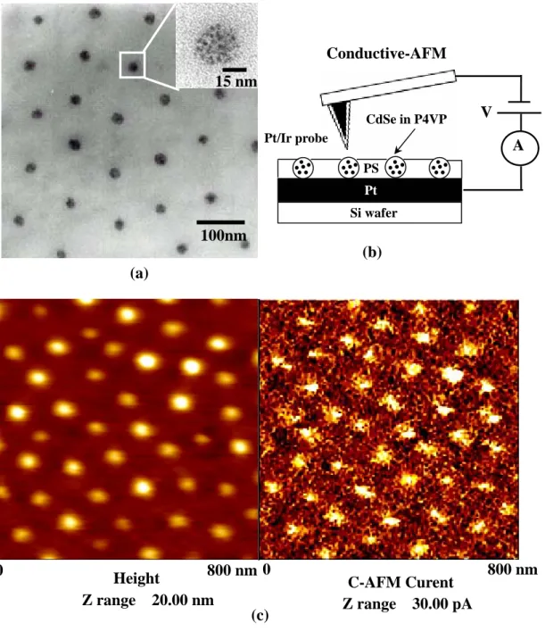
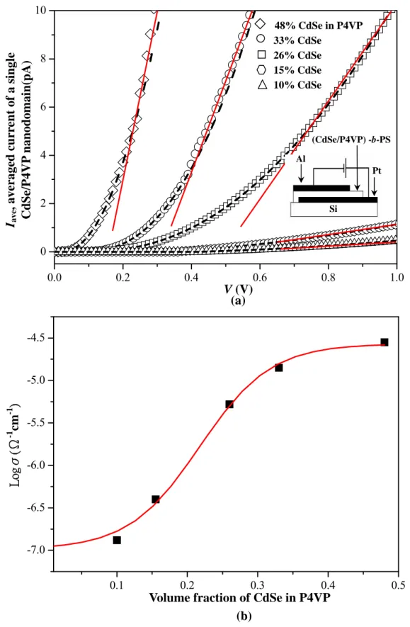
Scheme 2-1 demonstrates the process for preparing a mono-layered (CdSe/P4VP)-b-PS thin film. First, the TOPO ligands on CdSe QDs were exchanged by hydrophilic pyridine ligands. Then, pyridine-modified CdSe QDs and PS-b-P4VP block copolymer are dissolved and mixed in pyridine, and CdSe QDs are distributed selectively in the P4VP phase due to the dipole-dipole interactions. After drying, (CdSe/P4VP)-b-PS in bulk form was obtained. Subsequently, toluene, which is a good solvent for PS but a poor one for P4VP, is used to form a solution containing micelles of CdSe/P4VP-core and PS-shell. Figure 2-1a displays the transmission electron microscopy (TEM) image of a thin film of 48% (CdSe/P4VP)-b-PS obtained without staining. The dark region represents the CdSe/P4VP composite phase (because of the higher electron density of cadmium). The spherical nanostructure of PS-b-P4VP is, therefore, revealed clearly. The diameter of the CdSe/P4VP sphere was ca. 35 nm, and the inter-domain distance was ca. 100 nm. The inset of Figure 2-1a reveals that CdSe QDs were dispersed homogeneously in the P4VP nanodomain. Figure 2-1b displays a schematic representation of the C-AFM method we used to analyze the CdSe/P4VP spheres embedded in the polystyrene. The current image was measured at the sample bias of VB = 8 V. Figure 2-1c presents the topographic and current images of a section of the thin film of 48% (CdSe/P4VP)-b-PS. In the height image, the light regions having a size of ca. 35 nm represent the CdSe/P4VP domains, while the dark area represents the polystyrene matrix. Because the thickness of the thin film is smaller than the size of the CdSe/P4VP domain (23 vs. 30 nm), this image indicates that the microphase-separated (CdSe/P4VP)-b-PS exists as a monolayered thin film. In the current image, the values of the currents of the P4VP/CdSe phases (light region) were ca. 30–40 pA, whereas that of the PS phase (dark region) was at the level of the noise (ca. 0.5 pA).
Figure 2-2a displays the current–voltage (I–V) curves of a single CdSe/P4VP nanodomain as measured by C-AFM. The turn-on voltages for the CdSe/P4VP nanodomain decreased as the number of incorporated CdSe QDs increased. This phenomenon occurs because the electron mobility from the probe to the nanodomain increased upon increasing the density of the CdSe QDs. The linear regions of the I-V curves represent the Ohmic behavior, [30] and indicate constant conductivities ( ) that can be calculated from the slope of the curves. σ [31] The nonlinear regions were due to the electron tunneling from probe tip to the conduction band of CdSe QDs, which must overcome the barrier height (φe) of the P4VP between the tip and CdSe (Inset of Figure 2-2a). [31, 32a] A tunneling process, in which electron injection occurs under a forward bias, can be properly modeled using the Fowler–Nordheim (FN) equation. The FN equation can be used to determine the electron barrier height (φe). [31] The φe values for the 10, 15, 26, 33, and 48% CdSe QDs in the P4VP block were 2.4, 2.2, 2.0, 1.8, and 1.5 eV, respectively. [31] The electron barrier height (φe) decreases monotonically when the amount of CdSe QDs in the P4VP block increases, owing to the fact that the distance between tip and CdSe QDs decreased at higher CdSe QDs densities. Figure 2-2b displays the conductivity of a single CdSe/P4VP nanodomain plotted against the volume fraction of incorporated CdSe in P4VP. The conductivity of the CdSe/P4VP nanodomain displays only a slight change at low CdSe loading, exhibits a sharp increase at a critical loading, and becomes saturated at high loading.
Hence, the conductivity of polymers incorporating CdSe QDs is best described by a percolation theory (the solid curve in Figure 2-2b represents the best fit to the experiment data). [31] Table 2-1 lists the conductivity of a single CdSe/P4VP nanodomain of the samples, σ , as ranging from 10–5 to 10–7 Ω cm–1 –1. The conductivity (σ ) increases as the amount of CdSe increased, owing to the fact that the distance between CdSe QDs decreased at higher CdSe QDs densities. We also obtained the averaged current–voltage (Iave–V) curves of a single CdSe/P4VP nanodomain in PS matrix by a sandwiched device. [31] The conductivity (σ ) also increases as the amount of CdSe increased and is of the same order of magnitude as compared to that by C-AFM measurement, ranging from 10–5 to 10 Ω cm–7 –1 –1, given in Table 2-1.
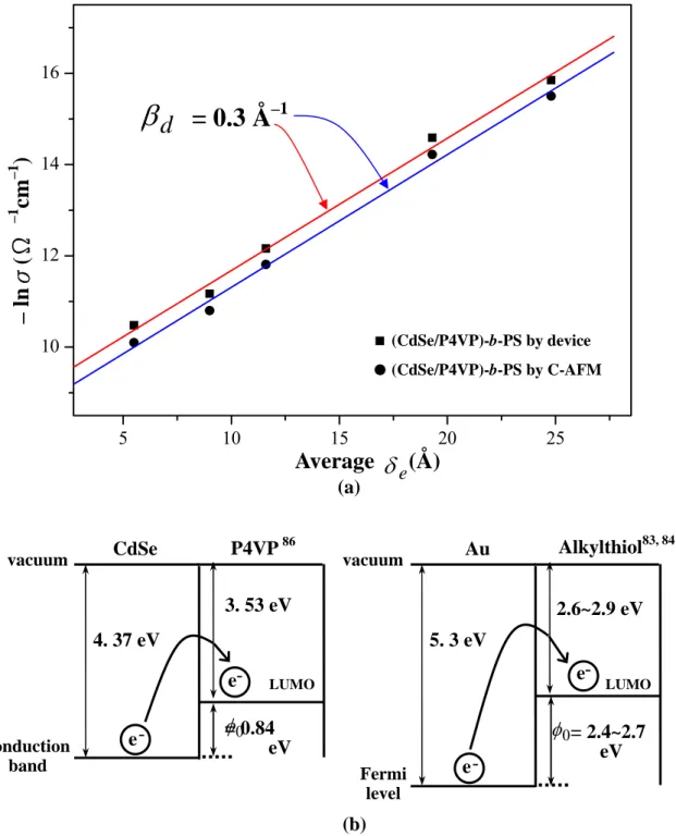
Figure 2-3a displays a plot of –ln (σ ) vs. the edge-to-edge interparticle distance (δe) as measured by C-AFM and in a device. The conductivity in terms of δe and temperature (T ) is described [20, 33] by Eq. (2-1):
(
)
=[
−]
⎢⎣⎡ − ⎥⎦⎤ RT E T d e A e, σ0 exp β δ exp δ σ (2-1)where σ is the value of the conductivity of the resulting composite, βd is the electron tunneling coefficient, δe is the edge-to-edge interparticle distance, [31] is the activation barrier energy, R is the gas constant, and
A E
T is the temperature. The linear slope in the plot of –ln (σ ) vs. δe indicates an electron hopping mechanism and the value of the slope (i.e., βd) is 0.3 Å–1. In our system, the value of βd differs from that found in other cases. For instance, the value of βd is 0.2–0.6 Å–1 for electron tunneling through π-bonded molecules, and ca. 0.6–1.0 Å–1 for saturated molecules. [34] The electron tunneling coefficient βd can be described [34] by Eq. (2-2): 2 * 0 2 2 h
φ
β
d = m (2-2)where m* is the electron effective mass, 0
φ
is the electron tunneling barrier height between the dots, and is the reduced Planck constant. Electron tunneling from one dot to the next must overcome the tunneling barrier height (h
0
φ
) of the spacer between the two dots. We found that the value of βd in the CdSe-P4VP-CdSe system (0.3 Å–1) is small when compared to that in the Au-alkanethiol-Au system (0.8–1.2 Å–1), because the tunneling barrier height between the conduction band of CdSe and the lowest unoccupied molecular orbital (LUMO) of P4VP is smaller than that between the Fermi level of Au and the LUMO of an alkanethiol (Figure 2-3b).[20, 21] The smaller βd value for (CdSe/P4VP)-b-PS than that for Au-alkanethiol indicates that the edge-to-edge interparticle distance has less effect on the conductivity for (CdSe/P4VP)-b-PS than for the Au-alkanethiol-Au system. The effective electron mass, m*=0.14m, was calculated by Eq. (2-2). Where mis the free electron mass.To compare the effect that nanodomain confinement has on the CdSe QDs, with respect to their randomly distributed state, we prepared four samples that had the same density in P4VP: the first two contained 48% CdSe by volume with respect to the P4VP block in a PS-b-P4VP diblock copolymer and the second two contained 48% CdSe by volume in a P4VP homopolymer. The electron tunneling rate constant (kET) can be estimated from the conductivity by assuming a
cubic-lattice model describedby an equation. [20, 31] Table 2-1 indicates that both the electron tunneling rate constant and conductivity for the nanodomain confined case is about seven times larger than that for the randomly distributed case. This can be explained by the fact that the collective electron transport of CdSe QDs in the nanodomain confined case was restricted by the P4VP sphere, while the collective electron transport for the randomly distributed CdSe QDs followed a free pathway behavior. The electron tunneling rate constant increased as the amount of CdSe increased.
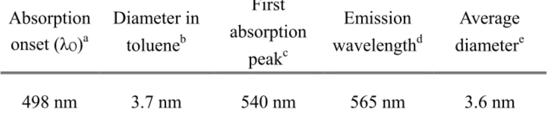
Table 2-2 displays the characteristic properties of CdSe QDs. The average size of the CdSe QDs was determined from both UV–Vis absorption spectroscopy and transmission electron microscopy measurements to be ca. 3.6 nm.
The FN equation can be expressed [32] as Eq. (2-3):
⎥ ⎥ ⎦ ⎤ ⎢ ⎢ ⎣ ⎡− = E q h m m h m E q A C I e e eff 3 * 2 8 exp * 8 ) ( 2 / 3 2 3 π φ φ π (2-3) E
where Aeff is the effective contact area, is the applied electric field, φe is the electron barrier height, and and are electron charge, effective mass of the electron, free electron mass, and Plank constant, respectively. If we assume
, *, ,m m q h L V E= / , where V is the
applied voltage, and Lis the separation between the two electrodes, then I(V)= DV2exp(−B/V) 2 / 3 2 / 1 2 / 3 * 83 . 6 3 * 2 8 e e m m L q h L m B π φ ⎟ φ ⎠ ⎞ ⎜ ⎝ ⎛ = = * 8 2 3 m L h m q A D e eff φ π = ,and (volts) where
Here the units of Land φeare nm and eV, respectively. By fitting the measured I-V curves to FN theory, the B for the 10, 15, 26, 33, and 48% CdSe QDs in the P4VP block were 284.8 V, 249.9 V, 216.6 V, 184.9 V, and 140.7 V, respectively. Using the fitted B values and the thickness between two electrodes of ~30 nm, theφe for the 10, 15, 26, 33, and 48% CdSe QDs in
the P4VP block were , , , , and
eV, respectively. The effective electron mass, 3 / 1 ) / ( 24 . 1 m m* 1.14(m/m*)1/3 1.03(m/m*)1/3 0.93(m/m*)1/3 3 / 1 ) / ( 77 . 0 m m* m*=0.14m, was calculated by
Eq. (2-2). Theφe for the 10, 15, 26, 33, and 48% CdSe QDs in the P4VP block were 2.4, 2.2, 2.0, 1.8, and 1.5 eV, respectively.
Additionally, we calculated the conductivity values using Eq. (2-4):
A L R× = 1 σ (2-4) R
where is the resistance, is the thickness between two electrodes, and L A is the contact area of the electrode. In this case, is equal to the diameter of the nanodomain, and L A is defined by the contact area between the tip and the sample, 100 nm2. [35]
The percolation model for the conductivity of CdSe/P4VP is given in Eq. (2-5), which provides [21] a first-order approximation:
(
) (
[
) (
)
]
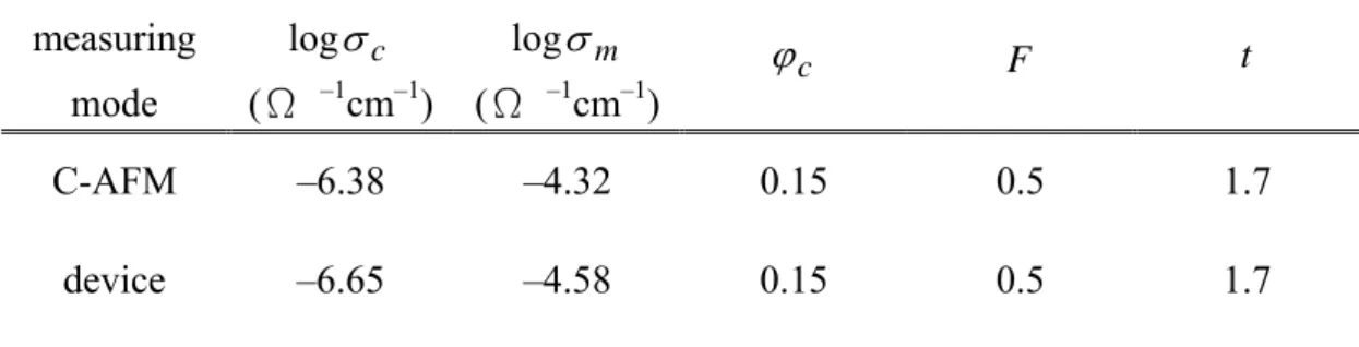
t c c c m c σ σ ϕ ϕ F ϕ σ σ = + − − / − (2-5)conductivity at the percolation threshold, σm is the maximal conductivity value, ϕ is the volume fraction of QDs, ϕc is the critical volume fraction, F is the limiting value of the volume fraction, and is the critical exponent. Table 2-3 lists the corresponding parameters for C-AFM and device measurements.
t
Figure 2-4a displays the averaged current–voltage (Iave–V) curves of a single CdSe/P4VP nanodomain in PS matrix derived from the measurement of a sandwiched device, in which a Pt-coated Si wafer as the bottom electrode and Al film as the top electrode. The current was assumed to flow through CdSe/P4VP nanodomain, owing to a much higher resistance of PS phase. The current density of a single nanodomain can therefore be calculated from the density of CdSe/P4VP nanodomain in PS phase by using the following parameters, where the area of Al electrode is 1.96 × 10⁻³ cm2; the density of CdSe/P4VP nanodomain in PS phase is 3.1 × 109 cm-2 as obtained from TEM image. The number of CdSe/P4VP nanodomains under the Al electrode is a product of the area of Al electrode and the density of CdSe/P4VP nanodomains, which is about 6 × 10⁶. The Iave is obtained by dividing the current by the number of CdSe/P4VP nanodomains and then by the area of a CdSe/P4VP nanodomainan. Similar to the results by conductive-AFM, the turn-on voltages for the CdSe/P4VP nanodomain decreased as the number of incorporated CdSe QDs increased. Figure 2-4b displays the conductivity plotted against the volume fraction of incorporated CdSe in P4VP. The electron barrier height (φe), determined by Eq. (2-3), from the Al electrode to the nanodomain decreases monotonically when the amount of CdSe increases. We also calculated the conductivity values using the linear region of Iave–V curves by Eq. (2-4). The solid curve in Figure 4b represents the best fit of percolation model, Eq. (2-5), to the experiment data; Table 3 lists the corresponding parameters.
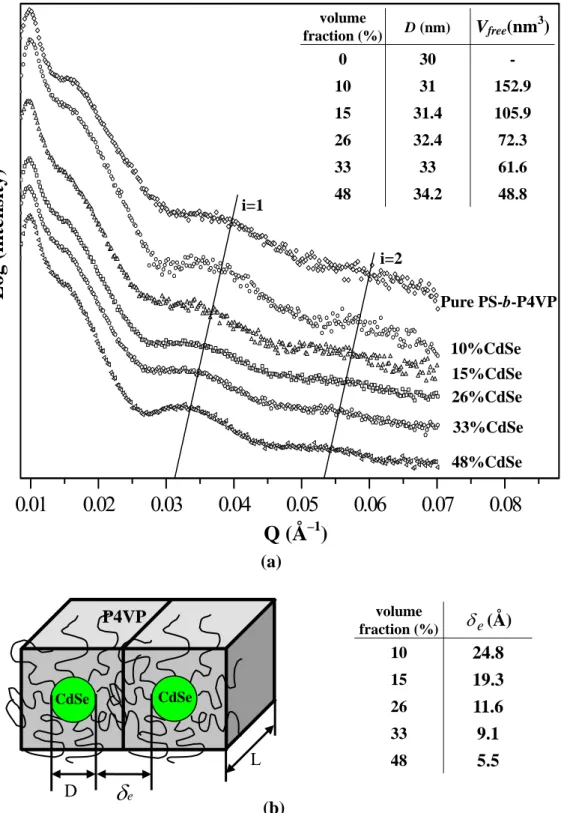
Figure 2-5a displays one-dimensional small-angle X-ray scattering patterns (SAXS) of (CdSe/P4VP)-b-PS obtained using synchrotron radiation. The scattering maxima, which are denoted by the letter “i” (i = 1, 2), are form factor peaks associated with scattering from the isolated spherical domains. The form factor peaks shifted slightly to lower values of Q as the amount of incorporated CdSe increased, which indicates that the volume or size of the CdSe/P4VP composite domains increased. The average diameter of the P4VP domains of pure PS-b-P4VP, deduced from the positions of the form factor maxima, is 30 nm. The average diameters, measured by their volume, for the 10, 15, 26, 33, and 48% CdSe QDs in the P4VP block were 31, 31.4, 32.4, 33, and 34.2 nm, respectively, assuming that the density of P4VP and CdSe remained the same before and after mixing. Inset of Figure 2-5a lists the free volume per CdSe dot in a single P4VP domain ( ), which is defined by the average volume of an occupied CdSe dot and can be estimated by using Eqs. (2-6) and (2-7):
free V n V V V CdSe VP P VP P CdSe/ 4 − 4 = (2-6) free VP P CdSe V n V / 4 = (2-7)
where is the volume of a single CdSe/P4VP composite domain, is the volume of a single P4VP domain, is the volume of a CdSe QD, and is the maximum number of
VP P CdSe V / 4 VP4VP CdSe V n
CdSe QDs in a single P4VP domain. The relationship between the conductivity and the edge-to-edge interparticle distance (δe) can be determined by assuming a cubic lattice model for the CdSe QDs. The values of δe were calculated using Eq. (2-8) based on the cubic lattice model presented in the Figure 2-5b. [20, 31]
(
V)
D D L free e = − = − 3 / 1 δ (2-8)where D is the diameter of the CdSe QDs. The value of δe decreased when the amount of CdSe increased, as displayed in the inset of Figure 2-5b.
The first-order electron tunneling rate constant ( ) can be estimated from the conductivity by assuming a cubic-lattice model described
ET k [20, 33] by Eq. (2-9):
( )
C F RT s k c a ET 1 2 2 6 δ σ = − (2-9)R is the gas constant, T is the temperature,
where σ is the conductivity, is the
Faraday constant,
a
F is the average center-to-center interparticle distance ( =
c
δ δc δe+ 32 Å), and
is the concentration of CdSe in the P4VP domain (mol/cm3
C ).[36]
2-4 Conclusions
We have demonstrated that the electron tunneling rate constant in the case of CdSe QDs confined in a poly(4-vinylpyridine) nanodomain is much larger than in the randomly distributed case and it increases upon increasing the amount of CdSe. The value of electron tunneling coefficient of the CdSe-P4VP-CdSe system is 0.3 Å–1. The electron barrier height from the tip of the probe to the nanodomain decreased monotonically and the conductivity of the CdSe/P4VP nanodomain increased, following a percolation model, as the amount of CdSe increased.
Scheme 2-1: Fabrication of a self-assembled (CdSe/P4VP)-b-PS thin film by incorporating selectively dispersed pre-synthesized CdSe QDs in P4VP domain.
PS PS Micellar (CdSe/P4VP)-b-PS in pyridine Mono-layered film of (CdSe/P4VP)-b-PS drying CdSe in P4VP PS P4VP N N N N N N N N CdSe O P O P O P O P O P O P (TOPO) py CdSe O P O P ridine toluene PS PS PS Bulk spherical CdSe/P4VP in PS matrix
Table 2-1: Conductivity (σ ) and electron tunneling rate constant ( ) for confined and non-confined CdSe in P4VP domain as measured by conductive-AFM and in a device.
ET k σ (Ω-1cm-1) × 106 ET k (s-1) × 10–3 (CdSe/P4VP)-b-PS (confined) CdSe/P4VP (non-confined) (CdSe/P4VP)-b-PS (confined) CdSe/P4VP (non-confined) vol% of CdSe in P4VP
C-AFM device C-AFM device C-AFM device C-AFM device 10 0.2 0.13 0.03 0.01 1.4 0.9 0.2 0.09 15 0.6 0.46 0.08 0.05 4.2 3.2 0.5 0.4 26 7.4 5.2 0.82 0.6 39 27 4.3 3.1 33 20 14 2.2 1.6 87 60 9.6 6.9
Table 2-2: Characteristic Properties of CdSe Quantum Dots First absorption peak Absorption onset (λo) Diameter in toluene Emission wavelength Average diameter a b d e c 498 nm 3.7 nm 540 nm 565 nm 3.6 nm
a The onset absorption wavelength of CdSe QDs in toluene as obtained from UV–Vis spectra. b The sizes of the CdSe QDsin toluene were calculated using the onset absorption obtained from UV–Vis spectra and the following equation:
R e R Eg Eg Egos ref ε μ π 2 2 2 2 1 1.8 2 • − ≈ Δ = − h
c The first exitonic absorption wavelength of CdSe QDs in toluene as obtained from UV–Vis spectra.
d The emission wavelength was determined from the photoluminescence measurements. e The sizes of the CdSe QDs were determined from TEM analyses.
Table 2-3: Electrical conductivity parameters for the CdSe/P4VP nanodomain
measuring logσc logσm t
c ϕ F –1 mode (Ω cm–1) (Ω cm–1 –1) C-AFM –6.38 –4.32 0.15 0.5 1.7 device –6.65 –4.58 0.15 0.5 1.7
(a) 100nm 15 nm V A Si wafer CdSe in P4VP PS Pt/Ir probe Pt (b) Conductive-AFM 0 800 nm 0 800 nm
Height C-AFM Curent
Z range 20.00 nm Z range 30.00 pA (c)
Figure 2-1: (a) TEM image of a thin film of 48% (CdSe/P4VP)-b-PS obtained without staining. (b) A schematic representation of the conductive-AFM imaging mode employed. (c) Conductive-AFM image of a thin film of 48% (CdSe/P4VP)-b-PS.
0 5 10 15 20 25 30 0.1 0.2 0.3 0.4 0.5 -6.5 -6.0 -5.5 -5.0 -4.5 Log σ (Ω -1 cm -1 )
Volume fraction of CdSe in P4VP (b) 0 1 2 3 4 5 6 7 (a) V (V) I, curr ent of a single C dSe/P4VP
nanodomain (pA) by C-AFM
48% CdSe in P4VP 33% CdSe 26% CdSe 15% CdSe 10% CdSe Pt substrate tip CdSe valence band conduction band Ef Ef - + P4VP e φ e φ eVa
Figure 2-2: (a) I–V curves of thin film (CdSe/P4VP)-b-PS by conductive-AFM. The dotted lines denote best fits to the FN equation. Inset: The energy bands of the conductive-AFM tip, CdSe/P4VP monolayer, and the substrate. Ef is the electron Fermi energy inside the Pt, and φe is the barrier height between Pt and CdSe/P4VP. eVa is the applied potential energy difference between the tip and the substrate. (b) Plot of the conductivity vs. the amount of CdSe in P4VP.
5 10 15 20 25 10 12 14 16
= 0.3 Å
–1 (a)– ln
σ
(Ω
– 1cm
– 1)
Average (Å)
eδ
(CdSe/P4VP)-b-PS by device (CdSe/P4VP)-b-PS by C-AFMd
β
conduction band vacuum P4VP 86 LUMO 3. 53 eV CdSe 4. 37 eV = 0.84 eV e- e- φ0 (b) Fermi level vacuum Alkylthiol 83, 84 LUMO 2.6~2.9 eV Au 5. 3 eV = 2.4~2.7 eV e-e - 0 φFigure 2-3: (a) Plot of –ln(σ (CdSe/P4VP)-b-PS) vs. δe as measured by conductive-AFM and device. (b) Schematic diagram of the barrier height for electron tunneling from the conduction band of CdSe to the LUMO of P4VP and from the Fermi level of Au to the LUMO of an alkanethiol.
0.1 0.2 0.3 0.4 0.5 -7.0 -6.5 -6.0 -5.5 -5.0 -4.5 Logσ( Ω -1 cm -1 )
Volume fraction of CdSe in P4VP (b) 0.0 0.2 0.4 0.6 0.8 1.0 0 2 4 6 8 10
Figure 2-4: (a) Iave–V curves of thin film (CdSe/P4VP)-b-PS nanocomposites having various
contents of CdSe as measured in a device. The dotted lines denote best fits to the FN equation. (b) Plot of the conductivity vs. the amount of incorporated CdSe in P4VP.
(a) V (V) Iave CdSe/P4VP nanodomain(pA) , averaged curr ent of a single Pt Al (CdSe/P4VP) -b-PS Si 48% CdSe in P4VP 33% CdSe 26% CdSe 15% CdSe 10% CdSe
volume fraction (%)
Figure 2-5: (a) Small-angle X-ray scattering of bulk (CdSe/P4VP)-b-PS nanocomposites having various contents of CdSe. (b) A schematic representation of the cubic lattice model for the free volume per CdSe dot in a single P4VP domain.
D (nm) Vfree(nm )3 0 30 - 10 31 152.9 15 31.4 105.9 26 32.4 72.3 33 33 61.6 48 34.2 48.8 volume fraction (%) δe(Å) 10 24.8 15 19.3 26 11.6 33 9.1 48 5.5
0.01
0.02
0.03
0.04
0.05
0.06
0.07
0.08
i=1 i=2 Pure PS-b-P4VP 33%CdSe 26%CdSe 15%CdSe 48%CdSe 10%CdSeLog (intensity)
Q (Å
–1)
(a) (b) CdSe CdSe D L eδ
P4VPChapter 3
Collective Electron Transport in Au Nanoparticles Self-Assembled in the Poly(4-vinylpyridine) Nanodomains of a Poly(styrene-b-4-vinylpyridine) Diblock
Copolymer Thin Film 3-1 Introduction
Metal nanoparticles (NPs) that have diameters in the range of 1–10 nm are the subject of much current research interest because the optical, electronic, and chemical properties of these materials, such as their single charge tunneling and plasmon resonances, are size-dependent. [37–39] As a result, such NPs are being investigated for use in various applications, including memory cells, [40] single-electron transistors, [41] biological sensors, [42] and catalysts. [43] In these applications, the NPs are often capped with organic ligands or are surrounded by other dielectric materials. Thus, an understanding of the collective electron transport of NPs dispersed in organic or dielectric materials is of both scientific and technological importance. A number of reports have described two- or three-dimensional electron transport in (a) ordered arrays of dodecanethiol-capped Ag[44] and Au[45] nanoparticles, Au NPs/SiO2 superlattices,[46] organically capped Co NPs,[47] and CoPt3 NPs[48] and (b) disordered arrays of granular films of Au NPs linked by alkanethiol molecules[49] and Au/spacer/CdSe NP assemblies.[50] In contrast, very few reports describe one-dimensional electron transport within granular films, mainly because of the difficulties encountered when preparing such samples.
Nanostructured block copolymers that have period thicknesses between 10 and 100 nm, because of microphase separation of incompatible blocks, can be used as templates to selectively control the spatial arrangement of NPs within one of the blocks. [51–54] For example, the selective sequestration of pre-synthesized CdSe,[55a,b] CdS,[55c] and TiO2[55d] NPs into one block of a diblock copolymer can be performed by ensuring that strong interactions exist between that block of the copolymer and the surface ligands of the NPs. Block copolymers can also be used as nanoreactors for the synthesis of nanomaterials. For example, quasi-regular arrays of Au clusters[56] and TiO2 needles[55e] have been obtained through the selective sequestration of metal ions into one block of poly(styrene-b-vinylpyridine). In this present study, we followed a previously reported [55] approach to prepare self-assembled thin films that consisted of Au NPs sequestered in the poly(4-vinylpyridine) (P4VP) nanodomains of a poly(styrene-b-4-vinylpyridine) (PS-b-P4VP) diblock copolymer. From the current–voltage (I–V) characteristics of these thin films, we determine the collective electron transport behavior of the Au NPs confined within the P4VP nanodomains and of randomly distributed Au NPs.
3-2 Methods and Analysis
3-2-1 Materials. The poly(styrene-b-4-vinylpyridine) (S4VP) diblock copolymer and the poly(4-vinylpyridine) homopolymer were purchased from Polymer Source, Inc. The polydispersity index (Mw/Mn) of S4VP was 1.07; the molecular weights (Mn) of the PS and P4VP blocks were 557,000 and 75,000 g/mol, respectively. Hydrogen tetrachloroaurate(III) trihydrate (HAuCl4·3H2O), tri-n-octylammonium bromide (TOAB, 99%), and sodium borohydride (NaBH4, 99%) were obtained from Acros. Trioctylphosphine (TOP, 90%) were purchased from Aldrich. Toluene (99%, TEDIA USA), hexane (99%, TEDIA USA), methyl
alcohol (MeOH, 99%, TEDIA USA), and pyridine (99%, Showa) were obtained from commercial sources.
3-2-2 Synthesis of Au/TOP NPs. Au/TOP NPs were synthesized using a modification of a procedure reported previously. [57] First, HAuCl4
·3H2O (0.24 g, 0.616 mmol) was dissolved in deionized water (6.25 mL) in a 50-mL three-neck flask. This solution was added to a mixture of TOAB (0.39 g, 0.711 mmol) in toluene (8.125 mL) and stirred vigorously. Once all of the color has transferred from the aqueous layer into the organic phase, a solution of TOP (0.20 mL, 0.43 mmol) in toluene (2 mL) was injected into the reaction mixture. The organic phase turned bright red; neat TOP was then slowly added dropwise until the mixture turned a milky white color. A solution of NaBH4 (88.0 mg, 2.33 mmol) in deionized water (5 mL) was then added to the mixture at a nominal rate of 7 mL/h using a syringe pump. Upon addition, the organic phase immediately darkened, progressively turning a deeper brown/black color. After the complete addition of NaBH4, the reaction mixture was stirred for 30 min. The nanoparticles were collected as a powder through size-selective precipitation with methanol and then they were redispersed in toluene.
3-2-3 Preparation of Au/Pyridine NPs. The Au/TOP NP powder (30 mg) was dissolved in pyridine (5 mL) and then stirred at 65 °C for 6 h. Hexane (30 mL) was added to reprecipitate the Au NPs. The suspension was centrifuged and then the powder was collected and redissolved in pyridine.
3-2-4 Preparation of Bulk (Au NPs/P4VP)-b-PS. PS-b-P4VP (0.05 g) was added to pyridine (1 mL). Samples of 10, 15, 26, 33, and 48% Au/pyridine (percentages with respect to the volume fraction of P4VP block) were mixed in the PS-b-P4VP/pyridine polymerization solution. These mixtures were dried slowly under vacuum at 50 °C and then maintained at 160 °C for 48 h to obtain the bulk (Au NPs/P4VP)-b-PS composites.
3-2-5 Preparation of Thin Films of (Au NPs/P4VP)-b-PS. Micellar solutions (0.5 wt%) of (Au NPs/P4VP)-b-PS were prepared by dissolving bulk (Au NPs/P4VP)-b-PS in toluene. The micellar solutions were spin-coated at 5000 rpm for 60 s onto carbon-coated silicon wafers [for transmission electron microscopy (TEM)] and Au-coated wafers [for current-voltage (I–V) curves measurements]. The sample of Au NPs distributed in the P4VP homopolymer was prepared under the same conditions used to prepare (Au NPs/P4VP)-b-PS, including the amount of Au in P4VP and the thickness of the thin Au NPs/homo-P4VP film.
3-2-6 Preparation of a Sample for Cross-Sectional TEM Imaging. A micellar solution of 48% (Au NPs/P4VP)-b-PS in toluene was spin-coated at 5000 rpm for 60 s onto a Au-coated polyethersulfone substrate; a layer of Au (200 nm) was then vacuum-deposited as the top electrode. The sandwiched sample was placed into an epoxy capsule, which was cured at 70 °C for 48 h in a vacuum oven. The cured epoxy samples were microtomed using a Leica Ultracut Uct into ca. 50-nm-thick slices.
3-2-7 Characterization. TEM images were obtained using a JOEL-2010 transmission electron microscope. The thin film sample for TEM was obtained after using 1% HF to remove the film from the carbon-coated silicon wafer. The current–voltage (I–V) characteristics of the thin film device of (Au NPs/P4VP)-b-PS were measured using a Hewlett–Packard 4156B instrument. Using a base pressure below 1 × 10⁻⁶ torr, a layer of Au (100 nm) was vacuum-deposited as the top electrode. Small-angle X-ray scattering experiments were performed on a wiggler beamline
BL-01B1 at the National Synchrotron Radiation Research Center (NSRRC), Taiwan.
3-3 Results and Discussions
Scheme 3-1 outlines our approach toward preparing a monolayer (Au NPs/P4VP)-b-PS thin film. First, the trioctylphosphine (TOP) ligands on the Au NPs, which were used during their synthesis, were replaced with hydrophilic pyridine ligands. These pyridine-modified Au NPs and the PS-b-P4VP block copolymer were then dissolved and mixed in pyridine; the Au NPs were distributed selectively in the P4VP phase as a result of dipole–dipole interactions. After drying, the (Au NPs/P4VP)-b-PS sample was obtained in bulk form. Subsequently, toluene, which is a good solvent for PS but a poor one for P4VP, was used to form micelles—having Au NPs/P4VP cores and PS shells—in a solution that was spun into a thin film. Figure 3-1a displays a transmission electron microscopy (TEM) image, obtained without staining, of the top view of a thin film of 48% (Au NPs/P4VP)-b-PS. The dark region represents the Au NPs/P4VP composite phase (because of the higher electron density of gold). It is clear that PS-b-P4VP had a spherical nanostructure. The diameter of the Au NPs/P4VP sphere was ca. 30 nm, and the inter-domain distance was ca. 90 nm. Figure 3-1b displays an HRTEM image of a single Au NPs/P4VP nanodomain within a thin film of 48% (Au NPs/P4VP)-b-PS. The Au NPs were dispersed fairly homogeneously in the P4VP nanodomain. The inset of Figure 3-1b reveals the HRTEM lattice image (with a lattice spacing of ca. 2.8 Å) of one of the Au NPs incorporated within a P4VP nanodomain. The average diameter of the Au NPs was ca. 3.1 nm. Figure 3-1c displays a cross-sectional TEM image of a 48% (Au NPs/P4VP)-b-PS thin film. The dark regions at the top and bottom of this image are the Au electrodes; the circled regions are the domains of the Au NPs/P4VP composite. From analyses of the small-angle X-ray scattering peaks, we estimated that the maximum number of Au NPs sequestered within the P4VP nanodomains were ca. 65, 129, 169, 244, and 302 for the 10, 15, 26, 33, and 48% Au NPs, respectively. Figure 3-1d displays a cross-sectional TEM image of a 48% Au NPs/homo-P4VP. Au NPs were randomly distributed in the P4VP thin film.
To compare the effect that nanodomain confinement has on the Au NPs, with respect to their randomly distributed state, we prepared two samples that had the same density of NPs in P4VP: the first contained 48% Au NPs by volume with respect to the P4VP block in a PS-b-P4VP diblock copolymer, and the second contained 48% Au NPs by volume in a P4VP homopolymer. Figures 3-2a and 3-2b display the averaged I–V characteristics of the monolayer (Au NPs/P4VP)-b-PS and Au NPs/P4VP thin films, both measured at temperatures within the range from 250 to 78 K. In both cases, the I–V curves were ohmic at 250 K, but become increasingly nonlinear upon decreasing the temperature. At 100 K and below, conduction occurred through the composite only at potentials above a minimum threshold voltage, VT, which indicates that a collective Coulomb blockade resulted from electrical isolation of the NPs. A model for low-voltage electron transport through an array of Coulomb islands predicts thermally activated behavior for the zero-bias conductance: [45–48, 58]
⎥⎦ ⎤ ⎢⎣ ⎡− ∝ T k E G B a exp 0 (3-1)
where is the zero-bias conductance, is the activation energy to charge an electrically neutral nanocrystal, is the Boltzmann constant, and
0
G Ea
T
B
insets to Figures 3-2a and 3-2b present plots of vs. . From the slopes of the theoretical fits obtained using Eq. (3-1), we calculated the experimental values for the activation energies ( ) of the nanodomain-confined and randomly distributed samples to be 21 and 23 meV, respectively. The value of can be expressed as
0 ln G 1/T a E C e 22 a
E , where is the charge of the
electron and is the total capacitance of a nanoparticle, resulting from the inter-nanoparticle capacitance, , and the nanoparticle self-capacitance, . Neglecting the small contribution to from , we obtained e C i C Cs
(
)
[
/2 /( /2)]
ln 2 0 r r d d n C n C ≈ ⋅ i ≈ ⋅ πε ε + s C C , where ε is thedielectric constant of the surrounding P4VP matrix (ca. 3), r is the nanoparticle radius (1.5 nm), is the interparticle distance (0.55 nm), and is the average number of nearest neighbors (assuming each nanoparticle has an average of between six to twelve nearest neighbors).
d n
[59, 60] We estimated that the total capacitance (C) would be between 2.3 and 4.5 aF; therefore, we calculated the activation energy to be 35–17.5 meV ( ). Thus, the experimental values of the activation energies within both the nanodomain-confined and randomly distributed samples are in reasonable agreement with the calculated values. Figure 3-2c displays representative current–voltage scaling data obtained for these two samples at 78 K. The accessible current-conducting pathways are described
C e Ea ≈ 2/2 [45–48,59] by Eq. (3-2): ζ ⎟ ⎠ ⎞ ⎜ ⎝ ⎛ − ∝ 1 T V V I (3-2)
(for V > VT ), where I is the current, V is the voltage, ζ is a scaling exponent, and is the threshold voltage. The scaling exponent
T V
ζ can be regarded as the dimensionality for collective electron transport for arrays of dots as modeled in a previous study. [59] We obtained power-law scalings (ζ ) of 1.31 for the nanodomain-confined sample and 2.84 for the randomly distributed sample. These results indicate that quasi-one-dimensional collective electron transport occurs for the nanodomain-confined Au NPs and that quasi-three-dimensional collective electron transport occurs for the randomly distributed Au NPs. Figure 3-2d presents a plot of vs. d for nanodomain-confined and randomly distributed samples having various Au NP
contents. The values of of the Au NPs in the P4VP domains of PS-b-P4VP were ca. 14% smaller than those of the Au NPs in the homo-P4VP. In both cases, the values of of these composites increased linearly upon increasing the interparticle distance, because the pathway of collective electron transport increases with respect to the interparticle distance (see inset of Figure 3-2d). T V T V T V [59]
Figure 3-3a displays one-dimensional small-angle X-ray scattering patterns (SAXS) of (Au NPs/P4VP)-b-PS obtained using synchrotron radiation. The scattering maxima, which are denoted by the letter “i” (i = 1), are form factor peaks associated with scattering from the isolated spherical domains. The form factor peaks shifted slightly to lower values of Q as the amount of incorporated Au increased, which indicates that the volume or size of the Au NPs/P4VP composite domains increased. The average diameter of the P4VP domains of pure PS-b-P4VP, deduced from the positions of the form factor maxima, was 26.6 nm. The average diameters, measured by their volume, for the 10, 15, 26, 33, and 48% Au NPs in the P4VP block were 27.3, 27.8, 28.6, 29.3, and 30.2 nm, respectively, assuming that the density of P4VP and Au remained the same before and after mixing. The inset of Figure 3-3a lists the free volume per Au particle
in a single P4VP domain ( ), which is defined by the average volume of an occupied Au particle and can be estimated using Eqs. (3-3) and (3-4):
free V n V V V Au VP P VP P Au/ 4 − 4 = (3-3) free VP P Au V n V / 4 = (3-4)
where is the volume of a single Au NPs/P4VP composite domain, is the volume of a single P4VP domain, is the volume of a Au NP, and is the maximum number of Au NPs in a single P4VP domain. The edge-to-edge interparticle distance (d) can be
determined by assuming a cubic lattice model for the Au NPs. The values of were calculated using Eq. (3-5) based on the cubic lattice model presented in Figure 3-3b.
VP P Au V / 4 VP4VP Au V n d [61]
(
V)
r r L d 2 free 2 3 / 1 − = − = (3-5) rwhere is the radius of the Au NPs. The value of decreased when the amount of Au increased, as displayed in the inset of Figure 3-3b.
d
Figures 3-5a and 3-6a display the I–V characteristics, measured at 78 K, of monolayer (Au NPs/P4VP)-b-PS and Au NPs/homo-P4VP thin films, respectively, having various contents of Au. For the (Au NPs/P4VP)-b-PS samples, the current was assumed to flow through the Au/P4VP nanodomain, owing to the much higher resistance of the PS phase. The conductivity of the Au NPs/P4VP composite increased monotonically when the amount of Au increased, both in the nanodomain-confined and randomly distributed samples. Figures 3-5b and 3-6b display representative I–V scaling data, recorded at 78 K, for (Au NPs/P4VP)-b-PS and Au NPs/homo-P4VP thin films having various contents of Au. Table 3-1 provides details regarding the fitting of the curves and the calculation of the threshold voltages and scaling exponents. The data in Figure 3-5b provide power-law scalings, ζ , for the 15, 26, 33, and 48% Au NPs of 1.42, 1.39, 1.32, and 1.31, respectively. These values indicate that the effect of nanodomain confinement for quasi-one-dimensional collective electron transport for Au NPs in a nanodomain decreases when the number of Au NPs decreases. The data in Figure 3-6b provide power-law scalings, ζ , for the 15, 26, 33, and 48% Au NPs of 2.89, 2.89, 2.87, and 2.84, respectively. These values indicate that the dimensionality for collective electron transport in the randomly distributed sample is independent of the number of Au NPs; i.e., quasi-three-dimensional collective electron transport occurs for the randomly distributed Au NPs.
3-4 Conclusions
We have demonstrated that the collective electron transport behavior between Au NPs confined within a single P4VP nanodomain is quasi one-dimensional, as opposed to the three-dimensional behavior displayed by Au NPs in homo-P4VP. The threshold voltage of these composite increased linearly upon increasing the inter-nanoparticle distance for both the nanodomain-confined and randomly distributed samples.
Scheme 1. Fabrication of a self-assembled (Au NPs/P4VP)-b-PS thin film through the selective incorporation of dispersed pre-synthesized Au NPs into P4VP domains.
(Au NPs/P4VP)-b-PS in pyridine micellar solution
Bulk spherical (Au NPs/P4VP)-b-PS Monolayer film of (Au NPs/P4VP)-b-PS (hydrophilic) pyridine remove toluene Au NPs in P4VP (hydrophobic) pyridine (TOP) Au P P P P P P P P N N N N N N N N Au PS P4VP PS
Table 1. Details of the Fitting of I–V Curves, Measured at 78 K, for (Au NPs/P4VP)-b-PS and Au NPs/P4VP Thin Films Having Various Contents of Au NPs, and Determination of the Threshold Voltages and Scaling Exponents.
(
)
ζ 1 / 0 − =I V VT I (Au NPs/P4VP)-b-PS 48% 33% 26% 15% 0 I (2.32± 0.55) × 10–9 (1.81 0.45) × 10± –9 (7.82± 0.85) × 10–10 (7.07 0.88) × 10± –10 T V 0.299 0.006 0.363 0.007 0.429± ± ±0.006 0.498 0.007 ± ζ 1.312 0.007 1.362 0.008 1.395± ± ±0.006 1.420 0.009 ±(
)
ζ 1 / 0 − =I V VT I Au NPs/P4VP 48% 33% 26% 15% 0 I (4.38± 0.67) × 10–9 (3.17 0.50) × 10± –9 (1.30± 0.39) × 10–10 (9.94 0.84) × 10± –10 T V 0.349 0.005 0.415 0.006 0.489± ± ±0.007 0.549 0.007 ± ζ 2.846 0.009 2.870 0.007 2.893± ± ±0.007 2.895 0.008 ±(a)
(b)
3 nm 15 nm 100 nmAu
Au
30 nm
(c)
Au
Au
30 nm
(d)
Figure 1. (a) Conventional, (b) high-resolution, and (c) cross-sectional TEM images, obtained without staining, of a thin film of 48% (Au NPs/P4VP)-b-PS. (d) Cross-sectional TEM image of a thin film of 48% Au NPs/homo-P4VP.
-4 -2 0 2 4 -1.5x10⁻⁶ -1.0x10⁻⁶ -5.0x10⁻⁷ 0.0 5.0x10⁻⁷ 1.0x10⁻⁶ 1.5x10⁻⁶ 250K 150K 100K 78K
I
(A)
V(V)
(b)
ln G0 (1/ Ω ) 0.003 0.006 0.009 0.012 -16.5 -15.0 -13.5 -12.0 1/T (K-1) Ea = 23meV -4 -2 0 2 4 -1.5x10⁻⁶ -1.0x10⁻⁶ -5.0x10⁻⁷ 0.0 5.0x10⁻⁷ 1.0x10⁻⁶ 1.5x10⁻⁶ 250K 150K 100K 78KV(V)
I(A)
(a)
0.003 0.006 0.009 0.012 -16.5 -15.0 -13.5 -12.0 lnG 0 (1 /Ω ) 1/T (K-1) Ea = 21meV - 1 .2 - 1 .0 - 0 .8 - 0 .6 - 0 .4 - 0 .2 0 .0 0 .2 0 .4 - 1 1 - 1 0 - 9 - 8 - 7 - 6 - 5 - 4 - 3 e-Log
I (A)
78 K
(Au NPs/P4VP)-b-PS Au NPs/homo-P4VP e-008
.
0
31
.
1
±
=
ζ
009
.
0
84
.
2
±
=
ζ
Log (V/V
T– 1)
(c)
(Au NPs/P4VP)-b-PS Au NPs/homo-P4VP 0.4 0.6 0.8 1.0 1.2 1.4 1.6 0.20 0.25 0.30 0.35 0.40 0.45 0.50 0.55 0.60 0.65
Interparticle distance (nm)
V
T(V)
e
-e
-(d)
volume fraction (%) d (nm) 2.41 10 1.42 15 1.16 26 0.79 33 0.55 48Figure 2. I–V curves of (a) 48% (Au NPs/P4VP)-b-PS and (b) Au NPs/homo-P4VP thin films measured at temperatures between 250 and 78 K. (c) Scaling behavior of the I–V curves of 48% (Au NPs/P4VP)-b-PS and Au NPs/homo-P4VP at 78 K. (d) Plots of VT vs.
d for the 48% (Au NPs/P4VP)-b-PS and Au NPs/homo-P4VP samples having various
0.01 0.02 0.03 0.04 0.05 0.06 0.07 0.08 0.09 0.10 0.11
i = 1 volume fraction (%) Pure PS-P4VP 33% Au 26% Au 15% Au 48% Au 10% AuLog (intensity)
Q (Å
–1)
(a)
Figure 3. (a) Small-angle X-ray scattering of bulk (Au NPs/P4VP)-b-PS nanocomposites having various contents of Au NPs. (b) Schematic representation of the cubic lattice model for the free volume per Au nanoparticle in a single P4VP domain.
2r (nm) Vfree (nm3) n 0 26.6 – 10 27.3 165.6 65 15 27.8 86.7 129 26 28.6 72.4 169 33 29.3 54.5 244 48 30.2 46.7 302 volume fraction (%) d (nm) 10 2.41 15 1.42 26 1.16 33 0.79 48 0.55
(b)
2r Au Au L P4VP d-6.0x10
-7-4.0x10
-7-2.0x10
-70.0
2.0x10
-74.0x10
-76.0x10
-78.0x10
-71.0x10
-6 (Au/P4VP NPs)-b-PS ( / 1)ζ 0 − =I V VT IFigure 4. I–V Curves measured at 78 K for (Au NPs/P4VP)-b-PS and Au NPs/P4VP thin films. Details of the fitting and determination of the threshold voltages and scaling exponents are provided in the corresponding tables.
0 I (2.32 0.55) × 10± –9 T V 0.299 0.006 ± ζ 1.312 0.007 ± Au NPs/ homo-P4VP ( / 1)ζ 0 − =I V VT I 0 I (4.38±0.67) × 10–9 T V 0.349± 0.005 ζ 2.846± 0.009
0
1
2
3
4
5
V (V)
I
(A)
(Au NPs/P4VP)-b-PS Au NPs/homo-P4VP-1.0 -0.8 -0.6 -0.4 -0.2 0.0 0.2 0.4 -10.0 -9.5 -9.0 -8.5 -8.0 -7.5 -7.0 -6.5 -6.0 -5.5
Log (V/V
T– 1)
Log
I
(A)
008 . 0 31 . 1 ± =ζ
009 . 0 42 . 1 ± =ζ
48% 33% 26% 15% 008 . 0 36 . 1 ± =ζ
007 . 0 39 . 1 ± =ζ
78K
(b)
-4 -2 0 2 4 -1.0x10⁻⁸ -8.0x10⁻⁹ -6.0x10⁻⁹ -4.0x10⁻⁹ -2.0x10⁻⁹ 0.0 2.0x10⁻⁹ 4.0x10⁻⁹ 6.0x10⁻⁹ 8.0x10⁻⁹ 1.0x10⁻⁸ 48% 33% 26% 15%V (V)
I
(A)
78K
e-(a)
Figure 5.(a) I–V Curves, measured at 78 K, of (Au NPs/P4VP)-b-PS thin films having various contents of Au NPs. (b) Scaling behavior of the I–V curves of (Au NPs/P4VP)-b-PS having various contents of Au NPs at 78 K.
-4 -2 0 2 4 -1.0x10⁻⁸ -8.0x10⁻⁹ -6.0x10⁻⁹ -4.0x10⁻⁹ -2.0x10⁻⁹ 0.0 2.0x10⁻⁹ 4.0x10⁻⁹ 6.0x10⁻⁹ 8.0x10⁻⁹ 1.0x10⁻⁸ 48% 33% 26% 15%
V(V)
I
(A)
78K
e-(a)
Figure 6. (a) I–V Curves, measured at 78 K, of Au NPs/homo-P4VP thin films having various contents of Au NPs. (b) Scaling behavior of the I–V curves of Au NPs/homo-P4VP having various contents of Au NPs at 78 K.
-1.0 -0.8 -0.6 -0.4 -0.2 0.0 0.2 0.4 -12 -11 -10 -9 -8 -7 -6